DUAL FULL-BRIDGE
PWM MOTOR DRIVER
The UDN2916B, UDN2916EB, and UDN2916LB motor drivers are
designed to drive both windings of a bipolar stepper motor or
bidirectionally control two dc motors. Both bridges are capable of
sustaining 45 V and include internal pulse-width modulation (PWM)
control of the output current to 750 mA. The outputs have been opti-
mized for a low output saturation voltage drop (less than 1.8 V
total source plus sink at 500 mA).
For PWM current control, the maximum output current is deter-
mined by the user's selection of a reference voltage and sensing
resistor. Two logic-level inputs select output current limits of 0, 33,
67, or 100% of the maximum level. A PHASE input to each bridge
determines load current direction.
The bridges include both ground clamp and flyback diodes for
protection against inductive transients. Internally generated delays
prevent cross-over currents when switching current direction. Special
power-up sequencing is not required. Thermal protection circuitry
disables the outputs if the chip temperature exceeds safe operating
limits.
The UDN2916B is supplied in a 24-pin dual in-line plastic batwing
package with a copper lead-frame and heat sinkable tabs for improved
power dissipation capabilities. The UDN2916EB is supplied in a 44-lead
power PLCC for surface mount applications. The UDN2916LB is
supplied in a 24-lead surface-mountable SOIC. Their batwing construc-
tion provides for maximum package power dissipation in the smallest
possible construction. The UDN2916B/EB/LB are available for opera-
tion from -40�C to +85�C. To order, change the prefix from 'UDN' to
'UDQ'. These devices are also available on special order for operation
to +105�C. The LB package is available in a lead-free version (100%
matte tin leadframe).
FEATURES
750 mA Continuous Output Current
45 V Output Sustaining Voltage
Internal Clamp Diodes
Internal PWM Current Control
Low Output Saturation Voltage
Internal Thermal Shutdown Circuitry
Similar to Dual PBL3717, UC3770
Always order by complete part number:
Part Number
Package
UDN2916B
24-Pin DIP
UDN2916EB
44-Lead PLCC
UDN2916LB
24-Lead SOIC
UDN2916LB-T 24-Lead SOIC, Lead-free
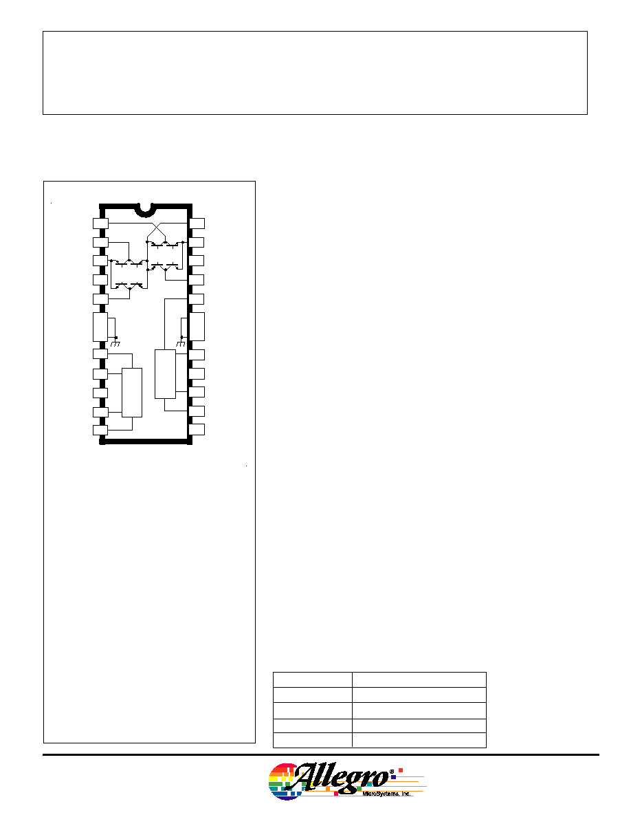
UDN2916B
(DIP)
1
2
3
4
5
6
7
8
9
24
23
22
21
20
19
18
17
16
15
14
13
12
11
10
9
2
1
V
C C
2
V
B B
1
G R OUND
G R OUND
G R OUND
G R OUND
02
I
12
I
P HAS E
2
V
R E F 2
2
R C
1
R C
V
R E F 1
P HAS E
1
11
I
2B
OUT
S E NS E
2
2
E
2A
OUT
1A
OUT
1
E
S E NS E
1
1B
OUT
01
I
LOAD
S UP P LY
LOG IC
S UP P LY
Dwg. P P -005
PW
M
1
PW
M
2
Data Sheet
29319.20F
ABSOLUTE MAXIMUM RATINGS
at T
J
150�C
Motor Supply Voltage, V
BB
.................... 45 V
Output Current, I
OUT
(Peak) ........................................ +1.0 A
(Continuous) .......................... +750 mA
Logic Supply Voltage, V
CC
................... 7.0 V
Logic Input Voltage Range,
V
IN
......................... -0.3 V to V
CC
+0.3 V
Output Emitter Voltage, V
E
.................. 1.5 V
Package Power Dissipation,
P
D
........................................................
See Graph
Operating Temperature Range,
T
A
................................. -20�C to +85�C
Storage Temperature Range,
T
S
............................... -55�C to +150�C
Output current rating may be limited by duty
cycle, ambient temperature, and heat sinking.
Under any set of conditions, do not exceed the
specified peak current rating or a junction
temperature of +150�C.
2916
115 Northeast Cutoff, Box 15036
Worcester, Massachusetts 01615-0036 (508) 853-5000
2916
DUAL FULL-BRIDGE
MOTOR DRIVER
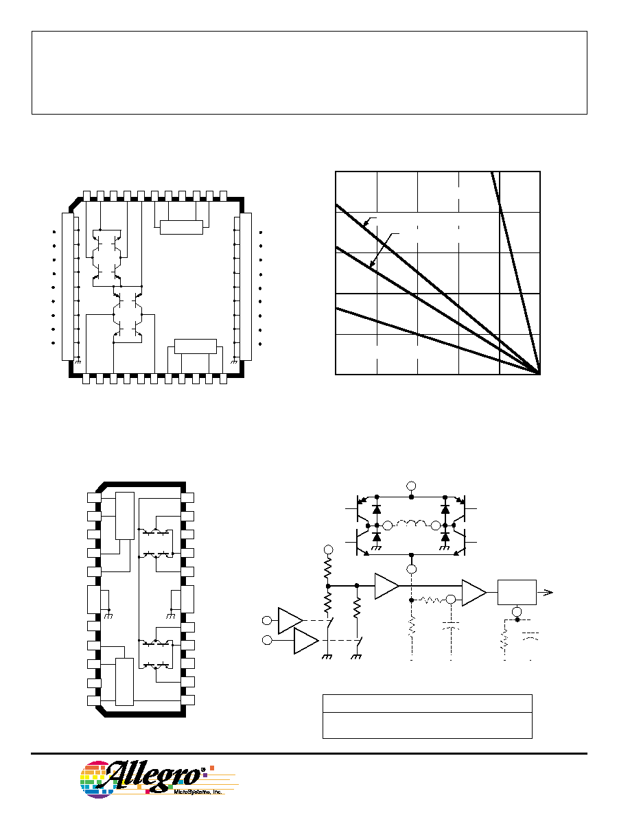
2
V
REF 2
GND
GND
GND
GND
6
5
4
3
2
1
44
43
42
41
40
7
8
9
10
11
12
13
14
15
16
17
29
30
39
38
37
36
35
34
33
32
31
28
27
26
25
24
23
22
21
20
19
18
Dwg. PP-006A
1
2
PWM 1
PWM 2
LOGIC SUPPLY
OUT
1A
E
1
SENSE
1
I
01
V
REF 1
PHASE
1
1
RC
1
I
11
OUT
1B
LOAD SUPPLY
E
2
OUT
2A
I
02
SENSE
2
PHASE
2
2
RC
2
I
12
OUT
2B
V
CC
V
BB
NO CONNECTION
NO CONNECTION
NC
NC
V
REF
Dwg. EP-007B
V
BB
SENSE
ONE
SHOT
SOURCE
DISABLE
RC
�
+
I
0
I
1
�
10
E
OUT A
OUTB
'B' PACKAGE,
CHANNEL 1
PIN NUMBERS
SHOWN.
RC
R
S
R
T
C
C
C
T
24
20 k
40 k
10 k
21
1
23
22
14
20
17
15
UDN2916EB
(PLCC)
V
BB
24
23
22
21
20
19
18
17
16
15
14
13
GROUND
GROUND
2B
OUT
SENSE
2
2
E
2A
OUT
1A
OUT
1
E
SENSE
1
1B
OUT
01
I
LOAD SUPPLY
Dwg. PP-047
1
2
3
4
5
6
7
8
9
12
11
10
9
GROUND
GROUND
02
I
12
I
PHASE
2
V
REF 2
2
RC
V
CC
1
RC
V
REF 1
PHASE
1
11
I
LOGIC SUPPLY
PWM 2
PWM 1
1
2
2
1
UDN2916LB
(SOIC)
PWM CURRENT-CONTROL CIRCUITRY
50
75
100
125
150
5
1
0
ALLOWABLE PACKAGE POWER DISSIPATION IN WATTS
TEMPERATURE IN
�
�
�
�
C
4
3
2
25
Dwg. GP-035B
R = 6.0
�
C/W
SUFFIX 'B', R = 40
�
C/W
SUFFIX 'LB', R = 77
�
C/W
SUFFIX 'EB', R = 30
�
C/W
JT
JA
JA
JA
TRUTH TABLE
PHASE
OUT
A
OUT
B
H
H
L
L
L
H
Copyright � 1994, 2003 Allegro MicroSystems, Inc.

2916
DUAL FULL-BRIDGE
MOTOR DRIVER
www.allegromicro.com
3
Limits
Characteristic
Symbol
Test Conditions
Min.
Typ.
Max.
Units
Output Drivers (OUT
A
or OUT
B
)
Motor Supply Range
V
BB
10
--
45
V
Output Leakage Current
I
CEX
V
OUT
= V
BB
--
< 1.0
50
�A
V
OUT
= 0
--
<�1.0
�50
�A
Output Sustaining Voltage
V
CE(sus)
I
OUT
= �750 mA, L = 3.0 mH
45
--
--
V
Output Saturation Voltage
V
CE(SAT)
Sink Driver, I
OUT
= +500 mA
--
0.4
0.6
V
Sink Driver, I
OUT
= +750 mA
--
1.0
1.2
V
Source Driver, I
OUT
= �500 mA
--
1.0
1.2
V
Source Driver, I
OUT
= �750 mA
--
1.3
1.5
V
Clamp Diode Leakage Current
I
R
V
R
=
45 V
--
< 1.0
50
�A
Clamp Diode Forward Voltage
V
F
I
F
= 750 mA
--
1.6
2.0
V
Driver Supply Current
I
BB(ON)
Both Bridges ON, No Load
--
20
25
mA
I
BB(OFF)
Both Bridges OFF
--
5.0
10
mA
Control Logic
Input Voltage
V
IN(1)
All inputs
2.4
--
--
V
V
IN(0)
All inputs
--
--
0.8
V
Input Current
I
IN(1)
V
IN
= 2.4 V
--
<1.0
20
�A
V
IN
= 0.8 V
--
� 3.0
�200
�A
Reference Voltage Range
V
REF
Operating
1.5
--
7.5
V
Current Limit Threshold
V
REF
/ V
SENSE
I
0
= I
1
= 0.8 V
9.5
10
10.5
--
I
0
= 2.4 V, I
1
= 0.8 V
13.5
15
16.5
--
I
0
= 0.8 V, I
1
= 2.4 V
25.5
30
34.5
--
Thermal Shutdown Temperature
T
J
--
170
--
�C
Total Logic Supply Current
I
CC(ON)
I
0
= I
1
= 0.8 V, No Load
--
40
50
mA
I
CC(OFF)
I
0
= I
1
= 2.4 V, No Load
--
10
12
mA
Fixed Off-Time
t
off
R
T
= 56 k
, C
T
= 820 pF
--
46
--
�s
ELECTRICAL CHARACTERISTICS at T
A
= +25�C, T
J
150�C, V
BB
= 45 V, V
CC
= 4.75 V to 5.25 V,
V
REF
= 5.0 V (unless otherwise noted).
(at trip point)
115 Northeast Cutoff, Box 15036
Worcester, Massachusetts 01615-0036 (508) 853-5000
2916
DUAL FULL-BRIDGE
MOTOR DRIVER
4
APPLICATIONS INFORMATION
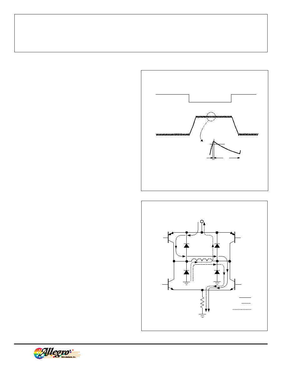
PWM CURRENT CONTROL
The UDN2916B/EB/LB dual bridges are designed to
drive both windings of a bipolar stepper motor. Output
current is sensed and controlled independently in each
bridge by an external sense resistor (R
S
), internal com-
parator, and monostable multivibrator.
When the bridge is turned ON, current increases in
the motor winding and it is sensed by the external sense
resistor until the sense voltage (V
SENSE
) reaches the level
set at the comparator's input:
I
TRIP
= V
REF
/10 R
S
The comparator then triggers the monostable which
turns OFF the source driver of the bridge. The actual
load current peak will be slightly higher than the trip point
(especially for low-inductance loads) because of the
internal logic and switching delays. This delay (t
d
) is
typically 2 �s. After turn-off, the motor current decays,
circulating through the ground-clamp diode and sink
transistor. The source driver's OFF time (and therefore
the magnitude of the current decrease) is determined by
the monostable's external RC timing components, where
t
off
= R
T
C
T
within the range of 20 k
to 100 k
and
100 pF to 1000 pF.
The fixed-off time should be short enough to keep
the current chopping above the audible range (< 46 �s)
and long enough to properly regulate the current. Be-
cause only slow-decay current control is available, short
off times (< 10 �s) require additional efforts to ensure
proper current regulation. Factors that can negatively
affect the ability to properly regulate the current when
using short off times include: higher motor-supply volt-
age, light load, and longer than necessary blank time.
When the source driver is re-enabled, the winding
current (the sense voltage) is again allowed to rise to the
comparator's threshold. This cycle repeats itself, main-
taining the average motor winding current at the desired
level.
Loads with high distributed capaci-tances may
result in high turn-ON current peaks. This peak (appear-
ing across R
S
) will attempt to trip the comparator, result-
ing in erroneous current control or high-frequency
oscillations. An external R
C
C
C
time delay should be used
to further delay the action of the comparator. Depending
on load type, many applications will not require these
external components (SENSE connected to E).
PWM OUTPUT CURRENT WAVE FORM
LOAD CURRENT PATHS
+
�
0
Dwg. W M-003-1A
V
P HAS E
I
OUT
t
d
t
off
I
T R IP
Dwg. E P -006-1
R S
B B
V
B R IDG E ON
S OUR C E OF F
ALL OF F

2916
DUAL FULL-BRIDGE
MOTOR DRIVER
www.allegromicro.com
5
LOGIC CONTROL OF OUTPUT CURRENT
Two logic level inputs (l
0
and I
1
) allow digital selection of the motor
winding current at 100%, 67%, 33%, or 0% of the maximum level per
the table. The 0% output current condition turns OFF all drivers in the
bridge and can be used as an OUTPUT ENABLE function.
CURRENT-CONTROL TRUTH TABLE
l
0
I
1
Output Current
L
L
V
REF
/10 R
S
= I
TRIP
H
L
V
REF
/15 R
S
= 2/3 I
TRIP
L
H
V
REF
/30 R
S
= 1/3 I
TRIP
H
H
0
These logic level inputs greatly enhance the implementation of
�P-controlled drive formats.
During half-step operations, the l
0
and l
1
allow the �P to control the
motor at a constant torque between all positions in an eight-step
TYPICAL APPLICATION
sequence. This is accomplished by digitally
selecting 100% drive current when only one
phase is ON and 67% drive current when two
phases are ON. Logic highs on both l
0
and l
1
turn OFF all drivers to allow rapid current
decay when switching phases. This helps to
ensure proper motor operation at high step
rates.
The logic control inputs can also be
used to select a reduced current level (and
reduced power dissipation) for `hold' condi-
tions and/or increased current (and available
torque) for start-up conditions.
GENERAL
The PHASE input to each bridge
determines the direction motor winding
current flows. An internally generated
deadtime (approximately 2 �s) prevents
crossover currents that can occur when
switching the PHASE input.
All four drivers in the bridge output can
be turned OFF between steps (l
0
= l
1
z 2.4 V)
resulting in a fast current decay through the
internal output clamp and flyback diodes. The
fast current decay is desirable in half-step and
high-speed applications. The PHASE, l
0
,and I
1
inputs float high.
Varying the reference voltage (V
REF
)
provides continuous control of the peak load
current for micro-stepping applications.
Thermal protection circuitry turns OFF
all drivers when the junction temperature
reaches +170�C. It is only intended to protect
the device from failures due to excessive
junction temperature and should not imply
that output short circuits are permitted. The
output drivers are re-enabled when the
junction temperature cools to +145�C.
The UDN2916B/EB/LB output drivers
are optimized for low output saturation
voltages--less than 1.8 V total (source plus
sink) at 500 mA. Under normal operating
conditions, when combined with the excellent
thermal properties of the batwing package
design, this allows continuous operation of
both bridges simultaneously at 500 mA.
FROM
�P
V
REF
Dwg. EP-008B1
V
BB
FROM
�P
1
2
3
4
5
6
7
8
9
24
23
22
21
20
19
18
17
16
15
14
13
12
11
10
9
2
V
CC
2
V
BB
1
V
REF
+5 V
STEPPER
MOTOR
R
S
R
S
R
C
R
C
R
T
C
T
C
C
C
C
+
PWM 1
PWM 2
1
820 pF
56 k
C
T
820 pF
56 k
R
T