 | –≠–ª–µ–∫—Ç—Ä–æ–Ω–Ω—ã–π –∫–æ–º–ø–æ–Ω–µ–Ω—Ç: UGN3175UA | –°–∫–∞—á–∞—Ç—å:  PDF PDF  ZIP ZIP |

These Hall-effect latches are temperature-stable and stress-resistant
sensors especially suited for electronic commutation in brushless dc
motors using multipole ring magnets. Each device includes a voltage
regulator, quadratic Hall voltage generator, temperature compensation
circuit, signal amplifier, Schmitt trigger, and an open-collector output on
a single silicon chip. The on-board regulator permits operation with
supply voltages of 4.5 volts to 18 volts. The switch output can sink
10 mA. With suitable output pull up, they can be used directly with
bipolar or MOS logic circuits.
The three package styles available provide a magnetically optimized
package for most applications. Suffix `LT' is a surface-mount SOT-89/
TO-243AA package; suffixes `U' and `UA' feature wire leads for
through-hole mounting.
HALL-EFFECT LATCHES
Always order by complete part number, e.g.,
UGN3175LT .
See Magnetic Characteristics table for differences between devices.
Data
Sheet
27609.4A
FEATURES
I Symmetrical Response
I 4.5 V to 18 V Operation
I Open-Collector Output
I Reverse Battery Protection
I Activate With Small, Commercially Available Permanent Magnets
I Solid-State Reliability
I Small Size
I Superior Temperature Stability
I Resistant to Physical Stress
ABSOLUTE MAXIMUM RATINGS
Supply Voltage, V
CC
. . . . . . . . . . . . . 18 V
Reverse Battery Voltage, V
RCC
. . . . -18 V
Magnetic Flux Density, B . . . . Unlimited
Output OFF Voltage, V
OUT
. . . . . . . . 18 V
Continuous Output Current, I
OUT
. 15 mA
Operating Temperature Range,
T
A
. . . . . . . . . . . . . . . -20
∞
C to +85
∞
C
Storage Temperature Range,
T
S
. . . . . . . . . . . . . . . -65
∞
C to +150
∞
C
Pinning is shown viewed from branded side.
3175
AND
3177
Dwg. PH-003A
1
SUPPLY
V
CC
GROUND
3
2
OUTPUT
X

3175
AND
3177
HALL-EFFECT
LATCHES
115 Northeast Cutoff, Box 15036
Worcester, Massachusetts 01615-0036 (508) 853-5000
FUNCTIONAL BLOCK DIAGRAM
NOTE: As used here, negative flux densities are defined as less than zero (algebraic convention).
Complete part number includes a suffix denoting package type (LT, U, or UA).
T
A
= +25
∞
C
T
A
= -20
∞
C to +85
∞
C
Characteristic
Min.
Typ.
Max.
Min.
Typ.
Max.
Operate Point, B
OP
UGN3175
25
--
170
15
--
180
UGN3177
50
--
150
25
--
150
Release Point, B
RP
UGN3175
-170
--
-25
-180
--
-15
UGN3177
-150
--
-50
-150
--
-25
Hysteresis, B
hys
UGN3175
100
200
--
80
180
--
UGN3177
100
200
--
50
180
--
V
CC
X
REG.
Dwg. FH-005-2
GROUND
OUTPUT
3
2
1
Part
Number*
Limits
Characteristic
Symbol
Test Conditions
Min.
Typ.
Max.
Units
Supply Voltage
V
CC
Operating
4.5
--
18
V
Output Saturation Voltage
V
OUT(SAT)
V
CC
= 18 V, I
OUT
= 10 mA, B > B
OP
--
200
300
mV
Output Leakage Current
I
OFF
V
OUT
= 18 V, B < B
RP
--
0.05
5.0
µA
Supply Current
I
CC
V
CC
= 4.5 V, B < B
RP
(Output OFF)
--
5.0
10
mA
Output Rise Time
t
r
V
CC
= 12 V, R
L
= 1.1 k
, C
L
= 20 pF
--
0.04
2.0
µs
Output Fall Time
t
f
V
CC
= 12 V, R
L
= 1.1 k
, C
L
= 20 pF
--
0.18
2.0
µs
ELECTRICAL CHARACTERISTICS at T
A
= +25
∞
C, V
CC
= 4.5 V to 18 V (unless otherwise noted).
MAGNETIC CHARACTERISTICS in gauss; V
CC
= 4.5 V to 18 V.
Copyright © 1991, 1999, Allegro MicroSystems, Inc.

3175
AND
3177
HALL-EFFECT
LATCHES
TYPICAL OPERATING CHARACTERISTICS
Suffix "UA"
-10
10
30
50
90
AMBIENT TEMPERATURE IN
∞C
-30
Dwg. GH-020
SWITCH POINT IN GAUSS
0
100
200
-100
-200
70
V = 14 V
CC
OPERATE POINT
RELEASE POINT
1
3
2
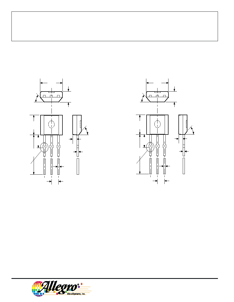
Dwg. MH-011B
0.018"
0.46 mm
NOM
BRANDED
SURFACE
ACTIVE AREA DEPTH
0.083"
2.12 mm
0.055"
1.39 mm
A
1
3
2
Dwg. MH-002-3B
0.015"
0.38 mm
NOM
BRANDED
SURFACE
ACTIVE AREA DEPTH
0.072"
1.83 mm
0.092"
2.35 mm
A
Suffix "U"
Suffix "LT"
0.045"
1.15 mm
1
3
2
Dwg. MH-008-1B
0.030"
0.76 mm
NOM
ACTIVE AREA DEPTH
0.090"
2.30 mm
A
SENSOR LOCATIONS
(
±0.005" [0.13mm] die placement)
3175
AND
3177
HALL-EFFECT
LATCHES
115 Northeast Cutoff, Box 15036
Worcester, Massachusetts 01615-0036 (508) 853-5000
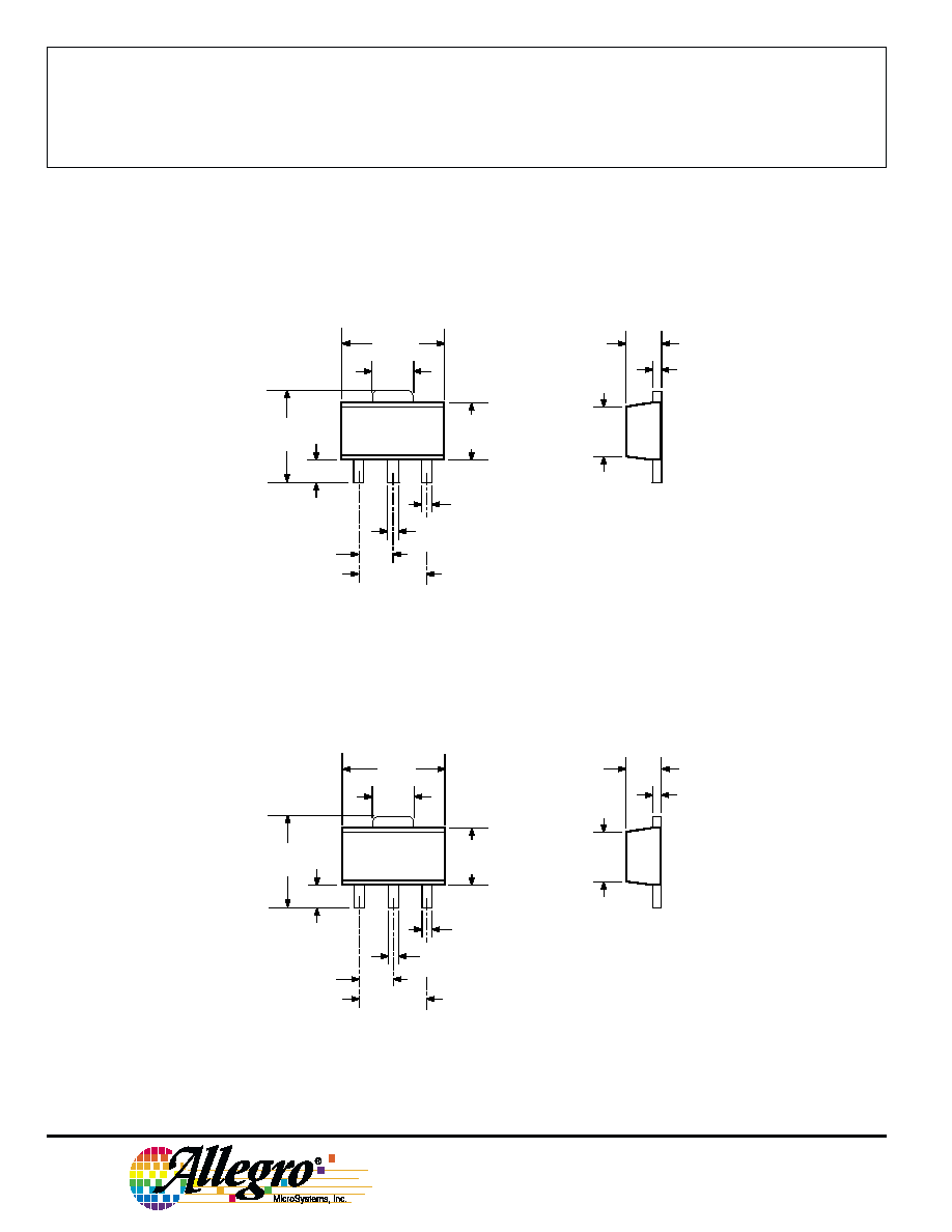
PACKAGE DESIGNATOR `LT'
Dimensions in Inches
(for reference only)
Dimensions in Millimeters
(controlling dimensions)
Dwg. MA-009-3 in
1
2
3
0.064
0.072
0.155
0.167
0.059
BSC
0.014
0.019
0.035
0.047
0.090
0.102
0.055
0.063
0.014
0.017
0.084
0.090
0.017
0.022
0.118
BSC
0.173
0.181
Dwg. MA-009-3 mm
1
2
3
4.40
4.60
1.62
1.83
3.94
4.25
1.50
BSC
0.36
0.48
0.89
1.20
2.29
2.60
1.40
1.60
0.35
0.44
2.13
2.29
0.44
0.56
3.00
BSC

3175
AND
3177
HALL-EFFECT
LATCHES
NOTES: 1. Tolerances on package height and width represent allowable mold offsets. Dimensions given are
measured at the widest point (parting line).
2. Exact body and lead configuration at vendor's option within limits shown.
3. Height does not include mold gate flash.
4. Recommended minimum PWB hole diameter to clear transition area is 0.035" (0.89 mm).
PACKAGE DESIGNATOR `U'
Dimensions in Inches
Dimensions in Millimeters
(controlling dimensions)
(for reference only)
Dwg. MH-003D in
0.063
0.059
0.018
0.015
0.016
0.050
1
2
3
0.100
45
∞
SEE NOTE
0.183
0.178
0.181
0.176
0.600
0.560
0.086
MAX
Dwg. MH-003D mm
1.60
1.50
0.46
0.38
0.41
1.27
1
2
3
2.54
45
∞
SEE NOTE
4.65
4.52
4.60
4.47
15.24
14.23
2.18
MAX
Devices in the `U' package are
NOT RECOMMENDED FOR NEW DESIGN
3175
AND
3177
HALL-EFFECT
LATCHES
115 Northeast Cutoff, Box 15036
Worcester, Massachusetts 01615-0036 (508) 853-5000
PACKAGE DESIGNATOR `UA'
Dimensions in Inches
Dimensions in Millimeters
(controlling dimensions)
(for reference only)
NOTES: 1. Tolerances on package height and width represent allowable mold offsets. Dimensions given are measured at the widest point
(parting line).
2. Exact body and lead configuration at vendor's option within limits shown.
3. Height does not include mold gate flash.
Dwg. MH-014D in
0.164
0.159
0.062
0.058
0.015
0.050
BSC
45
∞
0.640
0.600
0.016
0.085
MAX
45
∞
0.031
1
2
3
0.122
0.117
SEE NOTE
Dwg. MH-014D mm
4.17
4.04
1.57
1.47
0.38
1.27
BSC
45
∞
16.26
15.24
0.41
2.16
MAX
45
∞
0.79
1
2
3
3.10
2.97
SEE NOTE

3175
AND
3177
HALL-EFFECT
LATCHES
HALL-EFFECT SENSORS SELECTION GUIDE
Partial Part
Avail. Oper.
Characteristics at TA = +25
∞
C
Number
Temp.
BOP(max)
BRP(min)
Bhys(typ)
Features
Notes
HALL-EFFECT UNIPOLAR SWITCHES in order of BOP and Bhys
3240
E/L
+50
+5.0
10
chopper stabilized
1
3210
E
±70
±5.0
7.7
micropower, chopper stabilized
3361
E
+120
+50
5.0*
2-wire, chopper stabilized
3362
E
+120
+50
5.0*
2-wire, chopper stabilized
3161
E
+160
+30
20
2-wire
3141
E/L
+160
+10
55
3235
S
+175
+25
15*
output 1
2
-25
-175
15*
output 2
2
5140
E
+200
+50
55
300 mA output
1, 3
3142
E/L
+230
+75
55
3143
E/L
+340
+165
55
3144
E/L
+350
+50
55
3122
E/L
+400
+140
105
3123
E/L
+440
+180
105
3121
E/L
+450
+125
105
3150
J
+40 to +850
≠
20
programmable, chopper stabilized
1
HALL-EFFECT LATCHES & BIPOLAR SWITCHES
in order of BOP and Bhys
3260
E/L
+30
-30
20
bipolar, chopper stabilized
3280
E/L
+40
-40
45
chopper stabilized
3134
E/L
+50
-50
27
bipolar switch
3133
K/L/S
+75
-75
52
bipolar switch
3281
E/L
+90
-90
100
chopper stabilized
3132
K/L/S
+95
-95
52
bipolar switch
3187
E/L
+150
-150
100*
3177
S
+150
-150
200
3625
S
+150
-150
200
900 mA outputs
1, 3, 5
3626
S
+150
-150
200
400 mA outputs
1, 3, 5
3195
E/L
+160
-160
220
1, 4
3197
L
+160
-160
230
1
3175
S
+170
-170
200
3188
E/L
+180
-180
200*
3283
E/L
+180
-180
300
chopper stabilized
3189
E/L
+230
-230
100*
3275
S
+250
-250
100*
5
3185
E/L
+270
-270
340*
Operating Temperature Ranges:
S = -20
∞C to +85∞C, E = -40∞C to +85∞C, J = -40∞C to +115∞C, K = -40∞C to +125∞C, L = -40∞C to +150∞C
Notes 1. Protected.
2. Output 1 switches on south pole, output 2 switches on north pole for 2-phase, bifilar-wound, unipolar-driven brushless dc
motor control.
3. Power driver output.
4. Active pull down.
5. Complementary outputs for 2-phase bifilar-wound, unipolar-driven brushless dc motor control.
* Minimum.
Latches will not switch on removal of magnetic field; bipolar switches may switch on removal of field but require field
reversal for reliable operation over operating temperature range.

3175
AND
3177
HALL-EFFECT
LATCHES
115 Northeast Cutoff, Box 15036
Worcester, Massachusetts 01615-0036 (508) 853-5000
Allegro MicroSystems, Inc. reserves the right to make, from time to
time, such departures from the detail specifications as may be
required to permit improvements in the design of its products.
The information included herein is believed to be accurate and
reliable. However, Allegro MicroSystems, Inc. assumes no responsi-
bility for its use; nor for any infringements of patents or other rights of
third parties which may result from its use.