Alpha Industries, Inc. [781] 935-5150
∑ Fax [617] 824-4579 ∑ Email sales@alphaind.com ∑ www.alphaind.com
1
Specifications subject to change without notice. 12/99A
28≠40 GHz GaAs MMIC
Low Noise Amplifier
Features
I Single Bias Supply Operation (4.5 V)
I 3.8 dB Typical Noise Figure at 38 GHz
I 17 dB Typical Small Signal Gain
I 0.25 µm Ti/Pd/Au Gates
I 100% On-Wafer RF, DC and Noise Figure
Testing
I 100% Visual Inspection to MIL-STD-883
MT 2010
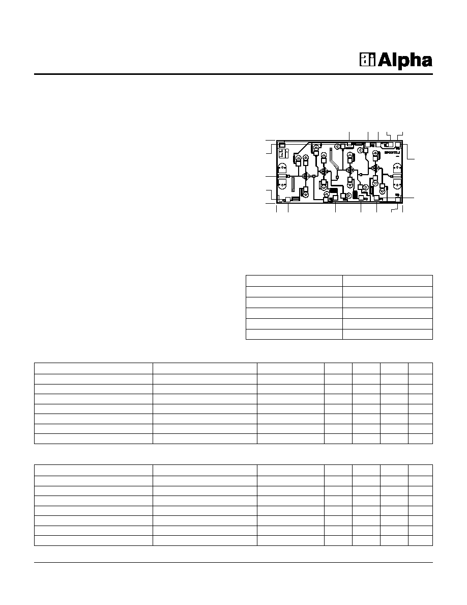
Chip Outline
AA038N1-00, AA038N2-00
Description
Alpha's four-stage reactively-matched 28≠40 GHz GaAs
MMIC low noise amplifier has typical small signal gain of
17 dB with a typical noise figure of 3.8 dB at 38 GHz. The
chip uses Alpha's proven 0.25
µm low noise PHEMT
technology, and is based upon MBE layers and electron
beam lithography for the highest uniformity and
repeatability. The FETs employ surface passivation to
ensure a rugged, reliable part with through-substrate via
holes and gold-based backside metallization to facilitate
a conductive epoxy die attach process.
Parameter
Condition
Symbol
Min.
Typ.
3
Max.
Unit
Drain Current
I
DS
35 50
mA
Small Signal Gain
F = 28≠40 GHz
G
15
17
dB
Noise Figure
F = 38 GHz
NF
3.8
4.2
dB
Input Return Loss
F = 28≠40 GHz
RL
I
-10
-6
dB
Output Return Loss
F = 28≠40 GHz
RL
O
-8
-6
dB
Output Power at 1 dB Gain Compression
1
F = 38 GHz
P
1 dB
6
dBm
Thermal Resistance
2
JC
101
∞C/W
Electrical Specifications at 25∞C (V
DS
= 4.5 V)
AA038N1-00
Parameter
Condition
Symbol
Min.
Typ.
3
Max.
Unit
Drain Current
I
DS
35
50
mA
Small Signal Gain
F = 37≠39.5 GHz
G
17
19
dB
Noise Figure
F = 38 GHz
NF
3.8
4.2
dB
Input Return Loss
F = 37≠39.5 GHz
RL
I
-14
-6
dB
Output Return Loss
F = 37≠39.5 GHz
RL
O
-11
-8
dB
Output Power at 1 dB Gain Compression
1
F = 38 GHz
P
1 dB
6
dBm
Thermal Resistance
2
JC
101
∞C/W
AA038N2-00
1. Not measured on a 100% basis.
2. Calculated value based on measurement of discrete FET.
3. Typical represents the median parameter value across the specified
frequency range for the median chip.
0.000
0.000
0.588
0.246
1.264
1.813
2.146
2.710
2.600
0.087
0.124
1.355
1.560
1.961
2.183
2.445
2.599
1.267
1.274
Dimensions indicated in mm.
All DC (V) pads are 0.1 x 0.1 mm and RF In, Out pads are 0.07 mm wide.
Chip thickness = 0.1 mm.
Characteristic
Value
Operating Temperature (T
C
)
-55∞C to +90∞C
Storage Temperature (T
ST
)
-65∞C to +150∞C
Bias Voltage (V
D
)
6 V
DC
Power In (P
IN
)
10 dBm
Junction Temperature (T
J
)
175∞C
Absolute Maximum Ratings

28≠40 GHz GaAs MMIC Low Noise Amplifier
AA038N1-00, AA038N2-00
2
Alpha Industries, Inc. [781] 935-5150
∑ Fax [617] 824-4579 ∑ Email sales@alphaind.com ∑ www.alphaind.com
Specifications subject to change without notice. 12/99A
-30
-20
-10
0
10
20
30
18 20 22 24 26 28 30 32 34 36 38 40 42
Frequency (GHz)
(dB)
Typical Small Signal Performance
S-Parameters (V
D
= 4.5 V)
S
21
S
11
S
22
Typical Gain and Noise Figure
Performance for Three Bias Conditions
Frequency (GHz)
Noise Figure (dB)
Gain (dB)
2
3
4
5
6
7
8
9
10
11
18 20 22 24 26 28 30 32 34 36 38 40 42
13
15
17
19
21
23
25
27
29
31
Gain* 3.0 V, 5.5 V
Gain 2.5 V
Gain 4.5 V
NF 4.5 V
NF 2.5 V
NF* 3.0 V, 5.5 V
Typical Gain and Noise Figure
Performance vs. Drain Bias (V
D1
= V
D2
)
V
D1
and V
D2
(V)
1.0
2.0
3.0
4.0
5.0
6.0
38 GHz Gain (dB) and
38 GHz Noise Figure (dB)
Drain Current (mA)
3
5
7
9
11
13
15
17
19
21
23
16
18
20
22
24
26
28
30
32
34
36
Gain
I
D
NF
Typical Performance Data
V
D2
RF IN
RF OUT
.01
µF 50 pF
.01
µF 50 pF
V
D1
Bias Arrangement
D
G
Detail A
RF IN
RF OUT
G
D
G
D
G
D
G
D
V
D1
V
D2
SEE
DETAIL
A
Circuit Schematic
For biasing on, adjust V
D
from zero to the desired value
(4.5 V recommended). For biasing off, reverse the biasing on procedure.
*Special Bias: V
D1
= 3.0 V, V
D2
= 5.5 V