April 2004
Copyright © Alliance Semiconductor. All rights reserved.
AS7C3256A
4/23/04; v.2.0
Alliance Semiconductor
P. 1 of 9
3.3V 32K X 8 CMOS SRAM (Common I/O)
Æ
Features
∑ Pin compatible with AS7C3256
∑ Industrial and commercial temperature options
∑ Organization: 32,768 words ◊ 8 bits
∑ High speed
- 10/12/15/20 ns address access time
- 5, 6, 7, 8 ns output enable access time
∑ Very low power consumption: ACTIVE
- 180mW max @ 10 ns
∑ Very low power consumption: STANDBY
- 7.2 mW max CMOS I/O
∑ Easy memory expansion with CE and OE inputs
∑ TTL-compatible, three-state I/O
∑ 28-pin JEDEC standard packages
- 300 mil SOJ
- 8
◊ 13.4 mm TSOP 1
∑ ESD protection
2000 volts
∑ Latch-up current
200 mA
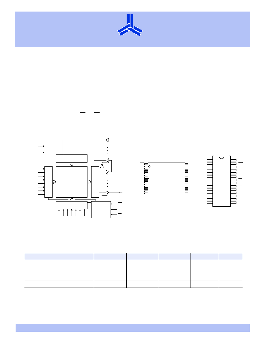
Logic block diagram
A
9
A
8
256 X 128 X 8
Array
(262,144)
Input buffer
A0
A1
A2
A3
A4
A5
A6
A7
A
10
A
11
A
12
A
13
A
14
I/O0
I/O7
V
CC
GND
OE
CE
WE
Column decoder
Row decode
r
Control
circuit
S
e
ns
e
amp
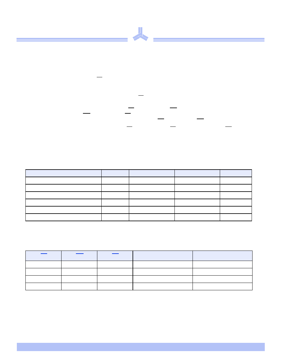
Pin arrangement
1
2
3
4
5
6
7
8
9
10
11
12
13
14
28
27
26
25
24
23
22
21
20
19
18
17
V
CC
WE
A13
A8
A9
A11
OE
A10
CE
I/O7
I/O6
I/O5
I/O4
I/O3
A14
A12
A7
A6
A5
A4
A3
A2
A1
A0
I/O0
I/O1
I/O2
GND
AS7C3256A
16
15
1
2
3
4
5
6
7
8
9
10
11
12
13
14
28
27
26
25
24
23
22
21
20
19
18
17
V
CC
WE
A13
A8
A9
A11
OE
A10
CE
I/O7
I/O6
I/O5
I/O4
I/O3
A14
A12
A7
A6
A5
A4
A3
A2
A1
A0
I/O0
I/O1
I/O2
GND
AS7C
3256A
16
15
28-pin TSOP 1 (8◊13.4 mm)
28-pin SOJ (300 mil)
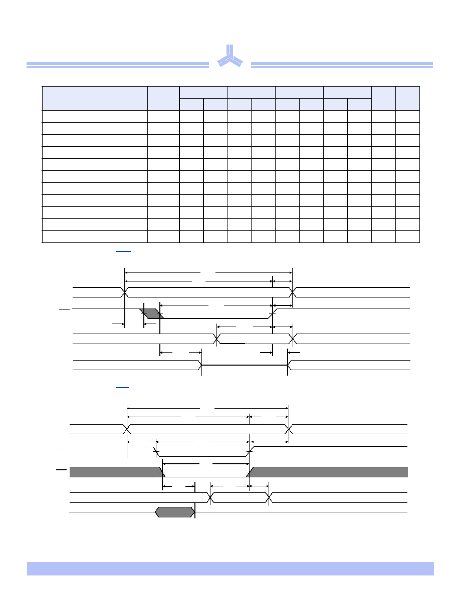
Selection guide
-10
-12
-15
-20
Unit
Maximum address access time
10
12
15
20
ns
Maximum output enable access time
5
6
7
8
ns
Maximum operating current
50
45
40
35
mA
Maximum CMOS standby current
2
2
2
2
mA
Æ
AS7C3256A
4/23/04; v.2.0
Alliance Semiconductor
P. 2 of 9
Functional description
The AS7C3256A is a 3.3V high-performance CMOS 262,144-bit Static Random-Access Memory (SRAM) device
organized as 32,768 words ◊ 8 bits. It is designed for memory applications requiring fast data access at low voltage,
including Pentium
TM
, PowerPC
TM
, and portable computing. Alliance's advanced circuit design and process techniques
permit 3.3V operation without sacrificing performance or operating margins.
The device enters standby mode when
CE
is high. CMOS standby mode consumes 7.2 mW. Normal operation offers 75%
power reduction after initial access, resulting in significant power savings during CPU idle, suspend, and stretch mode.
Equal address access and cycle times (t
AA
, t
RC
, t
WC
) of 10/12/15/20 ns with output enable access times (t
OE
) of 5, 6, 7, 8 ns
are ideal for high-performance applications. The chip enable (
CE
) input permits easy memory expansion with multiple-bank
memory organizations.
A write cycle is accomplished by asserting chip enable (CE) and write enable (WE) LOW. Data on the input pins I/O0-I/O7
is written on the rising edge of WE (write cycle 1) or CE (write cycle 2). To avoid bus contention, external devices should
drive I/O pins only after outputs have been disabled with output enable (OE) or write enable (WE).
A read cycle is accomplished by asserting chip enable (
CE
) and output enable (
OE
) LOW, with write enable (
WE
) high. The
chip drives I/O pins with the data word referenced by the input address. When chip enable or output enable is high, or write
enable is low, output drivers stay in high-impedance mode.
All chip inputs and outputs are TTL-compatible. Operation is from a single 3.3 ±0.3V supply. The AS7C3256A is packaged
in high volume industry standard packages.
Absolute maximum ratings
Stresses greater than those listed under Absolute Maximum Ratings may cause permanent damage to the device. This is a stress rating only and functional
operation of the device at these or any other conditions outside those indicated in the operational sections of this specification is not implied. Exposure to
absolute maximum rating conditions for extended periods may affect reliability.
Truth table
Key
:
X = Don't care, L = Low, H = High
Parameter
Symbol
Min
Max
Unit
Voltage on V
CC
relative to GND
V
t1
≠0.5
+5.0
V
Voltage on any pin relative to GND
V
t2
≠0.5
V
CC
+ 0.5
V
Power dissipation
P
D
≠
1.0
W
Storage temperature (plastic)
T
stg
≠65
+150
o
C
Ambient temperature with V
CC
applied
T
bias
≠55
+125
o
C
DC current into outputs (low)
I
OUT
≠
20
mA
CE
WE
OE
Data
Mode
H
X
X
High Z
Standby (I
SB
, I
SB1
)
L
H
H
High Z
Output disable (I
CC
)
L
H
L
D
OUT
Read (I
CC
)
L
L
X
D
IN
Write (I
CC
)
AS7C3256A
4/23/04; v.2.0
Alliance Semiconductor
P. 3 of 9
Æ
Recommended operating conditions
* V
IL
min = ≠1.0V for pulse width less than 5ns.
** V
IH
max = V
CC
+ 2.0V for pulse width less than 5ns.
DC operating characteristics (over the operating range)
1
Capacitance (f = 1MHz, T
a
= room temperature, V
CC
= NOMINAL)
2
Parameter
Symbol
Min
Typical
Max
Unit
Supply voltage
V
CC
3.0
3.3
3.6
V
Input voltage
V
IH
**
2.0
≠
V
CC
+0.5
V
V
IL
*
-0.5
≠
0.8
V
Ambient operating temperature
commercial
T
A
0
≠
70
o
C
industrial
T
A
≠40
≠
85
o
C
Parameter
Sym
Test conditions
-10
-12
-15
-20
Unit
Min
Max
Min
Max
Min
Max
Min
Max
Input leakage
current
|I
LI
| V
CC
= Max,
V
in
= GND to V
CC
≠
1
≠
1
≠
1
≠
1
µA
Output leakage
current
|I
LO
| V
CC
= Max,
V
OUT
= GND to V
CC
≠
1
≠
1
≠
1
≠
1
µA
Operating
power supply
current
I
CC
V
CC
= Max, CE
V
IL
f = f
Max
, I
OUT
= 0mA
≠
50
≠
45
≠
40
≠
35
mA
Standby power
supply current
I
SB
V
CC
= Max, CE
> V
IH
f = f
Max
≠
20
≠
20
≠
20
≠
20
mA
I
SB1
V
CC
= Max, CE
> V
CC
≠0.2V
V
IN
< 0.2V or
V
IN
> V
CC
≠0.2V, f = 0
≠
2.0
≠
2.0
≠
2.0
≠
2.0
mA
Output voltage
V
OL
I
OL
= 8 mA, V
CC
= Min
≠
0.4
≠
0.4
≠
0.4
≠
0.4
V
V
OH
I
OH
= ≠4 mA, V
CC
= Min
2.4
≠
2.4
≠
2.4
≠
2.4
≠
V
Parameter
Symbol
Signals
Test conditions
Max
Unit
Input capacitance
C
IN
A, CE, WE, OE
V
in
= 0V
5
pF
I/O capacitance
C
I/O
I/O
V
in
= V
out
= 0V
7
pF
Æ
AS7C3256A
4/23/04; v.2.0
Alliance Semiconductor
P. 4 of 9
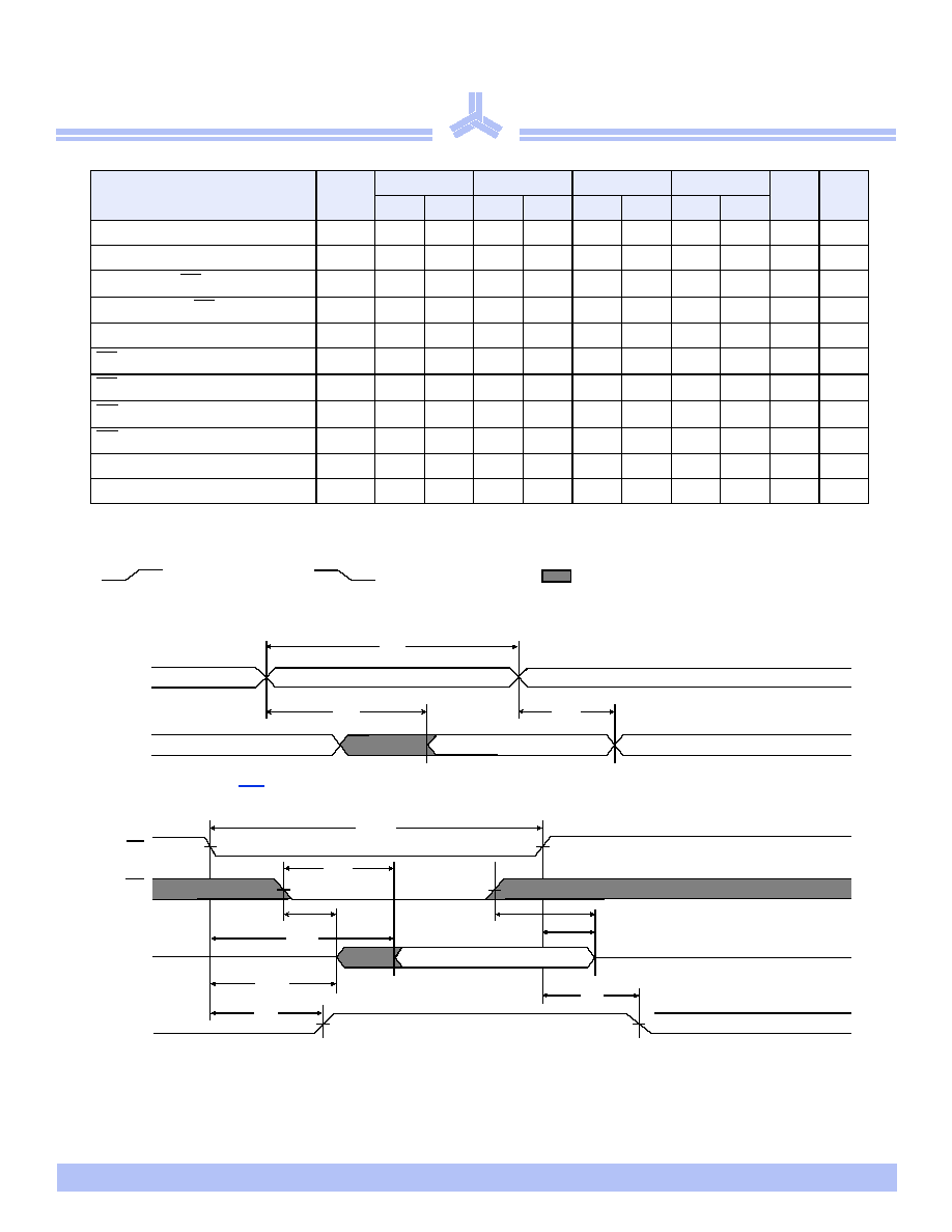
Read cycle (over the operating range)
3,9
Key to switching waveforms
Read waveform 1 (address controlled)
3,6,7,9
Read waveform 2 (CE controlled)
3,6,8,9
Parameter
Symbol
-10
-12
-15
-20
Unit Notes
Min
Max
Min
Max
Min
Max
Min
Max
Read cycle time
t
RC
10
≠
12
≠
15
≠
20
≠
ns
Address access time
t
AA
≠
10
≠
12
≠
15
≠
20
ns
3
Chip enable (CE) access time
t
ACE
≠
10
≠
12
≠
15
≠
20
ns
3
Output enable (OE) access time
t
OE
≠
5
≠
6
≠
7
≠
8
ns
Output hold from address change
t
OH
3
≠
3
≠
3
≠
3
≠
ns
5
CE LOW to output in low Z
t
CLZ
3
≠
3
≠
3
≠
3
≠
ns
4, 5
CE HIGH to output in high Z
t
CHZ
≠
3
≠
3
≠
4
≠
5
ns
4, 5
OE LOW to output in low Z
t
OLZ
0
≠
0
≠
0
≠
0
≠
ns
4, 5
OE HIGH to output in high Z
t
OHZ
≠
3
≠
3
≠
4
≠
5
ns
4, 5
Power up time
t
PU
0
≠
0
≠
0
≠
0
≠
ns
4, 5
Power down time
t
PD
≠
10
≠
12
≠
15
≠
20
ns
4, 5
Undefined output/don't care
Falling input
Rising input
Address
D
out
Data valid
t
OH
t
AA
t
RC
Supply
current
CE
OE
D
out
t
RC
1
t
OE
t
OLZ
t
ACE
t
CHZ
t
CLZ
t
PU
t
PD
I
CC
I
SB
50%
50%
t
OHZ
Data valid
AS7C3256A
4/23/04; v.2.0
Alliance Semiconductor
P. 5 of 9
Æ
Write cycle (over the operating range)
11
Write waveform 1 (WE controlled)
10,11
Write waveform 2 (CE controlled)
10,11
Parameter
Symbol
-10
-12
-15
-20
Unit Notes
Min
Max
Min
Max
Min
Max
Min
Max
Write cycle time
t
WC
10
≠
12
≠
15
≠
20
≠
ns
Chip enable to write end
t
CW
8
≠
8
≠
10
≠
12
≠
ns
Address setup to write end
t
AW
8
≠
8
≠
10
≠
12
≠
ns
Address setup time
t
AS
0
≠
0
≠
0
≠
0
≠
ns
Write pulse width
t
WP
7
≠
8
≠
9
≠
12
≠
ns
Write recovery time
t
WR
0
≠
0
≠
0
≠
0
≠
ns
Address hold from end of write
t
AH
0
≠
0
≠
0
≠
0
≠
ns
Data valid to write end
t
DW
5
≠
6
≠
8
≠
10
≠
ns
Data hold time
t
DH
0
≠
0
≠
0
≠
0
≠
ns
4, 5
Write enable to output in high Z
t
WZ
≠
5
≠
6
≠
7
≠
8
ns
4, 5
Output active from write end
t
OW
3
≠
3
≠
3
≠
3
≠
ns
4, 5
t
AW
t
AH
t
WC
Address
WE
D
in
D
out
t
DH
t
OW
t
DW
t
WZ
t
WP
t
AS
Data valid
t
WR
t
AW
Address
CE
WE
D
in
D
out
Data valid
t
CW
t
WP
t
DW
t
DH
t
AH
t
WZ
t
WC
t
AS
t
WR