Document Outline
- Features
- Logic block diagram
- Pin arrangement
- Selection guide
- Functional description
- Recommended operating conditions
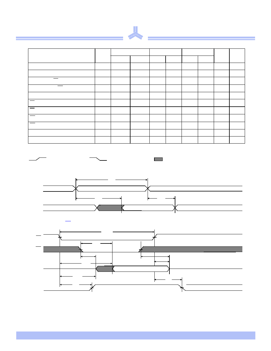
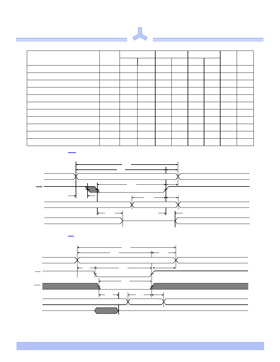
- Read cycle (over the operating range)3,9
- Key to switching waveforms
- Read waveform 1 (address controlled)3,6,7,9
- Read waveform 2 (CE controlled)3,6,8,9
- Write cycle (over the operating range)11
- Write waveform 1 (WE controlled)10,11
- Write waveform 2 (CE controlled)10,11
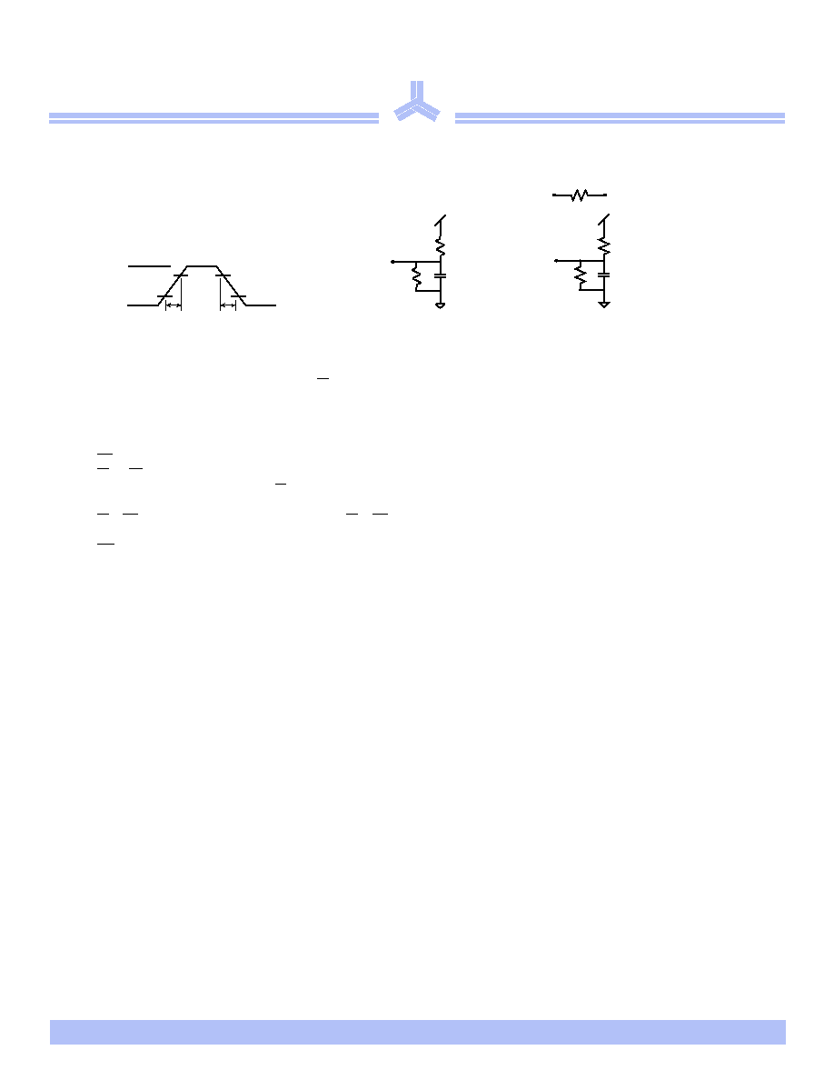
- AC test conditions
- Notes
- 1 During VCC power-up, a pull-up resistor to VCC on CE is required to meet ISB specification.
- 2 This parameter is sampled, but not 100% tested.
- 3 For test conditions, see AC Test Conditions, Figures A, B, C.
- 4 These parameters are specified with CL = 5pF, as in Figures B or C. Transition is measured ±500...
- 5 This parameter is guaranteed, but not tested.
- 6 WE is High for read cycle.
- 7 CE and OE are Low for read cycle.
- 8 Address valid prior to or coincident with CE transition Low.
- 9 All read cycle timings are referenced from the last valid address to the first transitioning ad...
- 10 CE or WE must be High during address transitions. Either CE or WE asserting high terminates a ...
- 11 All write cycle timings are referenced from the last valid address to the first transitioning ...
- 12 CE1 and CE2 have identical timing.
- 13 C=30pF, except on High Z and Low Z parameters, where C=5pF.
- Typical DC and AC characteristics
- Package diagrams
- Ordering information
September 2001
Copyright © Alliance Semiconductor. All rights reserved.
AS7C256
AS7C3256
9/18/01; v.1.6
Alliance Semiconductor
P. 1 of 9
5V/3.3V 32K X 8 CMOS SRAM (Common I/O)
Æ
Features
∑ AS7C256 (5V version)
∑ AS7C3256 (3.3V version)
∑ Industrial and commercial temperature
∑ Organization: 32,768 words ◊ 8 bits
∑ High speed
- 12/15/20 ns address access time
- 6, 7, 8 ns output enable access time
∑ Very low power consumption: ACTIVE
- 660mW (AS7C256) / max @ 12 ns
- 216mW (AS7C3256) / max @ 12 ns
∑ Very low power consumption: STANDBY
- 22 mW (AS7C256) / max CMOS I/O
- 7.2 mW (AS7C3256) / max CMOS I/O
∑ Easy memory expansion with CE and OE inputs
∑ TTL-compatible, three-state I/O
∑ 28-pin JEDEC standard packages
- 300 mil PDIP
- 300 mil SOJ
- 8
◊
13.4 mm TSOP 1
∑ ESD protection
2000 volts
∑ Latch-up current
200 mA
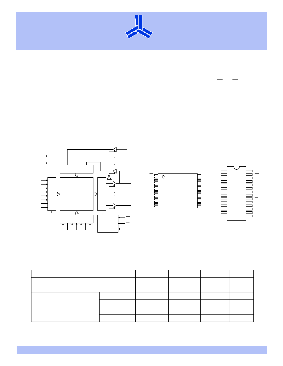
Logic block diagram
A
8
A
7
256 X 128 X 8
Array
(262,144)
Input buffer
A0
A1
A2
A3
A4
A5
A6
A14
A
9
A
10
A
11
A
12
A
13
I/O0
I/O7
V
CC
GND
OE
CE
WE
Column decoder
Ro
w d
e
c
o
d
e
r
Control
circuit
Sens
e amp
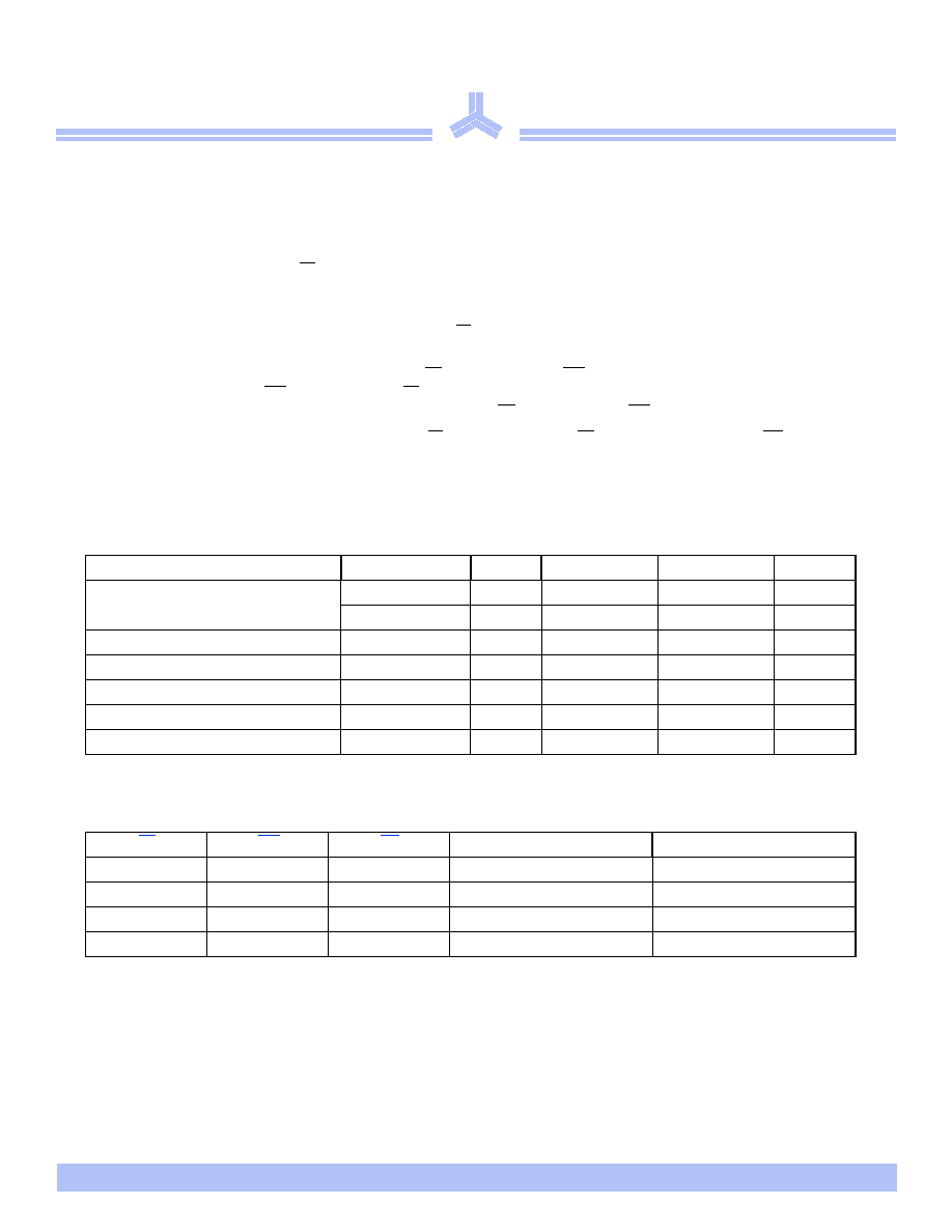
Pin arrangement
1
2
3
4
5
6
7
8
9
10
11
12
13
14
28
27
26
25
24
23
22
21
20
19
18
17
V
CC
WE
A13
$
$
A11
OE
A10
CE
I/O7
,2
I/O5
I/O4
,2
A14
A12
A7
A6
$
A4
A3
A2
A1
A0
I/O0
,2
,2
GND
A
S
7C256
A
S
7C3256
16
15
1
2
3
4
5
6
7
8
9
10
11
12
13
14
28
27
26
25
24
23
22
21
20
19
18
17
V
CC
WE
A13
A8
A9
A11
OE
A10
CE
I/O7
I/O6
I/O5
I/O4
I/O3
A14
A12
A7
A6
A5
A4
A3
A2
A1
A0
I/O0
I/O1
I/O2
GND
AS7C256
AS7C3256
16
15
28-pin TSOP 1 (8◊13.4 mm)
28-pin DIP, SOJ (300 mil)
Note: This part is compatible with both pin numbering
conventions used by various manufacturers.
(21)
(20)
(19)
(18)
(17)
(16)
(15)
(14)
(13)
(12)
(11)
(10)
(9)
(8)
(22)
(23)
(24)
(25)
(26)
(27)
(28)
(1)
(2)
(3)
(4)
(5)
(6)
(7)
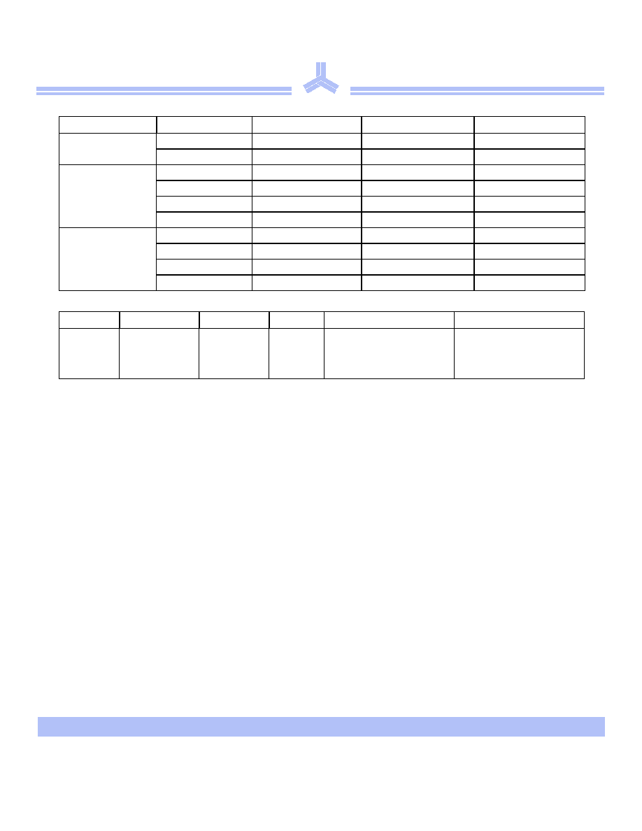
Selection guide
-12
-15
-20
Unit
Maximum address access time
12
15
20
ns
Maximum output enable access time
6
7
8
ns
Maximum operating current
AS7C256
120
115
110
mA
AS7C3256
60
55
50
mA
Maximum CMOS standby current
AS7C256
4
4
4
mA
AS7C3256
2
2
2
mA
Æ
AS7C256
AS7C3256
9/18/01; v.1.6
Alliance Semiconductor
P. 2 of 9
Functional description
The AS7C(3)256 is a 5V/3.3V high-performance CMOS 262,144-bit Static Random-Access Memory (SRAM) device organized
as 32,768 words ◊ 8 bits. It is designed for memory applications requiring fast data access at low voltage, including
Pentium
TM
, PowerPC
TM
, and portable computing. Alliance's advanced circuit design and process techniques permit 3.3V
operation without sacrificing performance or operating margins.
The device enters standby mode when
CE
is high. CMOS standby mode consumes
3.6 mW. Normal operation offers 75% power
reduction after initial access, resulting in significant power savings during CPU idle, suspend, and stretch mode.
Equal address access and cycle times (t
AA
, t
RC
, t
WC
) of 12/15/20 ns with output enable access times (t
OE
) of 6, 7, 8 ns are
ideal for high-performance applications. The chip enable (
CE
) input permits easy memory expansion with multiple-bank
memory organizations.
A write cycle is accomplished by asserting chip enable (CE) and write enable (WE) LOW. Data on the input pins I/O0-I/O7 is
written on the rising edge of WE (write cycle 1) or CE (write cycle 2). To avoid bus contention, external devices should drive
I/O pins only after outputs have been disabled with output enable (OE) or write enable (WE).
A read cycle is accomplished by asserting chip enable (
CE
) and output enable (
OE
) LOW, with write enable (
WE
) high. The
chip drives I/O pins with the data word referenced by the input address. When chip enable or output enable is high, or write
enable is low, output drivers stay in high-impedance mode.
All chip inputs and outputs are TTL-compatible and 5V tolerant. Operation is from a single 3.3±0.3V supply. The
AS7C(3)256A is packaged in high volume industry standard packages.
Absolute maximum ratings
Stresses greater than those listed under Absolute Maximum Ratings may cause permanent damage to the device. This is a stress rating only and functional operation
of the device at these or any other conditions outside those indicated in the operational sections of this specification is not implied. Exposure to absolute max-
imum rating conditions for extended periods may affect reliability.
Truth table
Key:
X = Don't care, L = Low, H = High
Parameter
Device
Symbol
Min
Max
Unit
Voltage on V
CC
relative to GND
AS7C256
V
t1
≠0.5
+7.0
V
AS7C3256
V
t1
≠0.5
+5.0
V
Voltage on any pin relative to GND
V
t2
≠0.5
V
CC
+ 0.5
V
Power dissipation
P
D
≠
1.0
W
Storage temperature (plastic)
T
stg
≠65
+150
o
C
Ambient temperature with V
CC
applied
T
bias
≠55
+125
o
C
DC current into outputs (low)
I
OUT
≠
20
mA
CE
WE
OE
Data
Mode
H
X
X
High Z
Standby (I
SB
, I
SB1
)
L
H
H
High Z
Output disable (I
CC
)
L
H
L
D
OUT
Read (I
CC
)
L
L
X
D
IN
Write (I
CC
)
AS7C256
AS7C3256
9/18/01; v.1.6
Alliance Semiconductor
P. 3 of 9
Æ
Recommended operating conditions
*
V
IL
min = ≠2.0V for pulse width less than t
RC
/2.
DC operating characteristics (over the operating range)
Capacitance (f = 1MHz, T
a
= room temperature, V
CC
= NOMINAL)
Parameter
Device
Symbol
Min
Typical
Max
Unit
Supply voltage
AS7C256
V
CC
4.5
5.0
5.5
V
AS7C3256
V
CC
3.0
3.3
3.6
V
Input voltage
AS7C256
V
IH
2.2
≠
V
CC
+0.5
V
AS7C3256
V
IH
2.0
≠
V
CC
+0.5
V
--
V
IL
*
-0.5
*
≠
0.8
V
Ambient operating temperature
commercial
T
A
0
≠
70
o
C
industrial
T
A
≠40
≠
85
o
C
Parameter
Sym Test conditions
Device
-12
-15
-20
Unit
Min
Max
Min
Max
Min
Max
Input leakage
current
|
I
LI
|
V
CC
= Max,
V
in
= GND to V
CC
Both
≠
1
≠
1
≠
1
µA
Output leakage
current
|
I
LO
|
V
CC
= Max,
V
OUT
= GND to V
CC
Both
≠
1
≠
1
≠
1
µA
Operating
power supply
current
I
CC
V
CC
= Max, CE
V
IL
f = f
Max
, I
OUT
= 0mA
AS7C256
≠
120
≠
115
≠
110
mA
AS7C3256
≠
60
≠
55
≠
50
Standby power
supply current
I
SB
V
CC
= Max, CE
V
IL
f = f
Max
, I
OUT
= 0mA
AS7C256
≠
40
≠
35
≠
30
mA
AS7C3256
≠
20
≠
20
≠
20
I
SB1
V
CC
= Max, CE
>
V
CC
≠0.2V
V
IN
< GND + 0.2V or
V
IN
> V
CC
≠0.2V, f = 0
AS7C256
≠
4.0
≠
4.0
≠
4.0
mA
AS7C3256
≠
2.0
≠
2.0
≠
2.0
Output voltage
V
OL
I
OL
= 8 mA, V
CC
= Min
Both
≠
0.4
≠
0.4
≠
0.4
V
V
OH
I
OH
= ≠4 mA, V
CC
= Min
Both
2.4
≠
2.4
≠
2.4
≠
V
Parameter
Symbol
Signals
Test conditions
Max
Unit
Input capacitance
C
IN
A, CE, WE, OE
V
in
= 0V
5
pF
I/O capacitance
C
I/O
I/O
V
in
= V
out
= 0V
7
pF
Æ
AS7C256
AS7C3256
9/18/01; v.1.6
Alliance Semiconductor
P. 4 of 9
Read cycle (over the operating range)
Key to switching waveforms
Read waveform 1 (address controlled)
Read waveform 2 (CE controlled)
Parameter
Symbol
-12
-15
-20
Unit
Notes
Min
Max
Min
Max
Min
Max
Read cycle time
t
RC
12
≠
15
≠
20
≠
ns
Address access time
t
AA
≠
12
≠
15
≠
20
ns
3
Chip enable (CE) access time
t
ACE
≠
12
≠
15
≠
20
ns
3
Output enable (OE) access time
t
OE
≠
6
≠
7
≠
8
ns
Output hold from address change
t
OH
3
≠
3
≠
3
≠
ns
5
CE LOW to output in low Z
t
CLZ
3
≠
3
≠
3
≠
ns
4, 5
CE HIGH to output in high Z
t
CHZ
≠
3
≠
4
≠
5
ns
4, 5
OE LOW to output in low Z
t
OLZ
0
≠
0
≠
0
≠
ns
4, 5
OE HIGH to output in high Z
t
OHZ
≠
3
≠
4
≠
5
ns
4, 5
Power up time
t
PU
0
≠
0
≠
0
≠
ns
4, 5
Power down time
t
PD
≠
12
≠
15
≠
20
ns
4, 5
8QGHILQHG RXWSXWGRQ∂W FDUH
)DOOLQJ LQSXW
5LVLQJ LQSXW
Address
D
RXW
Data valid
t
2+
W
$$
t
5&
Supply
current
&(
2(
D
RXW
t
5&
t
2(
t
2/=
t
$&(
t
&+=
t
&/=
t
38
t
3'
I
&&
I
6%
50%
50%
t
2+=
Data valid
AS7C256
AS7C3256
9/18/01; v.1.6
Alliance Semiconductor
P. 5 of 9
Æ
Write cycle (over the operating range)
Write waveform 1 (WE controlled)
Write waveform 2 (CE controlled)
Parameter
Symbol
-12
-15
-20
Unit
Notes
Min
Max
Min
Max
Min
Max
Write cycle time
t
WC
12
≠
15
≠
20
≠
ns
Chip enable to write end
t
CW
8
≠
10
≠
12
≠
ns
Address setup to write end
t
AW
8
≠
10
≠
12
≠
ns
Address setup time
t
AS
0
≠
0
≠
0
≠
ns
Write pulse width
t
WP
8
≠
9
≠
12
≠
ns
Write recovery time
t
WR
0
≠
0
≠
0
≠
ns
Address hold from end of write
t
AH
0
≠
0
≠
0
≠
ns
Data valid to write end
t
DW
6
≠
8
≠
10
≠
ns
Data hold time
t
DH
0
≠
0
≠
0
≠
ns
4, 5
Write enable to output in high Z
t
WZ
≠
5
≠
5
≠
5
ns
4, 5
Output active from write end
t
OW
3
≠
3
≠
3
≠
ns
4, 5
t
$:
t
$+
t
:&
Address
:(
D
LQ
D
RXW
t
'+
t
2:
t
':
t
:=
t
:3
t
$6
Data valid
t
:5
t
$:
Address
&(
:(
D
LQ
D
RXW
Data valid
t
&:
t
:3
t
':
t
'+
t
$+
t
:=
t
:&
t
$6
t
:5
Æ
AS7C256
AS7C3256
9/18/01; v.1.6
Alliance Semiconductor
P. 6 of 9
AC test conditions
Notes
1
During V
CC
power-up, a pull-up resistor to V
CC
on CE is required to meet I
SB
specification.
2
This parameter is sampled, but not 100% tested.
3
For test conditions, see AC Test Conditions, Figures A, B, C.
4
These parameters are specified with CL = 5pF, as in Figures B or C. Transition is measured
±
500mV from steady-state voltage.
5
This parameter is guaranteed, but not tested.
6
WE is High for read cycle.
7
CE and OE are Low for read cycle.
8
Address valid prior to or coincident with CE transition Low.
9
All read cycle timings are referenced from the last valid address to the first transitioning address.
10 CE or WE must be High during address transitions. Either CE or WE asserting high terminates a write cycle.
11 All write cycle timings are referenced from the last valid address to the first transitioning address.
12 CE1 and CE2 have identical timing.
13 C=30pF, except on High Z and Low Z parameters, where C=5pF.
350
C(14)
320
D
RXW
GND
+3.3V
168
D
RXW
+1.72V (5V and 3.3V)
Figure C: Output load
255
C(14)
480
D
RXW
GND
+5V
Figure B: Output lo
DG
Thevenin equivalent
- Output load: see Figure B or Figure C.
- Input pulse level: GND to 3.0V. See Figure A.
- Input rise and fall times: 2 ns. See Figure A.
- Input and output timing reference levels: 1.5V.
10%
90%
10%
90%
GND
+3.0V
Figure A: Input pulse
2 ns
AS7C256
AS7C3256
9/18/01; v.1.6
Alliance Semiconductor
P. 7 of 9
Æ
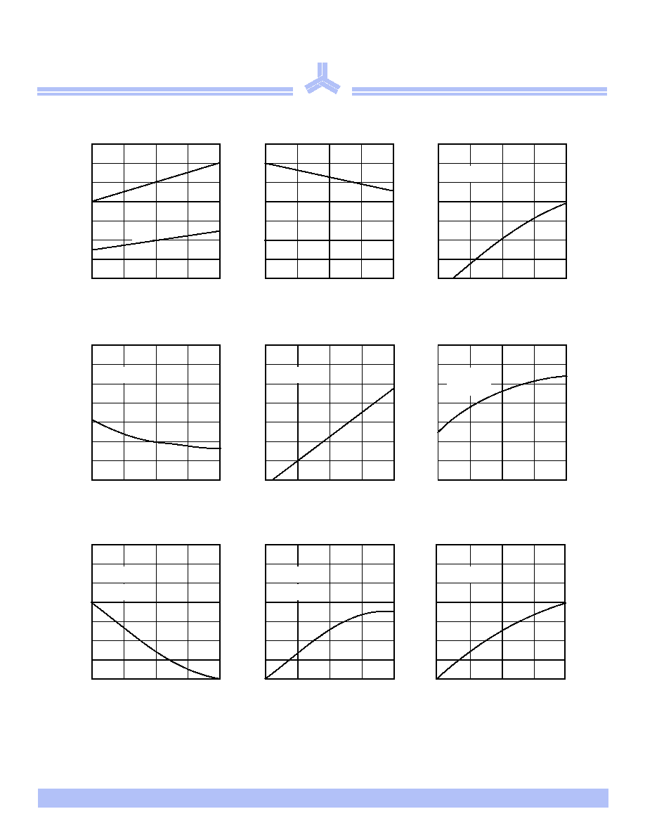
Typical DC and AC characteristics
Supply voltage (V)
MIN
MAX
NOMINAL
0.0
0.2
0.6
0.8
0.4
1.0
1.2
1.4
Nor
m
a
l
i
z
ed I
CC
, I
SB
Normalized supply current I
CC
, I
SB
Ambient temperature (∞C)
≠55
80
125
35
≠10
0.0
0.2
0.6
0.8
0.4
1.0
1.2
1.4
Nor
m
a
l
i
z
ed I
CC
, I
SB
Normalized supply current I
CC
, I
SB
vs. ambient temperature T
a
vs. supply voltage V
CC
I
CC
I
SB
I
CC
I
SB
Ambient temperature (∞C)
-55
80
125
35
-10
0.2
1
0.04
5
25
625
No
r
m
a
l
i
z
e
d
I
SB
1
(lo
g
sc
ale)
Normalized supply current ISB1
vs. ambient temperature T
a
V
CC
= V
CC
(NOMINAL)
Supply voltage (V)
MIN
MAX
NOMINAL
0.8
0.9
1.1
1.2
1.0
1.3
1.4
1.5
No
r
m
a
l
i
z
e
d
ac
ce
s
s
t
i
m
e
Normalized access time t
AA
Ambient temperature (∞C)
≠55
80
125
35
≠10
0.8
0.9
1.1
1.2
1.0
1.3
1.4
1.5
No
r
m
a
l
i
z
e
d
ac
ce
s
s
t
i
m
e
Normalized access time t
AA
Cycle frequency (MHz)
0
75
100
50
25
0.0
0.2
0.6
0.8
0.4
1.0
1.2
1.4
Nor
m
al
iz
ed I
CC
Normalized supply current I
CC
vs. ambient temperature T
a
vs. cycle frequency 1/t
RC
, 1/t
WC
vs. supply voltage V
CC
V
CC
= V
CC
(NOMINAL)
T
a
= 25∞C
V
CC
= V
CC
(NOMINAL)
T
a
= 25∞C
Output voltage (V)
V
CC
0
20
60
80
40
100
120
140
Output
source cur
r
ent (
m
A
)
Output source current I
OH
Output voltage (V)
V
CC
Output sink cur
r
ent (mA
)
Output sink current I
OL
vs. output voltage V
OL
vs. output voltage V
OH
0
20
60
80
40
100
120
140
V
CC
= V
CC
(NOMINAL)PL
T
a
= 25∞C
V
CC
= V
CC
(NOMINAL)
T
a
= 25∞C
Capacitance (pF)
0
750
1000
500
250
0
5
15
20
10
25
30
35
Cha
n
g
e
in t
AA
(ns
)
Typical access time change
t
AA
vs. output capacitive loading
V
CC
= V
CC(NOMINAL)
0
0
Æ
AS7C256
AS7C3256
9/18/01; v.1.6
Alliance Semiconductor
P. 8 of 9
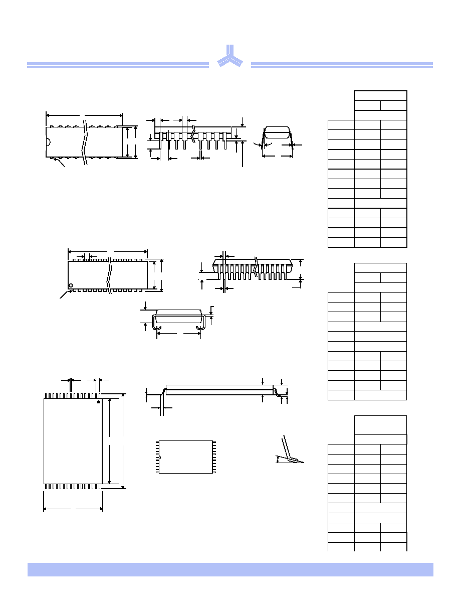
Package diagrams
c
eA
Seating
b
A1
E1 E
D
e
L
S
Plane
B
A
Pin 1
28-pin PDIP
Min
Max
in mils
A
-
0.175
A1
0.010
-
B
0.058
0.064
b
0.016
0.022
c
0.008
0.014
D
-
1.400
E
0.295
0.320
E1
0.278
0.298
e
0.100 BSC
eA
0.330
0.370
L
0.120
0.140
a
0∞
15∞
S
-
0.055
28-pin SOJ
Min
Max
in mils
A
-
0.140
A1
0.025
-
A2
0.095
0.105
B
0.028 TYP
b
0.018 TYP
c
0.010 TYP
D
-
0.730
E
0.245
0.285
E1
0.295
0.305
E2
0.327
0.347
e
0.050 BSC
28-pin
8◊13.4 mm
Min
Max
A
≠
1.20
A1
0.10
0.20
A2
0.95
1.05
b
0.15
0.25
c
0.10
0.20
D
11.60
11.80
e
0.55 nominal
E
8.0 nominal
Hd
13.30
13.50
L
0.50
0.70
0∞
5∞
H
'
(
3LQ
E
%
$
$
F
(
Seating
Plane
(
$
e
b
E
Hd
D
c
L
A1
A
A2
28-pin
pin 8(21)
pin 1(7)
pin 5(8)
pin 1(22)
Note: This part is compatible with both pin numbering
conventions used by various manufacturers.
&RS\ULJKW $OOLDQFH 6HPLFRQGXFWRU &RUSRUDWLRQ $OO ULJKWV UHVHUYHG 2XU WKUHHSRLQW ORJR RXU QDPH DQG ,QWHOOLZDWW DUH WUDGHPDUNV RU UHJLVWHUHG WUDGHPDUNV RI $OOLDQFH $OO RWKHU EUDQG DQG SURGXFW QDPHV PD\ EH WKH WUDGH
PDUNV RI WKHLU UHVSHFWLYH FRPSDQLHV $OOLDQFH UHVHUYHV WKH ULJKW WR PDNH FKDQJHV WR WKLV GRFXPHQW DQG LWV SURGXFWV DW DQ\ WLPH ZLWKRXW QRWLFH $OOLDQFH DVVXPHV QR UHVSRQVLELOLW\ IRU DQ\ HUURUV WKDW PD\ DSSHDU LQ WKLV GRFXPHQW
7KH GDWD FRQWDLQHG KHUHLQ UHSUHVHQWV $OOLDQFH∂V EHVW GDWD DQGRU HVWLPDWHV DW WKH WLPH RI LVVXDQFH $OOLDQFH UHVHUYHV WKH ULJKW WR FKDQJH RU FRUUHFW WKLV GDWD DW DQ\ WLPH ZLWKRXW QRWLFH ,I WKH SURGXFW GHVFULEHG KHUHLQ LV XQGHU
GHYHORSPHQW VLJQLILFDQW FKDQJHV WR WKHVH VSHFLILFDWLRQV DUH SRVVLEOH 7KH LQIRUPDWLRQ LQ WKLV SURGXFW GDWD VKHHW LV LQWHQGHG WR EH JHQHUDO GHVFULSWLYH LQIRUPDWLRQ IRU SRWHQWLDO FXVWRPHUV DQG XVHUV DQG LV QRW LQWHQGHG WR RSHUDWH
DV RU SURYLGH DQ\ JXDUDQWHH RU ZDUUDQWHH WR DQ\ XVHU RU FXVWRPHU $OOLDQFH GRHV QRW DVVXPH DQ\ UHVSRQVLELOLW\ RU OLDELOLW\ DULVLQJ RXW RI WKH DSSOLFDWLRQ RU XVH RI DQ\ SURGXFW GHVFULEHG KHUHLQ DQG GLVFODLPV DQ\ H[SUHVV RU
LPSOLHG ZDUUDQWLHV UHODWHG WR WKH VDOH DQGRU XVH RI $OOLDQFH SURGXFWV LQFOXGLQJ OLDELOLW\ RU ZDUUDQWLHV UHODWHG WR ILWQHVV IRU D SDUWLFXODU SXUSRVH PHUFKDQWDELOLW\ RU LQIULQJHPHQW RI DQ\ LQWHOOHFWXDO SURSHUW\ ULJKWV H[FHSW DV
H[SUHVV DJUHHG WR LQ $OOLDQFH∂V 7HUPV DQG &RQGLWLRQV RI 6DOH ZKLFK DUH DYDLODEOH IURP $OOLDQFH� $OO VDOHV RI $OOLDQFH SURGXFWV DUH PDGH H[FOXVLYHO\ DFFRUGLQJ WR $OOLDQFH∂V 7HUPV DQG &RQGLWLRQV RI 6DOH 7KH SXUFKDVH RI
SURGXFWV IURP $OOLDQFH GRHV QRW FRQYH\ D OLFHQVH XQGHU DQ\ SDWHQW ULJKWV FRS\ULJKWV PDVN ZRUNV ULJKWV WUDGHPDUNV RU DQ\ RWKHU LQWHOOHFWXDO SURSHUW\ ULJKWV RI $OOLDQFH RU WKLUG SDUWLHV $OOLDQFH GRHV QRW DXWKRUL]H LWV SURGXFWV
IRU XVH DV FULWLFDO FRPSRQHQWV LQ OLIHVXSSRUWLQJ V\VWHPV ZKHUH D PDOIXQFWLRQ RU IDLOXUH PD\ UHDVRQDEO\ EH H[SHFWHG WR UHVXOW LQ VLJQLILFDQW LQMXU\ WR WKH XVHU DQG WKH LQFOXVLRQ RI $OOLDQFH SURGXFWV LQ VXFK OLIHVXSSRUWLQJ V\V
WHPV LPSOLHV WKDW WKH PDQXIDFWXUHU DVVXPHV DOO ULVN RI VXFK XVH DQG DJUHHV WR LQGHPQLI\ $OOLDQFH DJDLQVW DOO FODLPV DULVLQJ IURP VXFK XVH
AS7C256
AS7C3256
9/18/01; v.1.6
Alliance Semiconductor
P. 9 of 9
Æ
Ordering information
Part numbering system
Package / Access time
Volt/Temp
12 ns
15 ns
20 ns
Plastic DIP, 300 mil
5V commercial
AS7C256-12PC
AS7C256-15PC
AS7C256-20PC
3.3V commercial
AS7C3256-12PC
AS7C3256-15PC
AS7C3256-20PC
Plastic SOJ, 300 mil
5V commercial
AS7C256-12JC
AS7C256-15JC
AS7C256-20JC
3.3V commercial
AS7C3256-12JC
AS7C3256-15JC
AS7C3256-20JC
5V industrial
AS7C256-12JI
AS7C256-15JI
AS7C256-20JI
3.3V industrial
AS7C3256-12JI
AS7C3256-15JI
AS7C3256-20JI
TSOP 8x13.4mm
5V commercial
AS7C256-12TC
AS7C256-15TC
AS7C256-20TC
3.3V commercial
AS7C3256-12TC
AS7C3256-15TC
AS7C3256-20TC
5V industrial
AS7C256-12TI
AS7C256-15TI
AS7C256-20TI
3.3V industrial
AS7C3256-12TI
AS7C3256-15TI
AS7C3256-20TI
AS7C
3
256
≠XX
X
C or I
SRAM prefix
Voltage:
3 = 3.3V supply
5 = 5V supply
Device number
Access time
Packages:
P = PDIP 300 mil
J = SOJ 300 mil
T = TSOP 8x13.4mm
Temperature range:
C = 0
o
C to 70
0
C
I = -40C to 85C