February 2005
Copyright © Alliance Semiconductor. All rights reserved.
AS7C33128FT32B
3.3V 128K
◊ 32/36 Flow Through Synchronous SRAM
Æ
2/8/05; v.1.2
Alliance Semiconductor
P. 1 of 19
AS7C33128FT36B
Features
∑ Organization: 131,072 words ◊ 32 or 36 bits
∑ Fast clock to data access: 6.5/7.5/8.0/10.0 ns
∑ Fast OE access time: 3.5/4.0 ns
∑ Fully synchronous flow through operation
∑ Asynchronous output enable control
∑ Available in 100-pin TQFP package
∑ Individual byte write and Global write
∑ Multiple chip enables for easy expansion
∑ 3.3V core power supply
∑ 2.5V or 3.3V I/O operation with separate V
DDQ
∑ Linear or interleaved burst control
∑ Snooze mode for reduced power standby
∑ Common data inputs and data outputs
Selection guide
≠65
-75
-80
-10
Units
Minimum cycle time
7.5
8.5
10
12
ns
Maximum clock access time
6.5
7.5
8.0
10.0
ns
Maximum operating current
275
250
215
185
mA
Maximum standby current
90
85
75
75
mA
Maximum CMOS standby current (DC)
30
30
30
30
mA
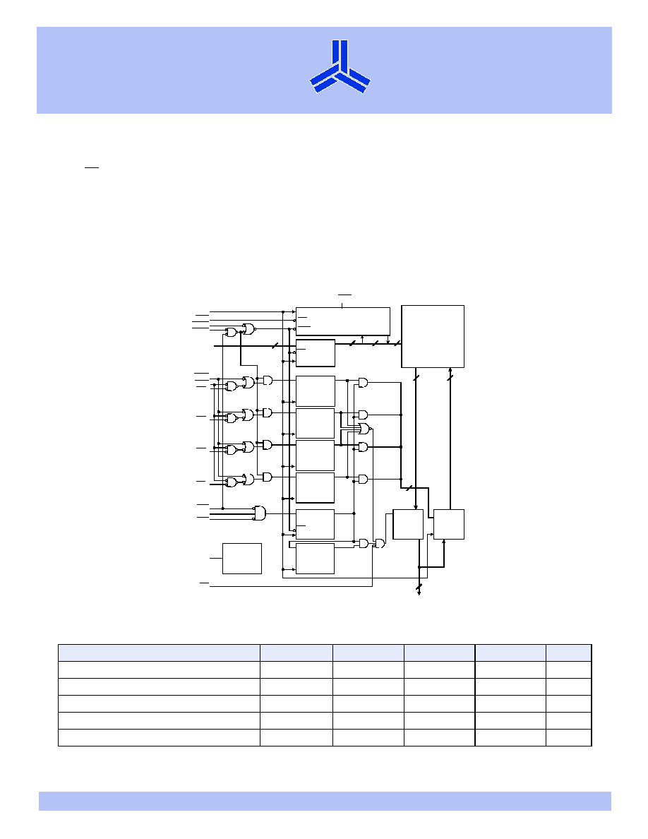
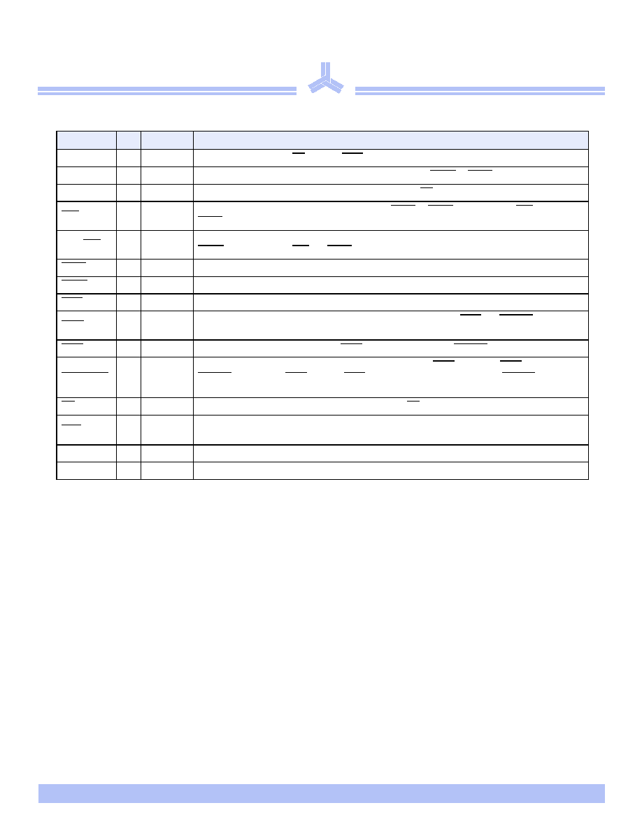
Logic block diagram
Q0
Q1
128K ◊ 32/36
Memory
array
Burst logic
CLK
CLR
CE
Address
D
Q
CE
CLK
DQ
d
CLK
D
Q
Byte write
registers
register
DQ
c
CLK
D
Q
Byte write
registers
DQ
b
CLK
D
Q
Byte write
registers
DQ
a
CLK
D
Q
Byte write
registers
Enable
CLK
D
Q
register
Enable
CLK
D
Q
delay
register
CE
Output
buffer
Input
registers
Power
down
DQ[a:d]
4
36/32
19
17
19
19
GWE
BWE
BW
d
ADV
ADSC
ADSP
CLK
CE0
CE1
CE2
BW
c
BW
b
BW
a
OE
ZZ
LBO
OE
CLK
36/32
36/32
A[18:0]
AS7C33128FT32B
Æ
2/8/05; v.1.2
Alliance Semiconductor
P. 2 of 19
AS7C33128FT36B
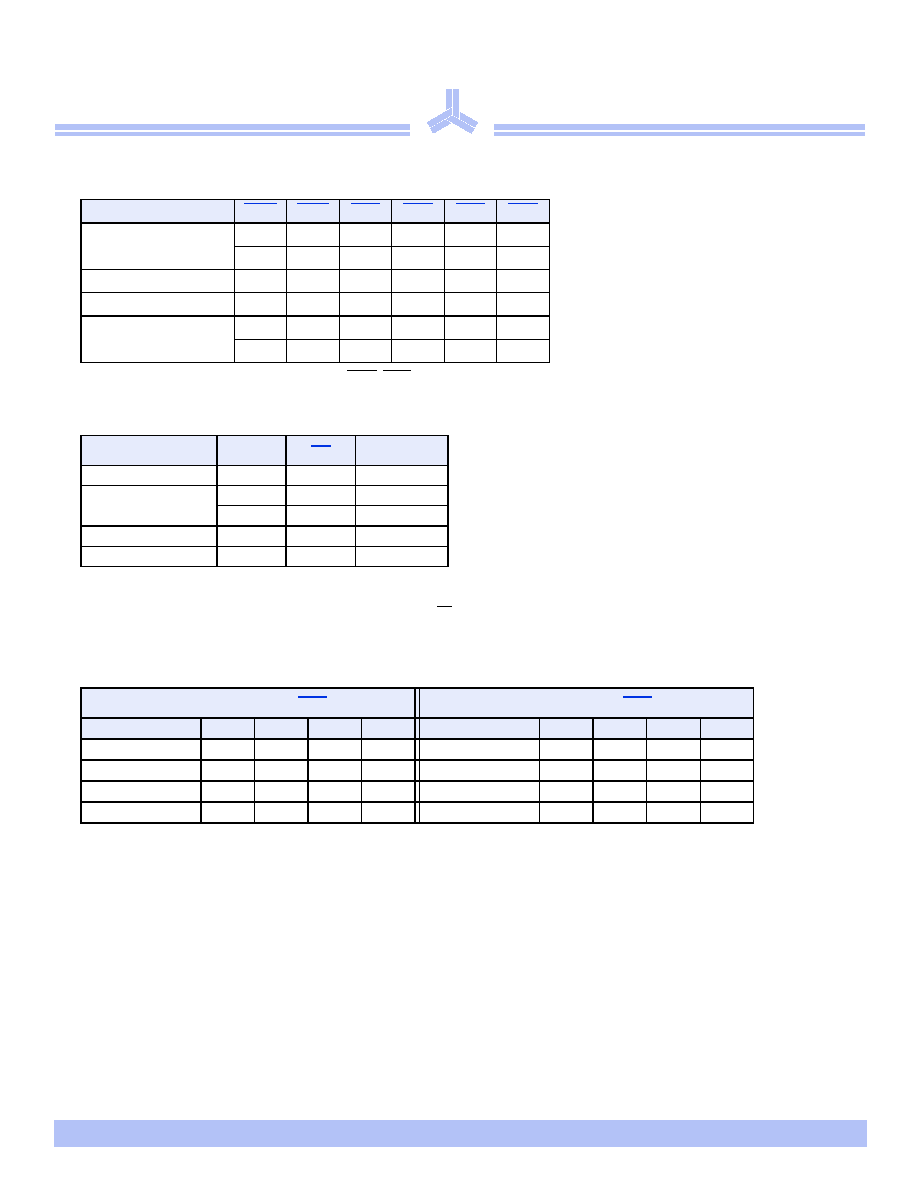
4 Mb Synchronous SRAM products list
1,2
1 Core Power Supply: VDD = 3.3V + 0.165V
2 I/O Supply Voltage: VDDQ = 3.3V + 0.165V for 3.3V I/O
VDDQ = 2.5V + 0.125V for 2.5V I/O
PL-SCD
:
Pipelined Burst Synchronous SRAM - Single Cycle Deselect
PL-DCD
:
Pipelined Burst Synchronous SRAM - Double Cycle Deselect
FT
:
Flow-through Burst Synchronous SRAM
NTD
1
-PL
:
Pipelined Burst Synchronous SRAM with NTD
TM
NTD-FT
:
Flow-through Burst Synchronous SRAM with NTD
TM
Org
Part Number
Mode
Speed
256KX18
AS7C33256PFS18B
PL-SCD
200/166/133 MHz
128KX32
AS7C33128PFS32B
PL-SCD
200/166/133 MHz
128KX36
AS7C33128PFS36B
PL-SCD
200/166/133 MHz
256KX18
AS7C33256PFD18B
PL-DCD
200/166/133 MHz
128KX32
AS7C33128PFD32B
PL-DCD
200/166/133 MHz
128KX36
AS7C33128PFD36B
PL-DCD
200/166/133 MHz
256KX18
AS7C33256FT18B
FT
6.5/7.5/8.0/10 ns
128KX32
AS7C33128FT32B
FT
6.5/7.5/8.0/10 ns
128KX36
AS7C33128FT36B
FT
6.5/7.5/8.0/10 ns
256KX18
AS7C33256NTD18B
NTD-PL
200/166/133 MHz
128KX32
AS7C33128NTD32B
NTD-PL
200/166/133 MHz
128KX36
AS7C33128NTD36B
NTD-PL
200/166/133 MHz
256KX18
AS7C33256NTF18B
NTD-FT
6.5/7.5/8.0/10 ns
128KX32
AS7C33128NTF32B
NTD-FT
6.5/7.5/8.0/10 ns
128KX36
AS7C33128NTF36B
NTD-FT
6.5/7.5/8.0/10 ns
1. NTD: No Turnaround Delay. NTD
TM
is a trademark of Alliance Semiconductor Corporation. All trademarks mentioned in this document are the property
of their respective owners.
Æ
AS7C33128FT32B
2/8/05; v.1.2
Alliance Semiconductor
P. 3 of 19
AS7C33128FT36B
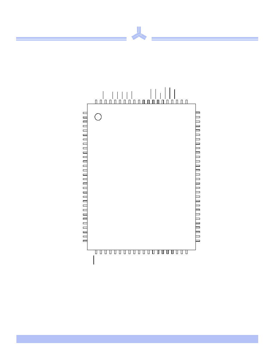
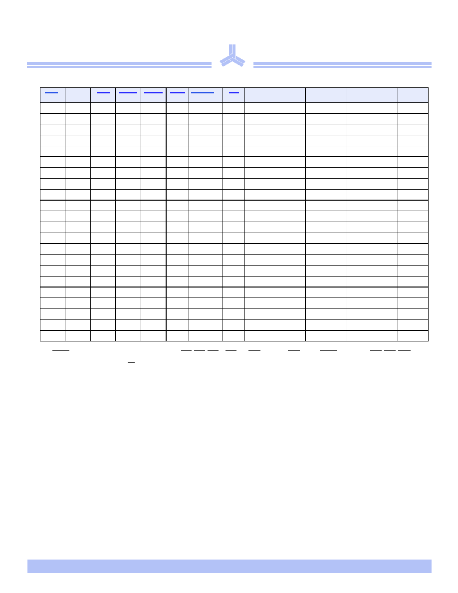
Pin arrangement
DQP
c
/NC
DQ
c0
DQ
c1
V
DDQ
V
SSQ
DQ
c2
DQ
c3
DQ
c4
DQ
c5
V
SSQ
V
DDQ
DQ
c6
DQ
c7
NC
V
DD
NC
V
SS
DQ
d0
DQ
d1
V
DDQ
V
SSQ
DQ
d2
DQ
d3
DQ
d4
DQ
d5
V
SSQ
V
DDQ
DQ
d6
DQ
d7
DQP
d
/NC
1
2
3
4
5
6
7
8
9
10
11
12
13
14
15
16
17
18
19
20
21
22
23
24
25
26
27
28
29
30
80
79
78
77
76
75
74
73
72
71
70
69
68
67
66
65
64
63
62
61
60
59
58
57
56
55
54
53
52
51
DQP
b
/NC
DQ
b7
DQ
b6
V
DDQ
V
SSQ
DQ
b5
DQ
b4
DQ
b3
DQ
b2
V
SSQ
V
DDQ
DQ
b1
DQ
b0
V
SS
ZZ
DQ
a7
DQ
a6
V
DDQ
V
SSQ
DQ
a5
DQ
a4
DQ
a3
DQ
a2
V
SSQ
V
DDQ
DQ
a1
DQ
a0
DQP
a
/NC
LB
O A A A A A1 A0 NC NC V
SS
V
DD
NC NC
A A A A A A
31 32 33 34 35 36 37 38 39 40 41 42 43 44 45 46 47 48 49 50
100 99 98 97 96 95 94 93 92 91 90 89 88 87 86 85 84 83 82 81
A A CE
0
CE
1
BW
d
BW
c
BW
b
BW
a
CE
2
V
DD
V
SS
CL
K
GW
E
BW
E
OE AD
S
C
AD
S
P
AD
V
A A
NC
VDD
A
TQFP 14 ◊ 20 mm
Note: Pins 1,30,51,80 are NC for ◊32
AS7C33128FT32B
Æ
2/8/05; v.1.2
Alliance Semiconductor
P. 4 of 19
AS7C33128FT36B
Functional description
The AS7C33128FT32B/36B is a high-performance CMOS 4-Mbit synchronous Static Random Access Memory (SRAM) device organized
as 131,072 words ◊ 32 or 36 bits.
Fast cycle times of 7.5/8.5/10/12 ns with clock access times (t
CD
) of 6.5/7.5/8.0/10 ns. Three chip enable (CE) inputs permit easy memory
expansion. Burst operation is initiated in one of two ways: the controller address strobe (ADSC), or the processor address strobe (ADSP).
The burst advance pin (ADV) allows subsequent internally generated burst addresses.
Read cycles are initiated with ADSP (regardless of WE and ADSC) using the new external address clocked into the on-chip address register
when ADSP is sampled low, the chip enables are sampled active, and the output buffer is enabled with OE. In a read operation, the data
accessed by the current address registered in the address registers by the positive edge of CLK are carried to the data-out buffer. ADV is
ignored on the clock edge that samples ADSP asserted, but is sampled on all subsequent clock edges. Address is incremented internally for
the next access of the burst when ADV is sampled low and both address strobes are high. Burst mode is selectable with the LBO input. With
LBO unconnected or driven high, burst operations use an interleaved count sequence. With LBO driven low, the device uses a linear count
sequence.
Write cycles are performed by disabling the output buffers with OE and asserting a write command. A global write enable GWE writes all
32/36 regardless of the state of individual BW[a:d] inputs. Alternately, when GWE is high, one or more bytes may be written by asserting
BWE and the appropriate individual byte BWn signals.
BWn is ignored on the clock edge that samples ADSP low, but it is sampled on all subsequent clock edges. Output buffers are disabled when
BWn is sampled LOW regardless of OE. Data is clocked into the data input register when BWn is sampled low. Address is incremented
internally to the next burst address if BWn and ADV are sampled low.
Read or write cycles may also be initiated with ADSC instead of ADSP. The differences between cycles initiated with ADSC and ADSP are
as follows:
∑ ADSP must be sampled high when ADSC is sampled low to initiate a cycle with ADSC.
∑ WE signals are sampled on the clock edge that samples ADSC low (and ADSP high).
∑ Master chip enable CE0 blocks ADSP, but not ADSC.
The AS7C33128FT32B and AS7C33128FT36B family operates from a core 3.3V power supply. I/Os use a separate power supply that can
operate at 2.5V or 3.3V. These devices are available in a 100-pin TQFP package.
TQFP capacitance
*Guaranteed not tested
TQFP thermal resistance
Parameter
Symbol
Test conditions
Min
Max
Unit
Input capacitance
C
IN
*
V
IN
= 0V
-
5
pF
I/O capacitance
C
I/O
*
V
OUT
= 0V
-
7
pF
Description
Conditions
Symbol
Typical
Units
Thermal resistance
(junction to ambient)
1
1 This parameter is sampled
Test conditions follow standard test methods and
procedures for measuring thermal impedance,
per EIA/JESD51
1≠layer
JA
40
∞C/W
4≠layer
JA
22
∞C/W
Thermal resistance
(junction to top of case)
1
JC
8
∞C/W
Æ
AS7C33128FT32B
2/8/05; v.1.2
Alliance Semiconductor
P. 5 of 19
AS7C33128FT36B
Signal descriptions
Snooze Mode
SNOOZE MODE is a low current, power-down mode in which the device is deselected and current is reduced to I
SB2
. The duration of
SNOOZE MODE is dictated by the length of time the ZZ is in a High state.
The ZZ pin is an asynchronous, active high input that causes the device to enter SNOOZE MODE.
When the ZZ pin becomes a logic High, I
SB2
is guaranteed after the time t
ZZI
is met. After entering SNOOZE MODE, all inputs except ZZ
is disabled and all outputs go to High-Z. Any operation pending when entering SNOOZE MODE is not guaranteed to successfully complete.
Therefore, SNOOZE MODE (READ or WRITE) must not be initiated until valid pending operations are completed. Similarly, when exiting
SNOOZE MODE during t
PUS
, only a DESELECT or READ cycle should be given while the SRAM is transitioning out of SNOOZE MODE.
Pin
I/O
Properties
Description
CLK
I
CLOCK
Clock. All inputs except OE, ZZ, and LBO are synchronous to this clock.
A,A0,A1
I
SYNC
Address. Sampled when all chip enables are active and when ADSC or ADSP are asserted.
DQ[a,b,c,d]
I/O
SYNC
Data. Driven as output when the chip is enabled and when OE is active.
CE0
I
SYNC
Master chip enable. Sampled on clock edges when ADSP or ADSC is active. When CE0 is inactive,
ADSP is blocked. Refer to the "Synchronous truth table" for more information.
CE1, CE2
I
SYNC
Synchronous chip enables, active high, and active low, respectively. Sampled on clock edges when
ADSC is active or when CE0 and ADSP are active.
ADSP
I
SYNC
Address strobe processor. Asserted low to load a new address or to enter standby mode.
ADSC
I
SYNC
Address strobe controller. Asserted low to load a new address or to enter standby mode.
ADV
I
SYNC
Advance. Asserted low to continue burst read/write.
GWE
I
SYNC
Global write enable. Asserted low to write all 32/36 bits. When high, BWE and BW[a:d] control write
enable.
BWE
I
SYNC
Byte write enable. Asserted low with GWE high to enable effect of BW[a:d] inputs.
BW[a,b,c,d]
I
SYNC
Write enables. Used to control write of individual bytes when GWE is high and BWE is low. If any of
BW[a:d] is active with GWE high and BWE low, the cycle is a write cycle. If all BW[a:d] are inactive,
the cycle is a read cycle.
OE
I
ASYNC
Asynchronous output enable. I/O pins are driven when OE is active and chip is in read mode.
LBO
I
STATIC
Selects Burst mode. When tied to V
DD
or left floating, device follows interleaved Burst order. When
driven Low, device follows linear Burst order. This signal is internally pulled High.
ZZ
I
ASYNC
Snooze. Places device in low power mode; data is retained. Connect to GND if unused.
NC
-
-
No connect
AS7C33128FT32B
Æ
2/8/05; v.1.2
Alliance Semiconductor
P. 6 of 19
AS7C33128FT36B
Asynchronous Truth Table
Notes:
1. X means "Don't Care"
2. ZZ pin is pulled down internally
3. For write cycles that follows read cycles, the output buffers must be disabled with OE, otherwise data bus contention will occur.
4. Snooze mode means power down state of which stand-by current does not depend on cycle times
5. Deselected means power down state of which stand-by current depends on cycle times
Burst sequence table
Write enable truth table (per byte)
1
1
Key: X = don't care, L = low, H = high, n = a, b, c, d;
BWE
,
BWn
= internal write signal.
Function
GWE
BWE
BWa
BWb
BWc
BWd
Write All Bytes
L
X
X
X
X
X
H
L
L
L
L
L
Write Byte a
H
L
L
H
H
H
Write Byte c and d
H
L
H
H
L
L
Read
H
H
X
X
X
X
H
L
H
H
H
H
Operation
ZZ
OE
I/O Status
Snooze mode
H
X
High-Z
Read
L
L
Dout
L
H
High-Z
Write L
X
Din,
High-Z
Deselected
L
X
High-Z
Interleaved burst address (LBO = 1)
Linear burst address (LBO = 0)
A1 A0
A1 A0
A1 A0
A1 A0
A1 A0
A1 A0
A1 A0
A1 A0
1
st
Address
0 0
0 1
1 0
1 1
1
st
Address
0 0
0 1
1 0
1 1
2
nd
Address
0 1
0 0
1 1
1 0
2
nd
Address
0 1
1 0
1 1
0 0
3
rd
Address
1 0
1 1
0 0
0 1
3
rd
Address
1 0
1 1
0 0
0 1
4
th
Address
1 1
1 0
0 1
0 0
4
th
Address
1 1
1 0
0 1
1 0
Æ
AS7C33128FT32B
2/8/05; v.1.2
Alliance Semiconductor
P. 7 of 19
AS7C33128FT36B
Synchronous truth table
[4]
CE0
1
1 X = don't care, L = low, H = high
CE1
CE2
ADSP ADSC ADV
WRITE
[2]
2 For WRITE, L means any one or more byte write enable signals (BWa, BWb, BWc or BWd) and BWE are LOW or GWE is LOW. WRITE = HIGH for all BWx, BWE, GWE
HIGH. See "Write enable truth table (per byte)," on page 6 for more information.
OE
Address accessed
CLK
Operation
DQ
H
X
X
X
L
X
X
X
NA
L to H
Deselect
Hi
-Z
L
L
X
L
X
X
X
X
NA
L to H
Deselect
Hi
-Z
L
L
X
H
L
X
X
X
NA
L to H
Deselect
Hi
-Z
L
X
H
L
X
X
X
X
NA
L to H
Deselect
Hi
-Z
L
X
H
H
L
X
X
X
NA
L to H
Deselect
Hi
-Z
L
H
L
L
X
X
X
L
External
L to H
Begin read
Q
L
H
L
L
X
X
X
H
External
L to H
Begin read
Hi
-Z
L
H
L
H
L
X
H
L
External
L to H
Begin read
Q
L
H
L
H
L
X
H
H
External
L to H
Begin read
Hi
-Z
X
X
X
H
H
L
H
L
Next
L to H
Continue read
Q
X
X
X
H
H
L
H
H
Next
L to H
Continue read
Hi
-Z
X
X
X
H
H
H
H
L
Current
L to H
Suspend read
Q
X
X
X
H
H
H
H
H
Current
L to H
Suspend read
Hi
-Z
H
X
X
X
H
L
H
L
Next
L to H
Continue read
Q
H
X
X
X
H
L
H
H
Next
L to H
Continue read
Hi
-Z
H
X
X
X
H
H
H
L
Current
L to H
Suspend read
Q
H
X
X
X
H
H
H
H
Current
L to H
Suspend read
Hi
-Z
L
H
L
H
L
X
L
X
External
L to H
Begin write
D
3
3 For write operation following a READ, OE must be high before the input data set up time and held high throughout the input hold time
4 ZZ pin is always Low.
X
X
X
H
H
L
L
X
Next
L to H
Continue write
D
H
X
X
X
H
L
L
X
Next
L to H
Continue write
D
X
X
X
H
H
H
L
X
Current
L to H
Suspend write
D
H
X
X
X
H
H
L
X
Current
L to H
Suspend write
D
AS7C33128FT32B
Æ
2/8/05; v.1.2
Alliance Semiconductor
P. 8 of 19
AS7C33128FT36B
Note: Stresses greater than those listed under Absolute Maximum Ratings may cause permanent damage to the device. This is a stress rating only and functional operation of the device at these or any other con-
ditions outside those indicated in the operational sections of this specification is not implied. Exposure to absolute maximum rating conditions may affect reliability.
Recommended operating conditions at 3.3V I/O
Recommended operating conditions at 2.5V I/O
Absolute maximum ratings
Parameter
Symbol
Min
Max
Unit
Power supply voltage relative to GND
V
DD
, V
DDQ
≠0.5
+4.6
V
Input voltage relative to GND (input pins)
V
IN
≠0.5
V
DD
+ 0.5
V
Input voltage relative to GND (I/O pins)
V
IN
≠0.5
V
DDQ
+ 0.5
V
Power dissipation
P
D
≠
1.8
W
DC output current
I
OUT
≠
50
mA
Storage temperature (plastic)
T
stg
≠65
+150
∞C
Temperature under bias
T
bias
≠65 +135
∞C
Parameter
Symbol
Min
Nominal
Max
Unit
Supply voltage for inputs
V
DD
3.135
3.3
3.465
V
Supply voltage for I/O
V
DDQ
3.135
3.3
3.465
V
Ground supply
Vss
0
0
0
V
Parameter
Symbol
Min
Nominal
Max
Unit
Supply voltage for inputs
V
DD
3.135
3.3
3.465
V
Supply voltage for I/O
V
DDQ
2.375
2.5
2.625
V
Ground supply
Vss
0
0
0
V
Æ
AS7C33128FT32B
2/8/05; v.1.2
Alliance Semiconductor
P. 9 of 19
AS7C33128FT36B
DC electrical characteristics for 3.3V I/O operation
DC electrical characteristics for 2.5V I/O operation
LBO and ZZ pins have an internal pull-up or pull-down, and input leakage = ±10
µA.
*
V
IH
max < VDD +1.5V for pulse width less than 0.2 X t
CYC
**
V
IL
min = -1.5 for pulse width less than 0.2 X t
CYC
I
DD
operating conditions and maximum limits
Parameter
Sym
Conditions
Min
Max
Unit
Input leakage current
|I
LI
|
V
DD
= Max, 0V < V
IN
< V
DD
-2
2
µA
Output leakage current
|I
LO
|
OE
V
IH
, V
DD
= Max, 0V < V
OUT
< V
DDQ
-2
2
µA
Input high (logic 1) voltage
V
IH
Address and control pins
2*
V
DD
+0.3
V
I/O pins
2*
V
DDQ
+0.3
Input low (logic 0) voltage
V
IL
Address and control pins
-0.3**
0.8
V
I/O pins
-0.5**
0.8
Output high voltage
V
OH
I
OH
= ≠4 mA, V
DDQ
= 3.135V
2.4
≠
V
Output low voltage
V
OL
I
OL
= 8 mA, V
DDQ
= 3.465V
≠
0.4
V
Parameter
Sym
Conditions
Min
Max
Unit
Input leakage current
|I
LI
|
V
DD
= Max, 0V < V
IN
< V
DD
-2
2
µA
Output leakage current
|I
LO
|
OE
V
IH
, V
DD
= Max, 0V < V
OUT
< V
DDQ
-2
2
µA
Input high (logic 1) voltage
V
IH
Address and control pins
1.7*
V
DD
+0.3
V
I/O pins
1.7*
V
DDQ
+0.3
V
Input low (logic 0) voltage
V
IL
Address and control pins
-0.3**
0.7
V
I/O pins
-0.3**
0.7
V
Output high voltage
V
OH
I
OH
= ≠4 mA, V
DDQ
= 2.375V
1.7
≠
V
Output low voltage
V
OL
I
OL
= 8 mA, V
DDQ
= 2.625V
≠
0.7
V
Parameter
Sym
Conditions
-65
-75
-80
-10
Unit
Operating power supply current
1
1 I
CC
given with no output loading. I
CC
increases with faster cycle times and greater output loading.
I
CC
CE0 < V
IL
, CE1 > V
IH
, CE2 < V
IL
, f = f
Max
,
I
OUT
= 0 mA, ZZ
< V
IL
275
250
215
185
mA
Standby power supply current
I
SB
All V
IN
0.2V or > V
DD
≠ 0.2V, Deselected,
f = f
Max
, ZZ
< V
IL
90
85
75
75
mA
I
SB1
Deselected, f = 0, ZZ
< 0.2V,
all V
IN
0.2V or V
DD
≠ 0.2V
30
30
30
30
I
SB2
Deselected, f = f
Max
, ZZ
V
DD
≠ 0.2V,
all V
IN
V
IL
or
V
IH
30
30
30
30
AS7C33128FT32B
Æ
2/8/05; v.1.2
Alliance Semiconductor
P. 10 of 19
AS7C33128FT36B
Snooze Mode Electrical Characteristics
Timing characteristics over operating range
Parameter
Sym
≠65
-75
-80
≠10
Unit
Notes
1
1
See "Notes" on page 16.
Min Max Min Max Min Max
Min
Max
Cycle time
t
CYC
7.5
≠
8.5
≠
10
≠
12
≠
ns
Clock access time
t
CD
≠
6.5
≠
7.5
≠
8.0
≠
10
ns
Output enable LOW to data valid
t
OE
≠
3.5
≠
3.5
≠
4.0
≠
4.0
ns
Clock HIGH to output Low Z
t
LZC
2.5
≠
2.5
≠
2.5
≠
2.5
≠
ns
2,3,4
Data output invalid from clock HIGH
t
OH
2.5
≠
2.5
≠
2.5
≠
2.5
≠
ns
2
Output enable LOW to output Low Z
t
LZOE
0
≠
0
≠
0
≠
0
≠
ns
2,3,4
Output enable HIGH to output High Z
t
HZOE
≠
3.0
≠
3.5
≠
4.0
≠
5.0
ns
2,3,4
Clock HIGH to output High Z
t
HZC
≠
3.0
≠
3.5
≠
4.0
≠
5.0
ns
2,3,4
Output enable HIGH to invalid output
t
OHOE
0
≠
0
≠
0
≠
0
≠
ns
Clock HIGH pulse width
t
CH
2.5
≠
3.0
≠
4.0
≠
4.0
≠
ns
5
Clock LOW pulse width
t
CL
2.5
≠
3.0
≠
4.0
≠
4.0
≠
ns
5
Address setup to clock HIGH
t
AS
1.5
≠
2.0
≠
2.0
≠
2.0
≠
ns
6
Data setup to clock HIGH
t
DS
1.5
≠
2.0
≠
2.0
≠
2.0
≠
ns
6
Write setup to clock HIGH
t
WS
1.5
≠
2.0
≠
2.0
≠
2.0
≠
ns
6,7
Chip select setup to clock HIGH
t
CSS
1.5
≠
2.0
≠
2.0
≠
2.0
≠
ns
6,8
Address hold from clock HIGH
t
AH
0.5
≠
0.5
≠
0.5
≠
0.5
≠
ns
6
Data hold from clock HIGH
t
DH
0.5
≠
0.5
≠
0.5
≠
0.5
≠
ns
6
Write hold from clock HIGH
t
WH
0.5
≠
0.5
≠
0.5
≠
0.5
≠
ns
6,7
Chip select hold from clock HIGH
t
CSH
0.5
≠
0.5
≠
0.5
≠
0.5
≠
ns
6,8
ADV setup to clock HIGH
t
ADVS
1.5
≠
2.0
≠
2.0
≠
2.0
≠
ns
6
ADSP setup to clock HIGH
t
ADSPS
1.5
≠
2.0
≠
2.0
≠
2.0
≠
ns
6
ADSC setup to clock HIGH
t
ADSCS
1.5
≠
2.0
≠
2.0
≠
2.0
≠
ns
6
ADV hold from clock HIGH
t
ADVH
0.5
≠
0.5
≠
0.5
≠
0.5
≠
ns
6
ADSP hold from clock HIGH
t
ADSPH
0.5
≠
0.5
≠
0.5
≠
0.5
≠
ns
6
ADSC hold from clock HIGH
t
ADSCH
0.5
≠
0.5
≠
0.5
≠
0.5
≠
ns
6
Description
Conditions
Symbol
Min
Max
Units
Current during Snooze Mode
ZZ > V
IH
I
SB2
30
mA
ZZ active to input ignored
t
PDS
2
cycle
ZZ inactive to input sampled
t
PUS
2
cycle
ZZ active to SNOOZE current
t
ZZI
2
cycle
ZZ inactive to exit SNOOZE current
t
RZZI
0
Æ
AS7C33128FT32B
2/8/05; v.1.2
Alliance Semiconductor
P. 11 of 19
AS7C33128FT36B
Key to switching waveforms
Timing waveform of read cycle
Note: ð = XOR when LBO = high/no connect; ð = ADD when LBO = low. BW[a:d] is don't care.
don't care
Falling input
Rising input
Undefined
t
CYC
t
CH
t
CL
t
ADSPS
t
ADSPH
t
AS
t
AH
t
WS
t
ADVS
t
OH
CLK
ADSP
ADSC
Address
GWE, BWE
CE0, CE2
ADV
OE
t
CSS
t
CD
t
WH
t
ADVH
t
HZOE
t
ADSCS
t
ADSCH
LOAD NEW ADDRESS
ADV inserts wait states
A2
A1
A3
Dout
Q(A2ð10)
Q(A2ð11)
Q(A3)
Q(A2ð01)
Q(A3ð01)
Q(A3ð10)
Q(A3ð11)
Q(A1)
t
HZC
t
LZOE
t
CSH
Read
Q(A1)
Suspend
Read
Q(A1)
Read
Q(A2)
Burst Read
Q(A 2ð01)
Read
Q(A3)
DSEL
Burst Read
Q(A 2ð10)
Suspend
Read
Q(A 2ð10)
Burst Read
Q(A 2ð11)
Burst Read
Q(A 3ð01)
Burst Read
Q(A 3ð10)
Burst Read
Q(A 3ð11)
t
OE
CE1
AS7C33128FT32B
Æ
2/8/05; v.1.2
Alliance Semiconductor
P. 12 of 19
AS7C33128FT36B
Timing waveform of write cycle
Note: ð = XOR when LBO = high/no connect; ð = ADD when LBO = low.
t
CYC
t
CL
t
ADSPS
t
ADSPH
t
ADSCS
t
ADSCH
t
AS
t
AH
t
WS
t
WH
t
CSS
t
ADVS
t
DS
t
DH
CLK
ADSP
ADSC
Address
BWE
CE0, CE2
ADV
OE
Din
t
CSH
t
ADVH
D(A2ð01)
D(A2ð10)
D(A3)
D(A2)
D(A2ð01)
D(A3ð01)
D(A3ð10)
D(A1)
D(A2ð11)
ADV SUSPENDS BURST
ADSC LOADS NEW ADDRESS
A1
A2
A3
t
CH
CE1
BW[a:d]
Read
Q(A1)
Suspend
Write
D(A1)
Read
Q(A2)
Suspend
Write
D(A 2)
ADV
Burst
Write
D(A 2ð01)
Suspend
Write
D(A 2ð01)
ADV
Burst
Write
D(A 2ð10)
Write
D(A 3)
Burst
Write
D(A 3ð01)
ADV
Burst
Write
D(A 2ð11)
ADV
Burst
Write
D(A 3ð10)
Æ
AS7C33128FT32B
2/8/05; v.1.2
Alliance Semiconductor
P. 13 of 19
AS7C33128FT36B
Timing waveform of read/write cycle (ADSP Controlled; ADSC High)
Note: ð = XOR when LBO = high/no connect; ð = ADD when LBO = low.
t
CH
t
CYC
t
CL
t
ADSPS
t
ADSPH
t
AS
t
AH
t
WS
t
WH
t
ADVS
t
DS
t
DH
t
OH
CLK
ADSP
Address
BWE
CE0, CE2
ADV
OE
Din
Dout
t
CD
t
ADVH
t
LZOE
t
OE
t
LZC
Q(A1)
Q(A3ð01)
D(A2)
Q(A3)
Q(A3ð10)
Q(A3ð11)
A1
A2
A3
CE1
t
HZOE
Suspend
Read
Q(A1)
Read
Q(A1)
Suspend
Write
D(A 2)
ADV
Burst
Read
Q(A 3ð01)
Suspend
Read
Q(A 3ð11)
ADV
Burst
Read
Q(A 3ð10)
ADV
Burst
Read
Q(A 3ð11)
Read
Q(A2)
Read
Q(A3)
BW[a:d]
Æ
AS7C33128FT32B
2/8/05; v.1.2
Alliance Semiconductor
P. 14 of 19
AS7C33128FT36B
Timing waveform of read/write cycle(ADSC controlled, ADSP = HIGH)
Note: ADV is don't care here.
t
CYC
t
CH
t
CL
t
ADSCH
CLK
ADSC
ADDRESS
A2
A1
t
ADSCS
A3
A4
A6
A5
A7
A8
A9
t
AH
t
AS
BWE
t
WH
t
WS
t
CSH
CE0,CE2
t
CSS
t
LZOE
t
OE
t
HZOE
Q(A1)
Q(A2)
Q(A3)
Q(A4)
Q(A9)
Q(A10)
t
CD
t
OH
D(A6)
D(A7)
D(A5)
t
DS
t
DH
OE
Dout
Din
READ
Q(A1)
READ
Q(A2)
READ
Q(A3)
READ
Q(A4)
WRITE
D(A5)
WRITE
D(A6)
WRITE
D(A7)
WRITE
D(A8)
READ
Q(A10)
CE1
A10
D(A8)
READ
Q(A9)
BW[a:d]
Æ
AS7C33128FT32B
2/8/05; v.1.2
Alliance Semiconductor
P. 15 of 19
AS7C33128FT36B
Timing waveform of power down cycle
t
CYC
t
CH
t
CL
t
ADSPS
CLK
ADSP
ADDRESS
A1
t
ADSPS
A2
BWE
t
WH
t
WS
t
CSH
CE0,CE2
t
CSS
ADV
t
LZOE
t
OE
t
HZOE
Q(A1)
Q(A2)
OE
Dout
Din
ADSC
t
HZC
t
PDS
Sleep
ZZ Setup Cycle
t
PUS
ZZ Recovery Cycle
Normal Operation Mode
CE1
ZZ
Q(A2(ð01))
BW[a:d]
READ
Q(A1)
READ
Q(A1ð01)
READ
Q(A2)
READ
Q(A2ð01)
State
t
ZZI
I
SB2
t
RZZI
I
supply
Æ
AS7C33128FT32B
2/8/05; v.1.2
Alliance Semiconductor
P. 16 of 19
AS7C33128FT36B
AC test conditions
Z
0
= 50
D
OUT
50
Figure B: Output load (A)
30 pF*
Figure A: Input waveform
10%
90%
GND
90%
10%
+3.0V
∑ Output load: see Figure B, except for t
LZC
, t
LZOE
, t
HZOE
, t
HZC
, see Figure C.
∑ Input pulse level: GND to 3V. See Figure A.
∑ Input rise and fall time (measured at 0.3V and 2.7V): 2 ns. See Figure A.
∑ Input and output timing reference levels: 1.5V.
V
L
= 1.5V
for 3.3V I/O;
= V
DDQ
/2
for 2.5V I/O
353
/ 1538
5 pF*
319
/ 1667
D
OUT
GND
Figure C: Output load (B)
*including scope
and jig capacitanc
Thevenin equivalent:
+3.3V for 3.3V I/O;
/+2.5V for 2.5V I/O
Notes
1
For test conditions, see AC Test Conditions, Figures A, B, C.
2
This parameter measured with output load condition in Figure C.
3
This parameter is sampled, but not 100% tested.
4
t
HZOE
is less than t
LZOE
; and t
HZC
is less than t
LZC
at any given temperature and voltage.
5
tCH measured as HIGH above VIH and tCL measured as LOW below VIL.
6
This is a synchronous device. All addresses must meet the specified setup and hold times for all rising edges of CLK. All other synchronous inputs
must meet the setup and hold times for all rising edges of CLK when chip is enabled.
7
Write refers to
GWE, BWE, BW[a:d].
8
Chip select refers to
CE0, CE1, CE2
Æ
AS7C33128FT32B
2/8/05; v.1.2
Alliance Semiconductor
P. 17 of 19
AS7C33128FT36B
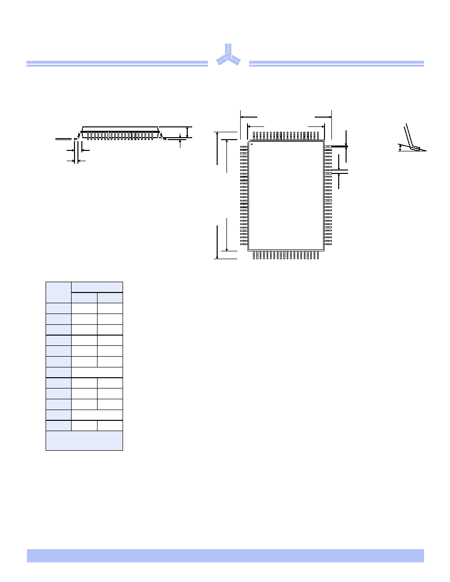
Package Dimensions
100-pin quad flat pack (TQFP)
TQFP
Min
Max
A1
0.05
0.15
A2
1.35
1.45
b
0.22
0.38
c
0.09
0.20
D
13.90
14.10
E
19.90
20.10
e
0.65 nominal
Hd
15.85
16.15
He
21.80
22.20
L
0.45
0.75
L1
1.00 nominal
0∞
7∞
Dimensions in
millimeters
He E
Hd
D
b
e
A1 A2
L1
L
c
Æ
AS7C33128FT32B
2/8/05; v.1.2
Alliance Semiconductor
P. 18 of 19
AS7C33128FT36B
Note: Add suffix `N' to the above part numbers for Lead Free Parts (Ex.
AS7C33128FT32B-65TQCN)
1. Alliance Semiconductor SRAM Prefix
2. Operating voltage: 33 = 3.3V
3. Organization: 128 = 128K
4. Flowthrough mode
5. Organization: 32 = X32; 36 = X36
6. Production version: B= product revision
7. Clock access time: [-65 = 6.5 ns; -75 = 7.5 ns; -80 = 8.0 ns; -10 = 10.0]
8. Package type: TQ = TQFP
9. Operating temperature: C = Commercial (0∞ C to 70∞ C); I = Industrial (-40∞ C to 85∞ C)
10. N = Lead free part
Ordering information
Package Width
≠65
-75
≠80
≠10
TQFP
x32
AS7C33128FT32B-
65TQC
AS7C33128FT32B-
75TQC
AS7C33128FT32B-
80TQC
AS7C33128FT32B-
10TQC
TQFP
x32
AS7C33128FT32B-
65TQI
AS7C33128FT32B-
75TQI
AS7C33128FT32B-
80TQI
AS7C33128FT32B-
10TQI
TQFP
x36
AS7C33128FT36B-
65TQC
AS7C33128FT36B-
75TQC
AS7C33128FT36B-
80TQC
AS7C33128FT36B-
10TQC
TQFP
x36
AS7C33128FT36B-
65TQI
AS7C33128FT36B-
75TQI
AS7C33128FT36B-
80TQI
AS7C33128FT36B-
10TQI
Part numbering guide
AS7C
33
128
FT
32/36
B
≠XX
TQ
C/I
X
1
2
3
4
5
6
7
8
9
10

AS7C33128FT32B
Æ
© Copyright 2003 Alliance Semiconductor Corporation. All rights reserved. Our three-point logo, our name and Intelliwatt are trademarks or registered
trademarks of Alliance. All other brand and product names may be the trademarks of their respective companies. Alliance reserves the right to make
changes to this document and its products at any time without notice. Alliance assumes no responsibility for any errors that may appear in this document.
The data contained herein represents Alliance's best data and/or estimates at the time of issuance. Alliance reserves the right to change or correct this data at
any time, without notice. If the product described herein is under development, significant changes to these specifications are possible. The information in
this product data sheet is intended to be general descriptive information for potential customers and users, and is not intended to operate as, or provide, any
guarantee or warrantee to any user or customer. Alliance does not assume any responsibility or liability arising out of the application or use of any product
described herein, and disclaims any express or implied warranties related to the sale and/or use of Alliance products including liability or warranties related
to fitness for a particular purpose, merchantability, or infringement of any intellectual property rights, except as express agreed to in Alliance's Terms and
Conditions of Sale (which are available from Alliance). All sales of Alliance products are made exclusively according to Alliance's Terms and Conditions of
Sale. The purchase of products from Alliance does not convey a license under any patent rights, copyrights; mask works rights, trademarks, or any other
intellectual property rights of Alliance or third parties. Alliance does not authorize its products for use as critical components in life-supporting systems
where a malfunction or failure may reasonably be expected to result in significant injury to the user, and the inclusion of Alliance products in such life-
supporting systems implies that the manufacturer assumes all risk of such use and agrees to indemnify Alliance against all claims arising from such use.
Alliance Semiconductor Corporation
2575, Augustine Drive,
Santa Clara, CA 95054
Tel: 408 - 855 - 4900
Fax: 408 - 855 - 4999
www.alsc.com
Copyright © Alliance Semiconductor
All Rights Reserved
Part Number: AS7C33128FT32B
AS7C33128FT36B
Document Version: v.1.2
Æ
AS7C33128FT36B