AS7C33512NTD32-36A.V032003.fm
March 2003
Advance Information
&RS\ULJKW $OOLDQFH 6HPLFRQGXFWRU $OO ULJKWV UHVHUYHG
AS7C33512NTD32A
AS7C33512NTD36A
9 $GYDQFH ,QIR
$OOLDQFH 6HPLFRQGXFWRU
3 RI
9 . î 65$0 ZLWK 17'
TM
Features
· Organization: 524,288 words × 32 or 36 bits
· NTD
TM1
architecture for efficient bus operation
· Fast clock speeds to 200 MHz in LVTTL/LVCMOS
· Fast clock to data access: 3/3.4/3.8 ns
· Fast OE access time:
3/3.4/3.8 ns
· Fully synchronous operation
· Flow-through or pipelined mode
· Asynchronous output enable control
1. NTD
TM
is a trademark of Alliance Semiconductor Corporation.
· Available in 100-pin TQFP and 165-ball BGA package
· Byte write enables
· Clock enable for operation hold
· Multiple chip enables for easy expansion
· 3.3V core power supply
· 2.5V or 3.3V I/O operation with separate V
DDQ
· Self-timed write cycles
· Interleaved or linear burst modes
· Snooze mode for standby operation
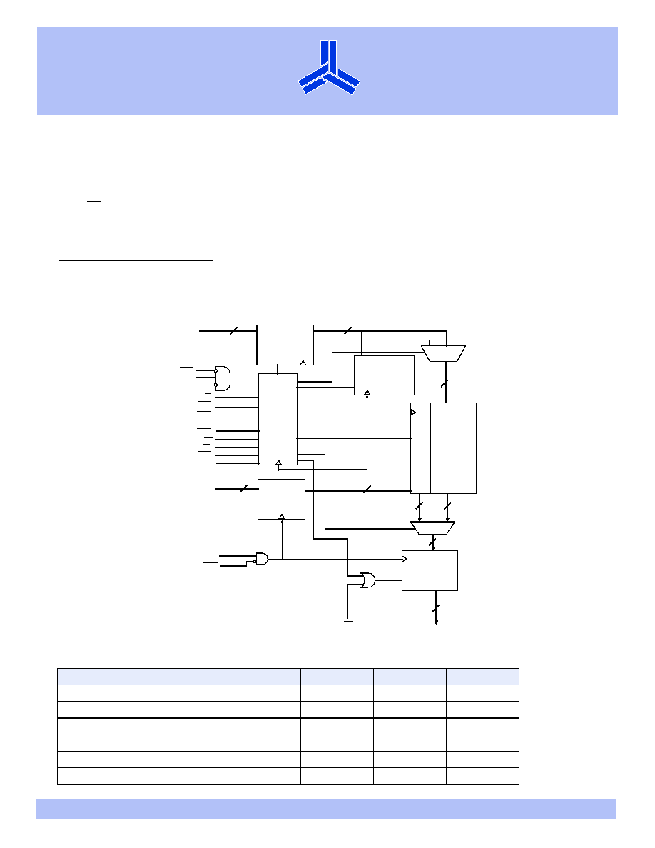
Logic block diagram
Selection guide
-200
-166
-133
Units
Minimum cycle time
5
6
7.5
ns
Maximum pipelined clock frequency
200
166
133
MHz
Maximum pipelined clock access time
3.0
3.4
3.8
ns
Maximum operating current
400
350
325
mA
Maximum standby current
130
120
110
mA
Maximum CMOS standby current (DC)
70
70
70
mA
:U
L
W
H
%
X
I
I
H
U
$GGUHVV
'
4
&/.
UHJLVWHU
2XWSXW
5HJLVWHU
'4>DEFG@
&/.
&(
&(
&(
$>@
2(
&/.
&(1
&RQWURO
&/.
ORJLF
'DWD
'
4
&/.
,QSXW
5HJLVWHU
2(
. [
65$0
$UUD\
5:
'4>DEFG@
%:E
%:G
&/.
4
'
)7
$'9 /'
/%2
%XUVW ORJLF
DGGU UHJLVWHUV
:ULWH GHOD\
==
&/.
%:F
%:D
$6&17'$$
9 $GYDQFH ,QIR
$OOLDQFH 6HPLFRQGXFWRU
3 RI
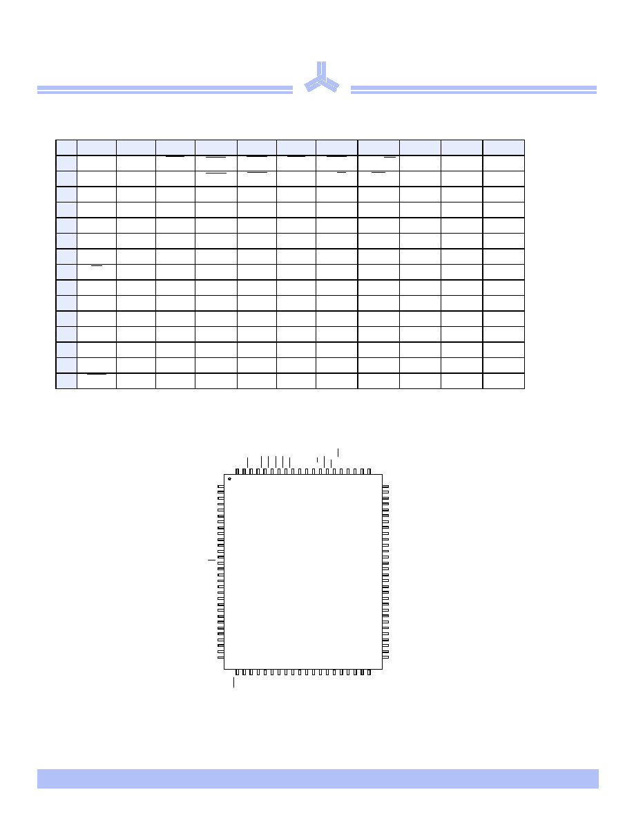
Pin and ball assignment
165-ball BGA - top view
100-pin TQFP - top view
1
2
3
4
5
6
7
8
9
10
11
A
1&
$
&(
%:F
%:E
&(
&(1
ADV/LD
$
$
1&
B
1&
$
&(
%:G
%:D
&/.
5:
2(
$
$
1&
C
'43F
1&
9
''4
9
66
9
66
9
66
9
66
9
66
9
''4
1&
'43E
D
'4F
'4F
9
''4
9
''
9
66
9
66
9
66
9
''
9
''4
'4E
'4E
E
'4F
'4F
9
''4
9
''
9
66
9
66
9
66
9
''
9
''4
'4E
'4E
F
'4F
'4F
9
''4
9
''
9
66
9
66
9
66
9
''
9
''4
'4E
'4E
G
'4F
'4F
9
''4
9
''
9
66
9
66
9
66
9
''
9
''4
'4E
'4E
H
)7
1&
1&
9
''
9
66
9
66
9
66
9
''
1&
1&
==
J
'4G
'4G
9
''4
9
''
9
66
9
66
9
66
9
''
9
''4
'4D
'4D
K
'4G
'4G
9
''4
9
''
9
66
9
66
9
66
9
''
9
''4
'4D
'4D
L
'4G
'4G
9
''4
9
''
9
66
9
66
9
66
9
''
9
''4
'4D
'4D
M
'4G
'4G
9
''4
9
''
9
66
9
66
9
66
9
''
9
''4
'4D
'4D
N
'43G
1&
9
''4
9
66
1&
1&
1&
9
66
9
''4
1&
'43D
P
1&
1&
$
$
7',
$
1 A0 and A1 are the two least significant bits (LSB) of the address field and set the internal burst counter if burst is desired.
7'2
$
$
$
1&
R
/%2
1&
$
$
706
$
7&.
$
$
$
$
/%
2 $ $ $ $ $ $ 1& 1& 9
66
9
''
1& 1&
$ $ $ $ $ $
$ $ &(
&(
%:
G
%:
F
%:
E
%:
D
&(
9
''
9
66
&/. 5
:
&(
1
2( $'
9
/'
$ $ $ $
74)3 [ PP
$
1&' 4 3F
' 4 F
' 4 F
9
''4
9
664
' 4 F
' 4 F
' 4 F
' 4 F
9
664
9
''4
' 4 F
' 4 F
)7
9
''
1&
9
66
' 4 G
' 4 G
9
''4
9
664
' 4 G
' 4 G
' 4 G
' 4 G
9
664
9
''4
' 4 G
' 4 G
1&' 4 3G
' 4 3E1&
' 4 E
' 4 E
9
''4
9
664
' 4 E
' 4 E
' 4 E
' 4 E
9
664
9
''4
' 4 E
' 4 E
9
66
==
' 4 D
' 4 D
9
''4
9
664
' 4 D
' 4 D
' 4 D
' 4 D
9
664
9
''4
' 4 D
' 4 D
' 4 3D1&
9
''
1&
1RWH )RU SLQV DQG 1& DSSOLHV WR WKH [ FRQILJXUDWLRQ
'43Q DSSOLHV WR WKH [ FRQILJXUDWLRQ
$6&17'$$
9 $GYDQFH ,QIR
$OOLDQFH 6HPLFRQGXFWRU
3 RI
Functional description
The AS7C33512NTD32A/36A family is a high performance CMOS 16 Mbit synchronous Static Random Access Memory (SRAM) organized as
524,288 words × 32 or 36 bits and incorporates a LATE LATE Write.
This variation of the 16Mb+ synchronous SRAM uses the No Turnaround Delay (NTD
TM
) architecture, featuring an enhanced write operation
that improves bandwidth over pipelined burst devices. In a normal pipelined burst device, the write data, command, and address are all applied
to the device on the same clock edge. If a read command follows this write command, the system must wait for two 'dead' cycles for valid data
to become available. These dead cycles can significantly reduce overall bandwidth for applications requiring random access or read-modify-
write operations.
NTD
TM
devices use the memory bus more efficiently by introducing a write latency which matches the two-cycle pipelined or one-cycle flow-
through read latency. Write data is applied two cycles after the write command and address, allowing the read pipeline to clear. With NTD
TM
,
write and read operations can be used in any order without producing dead bus cycles.
Assert R/W low to perform write cycles. Byte write enable controls write access to specific bytes, or can be tied low for full 18 bit writes. Write
enable signals, along with the write address, are registered on a rising edge of the clock. Write data is applied to the device two clock cycles
later. Unlike some asynchronous SRAMs, output enable OE does not need to be toggled for write operations; it can be tied low for normal
operations. Outputs go to a high impedance state when the device is de-selected by any of the three chip enable inputs. In pipelined mode, a
two cycle deselect latency allows pending read or write operations to be completed.
Use the ADV (burst advance) input to perform burst read, write and deselect operations. When ADV is high, external addresses, chip select, R/W pins
are ignored, and internal address counters increment in the count sequence specified by the LBO control. Any device operations, including burst, can
be stalled using the CEN=1, the clock enable input.
The AS7C33512NTD32A/36A operates with a 3.3V ± 5% power supply for the device core (V
DD
). DQ circuits use a separate power supply
(V
DDQ
) that operates across 3.3V or 2.5V ranges. These devices are available in a 100-pin TQFP package and 165 BGA Ball Grid Array package.
Capacitance
Burst order
Parameter
Symbol
Signals
Test conditions
Max
Unit
Input capacitance
C
IN
Address and control pins
V
in
= 0V
5
pF
I/O capacitance
C
I/O
I/O pins
V
in
= V
out
= 0V
7
pF
Interleaved burst order LBO = 1
Linear burst order LBO = 0
A1 A0
A1 A0
A1 A0
A1 A0
A1 A0
A1 A0
A1 A0
A1 A0
Starting address
0 0
0 1
1 0
1 1
Starting Address
0 0
0 1
1 0
1 1
First increment
0 1
0 0
1 1
1 0
First increment
0 1
1 0
1 1
0 0
Second increment
1 0
1 1
0 0
0 1
Second increment
1 0
1 1
0 0
0 1
Third increment
1 1
1 0
0 1
0 0
Third increment
1 1
0 0
0 1
1 0
$6&17'$$
9 $GYDQFH ,QIR
$OOLDQFH 6HPLFRQGXFWRU
3 RI
Signal descriptions
Absolute maximum ratings
Stresses greater than those listed under Absolute Maximum Ratings may cause permanent damage to the device. This is a stress rating only, and functional operation of
the device at these or any other conditions outside those indicated in the operational sections of this specification is not implied. Exposure to absolute maximum
rating conditions may affect reliability.
Signal
I/O
Properties Description
CLK
I
CLOCK
Clock. All inputs except OE, FT, LBO, and ZZ are synchronous to this clock.
CEN
I
SYNC
Clock enable. When de-asserted high, the clock input signal is masked.
A, A0, A1
I
SYNC
Address. Sampled when all chip enables are active and ADV/LD is asserted.
DQ[a,b,c,d]
I/O
SYNC
Data. Driven as output when the chip is enabled and OE is active.
CE0, CE1,
CE2
I
SYNC
Synchronous chip enables. Sampled at the rising edge of CLK, when ADV/LD is asserted. Are
ignored when ADV/LD is high.
ADV/LD
I
SYNC
Advance or Load. When sampled high, the internal burst address counter will increment in
the order defined by the LBO input value. (refer to table on page 2) When low, a new
address is loaded.
R/W
I
SYNC
A high during LOAD initiates a READ operation. A low during LOAD initiates a WRITE
operation. Is ignored when ADV/LD is high.
BW[a,b,c,d]
I
SYNC
Byte write enables. Used to control write on individual bytes. Sampled along with WRITE
command and BURST WRITE.
OE
I
ASYNC
Asynchronous output enable. I/O pins are not driven when OE is inactive.
LBO
I
STATIC
Count mode. When driven high, count sequence follows Intel XOR convention. When
driven low, count sequence follows linear convention. This input should be static when the
device is in operation.
FT
I
STATIC
Flow-through mode.When low, enables single register flow-through mode. Connect to V
DD
if unused or for pipelined operation.
TDO
O
SYNC
Serial data-out to the JTAG circuit. Delivers data on the negative edge of TCK. (BGA only)
TDI
I
SYNC
Serial data-in to the JTAG circuit. Sampled on the rising edge of TCK. (BGA only)
TMS
I
SYNC
This pin controls the Test Access Port state machine. Sampled on the rising edge of TCK.
(BGA only)
TCK
O
SYNC
Serial data-out to the JTAG circuit. Delivers data on the negative edge of TCK. (BGA only)
ZZ
I
ASYNC
Snooze. Places device in low power mode; data is retained. Connect to GND if unused.
NC
-
-
No connects.
Parameter
Symbol
Min
Max
Unit
Power supply voltage relative to GND
V
DD
, V
DDQ
0.5
+4.6
V
Input voltage relative to GND (input pins)
V
IN
0.5
V
DD
+ 0.5
V
Input voltage relative to GND (I/O pins)
V
IN
0.5
V
DDQ
+ 0.5
V
Power dissipation
P
D
1.8
W
DC output current
I
OUT
50
mA
Storage temperature (plastic)
T
stg
65
+150
o
C
Temperature under bias (junction)
T
bias
65 +150
o
C
$6&17'$$
9 $GYDQFH ,QIR
$OOLDQFH 6HPLFRQGXFWRU
3 RI
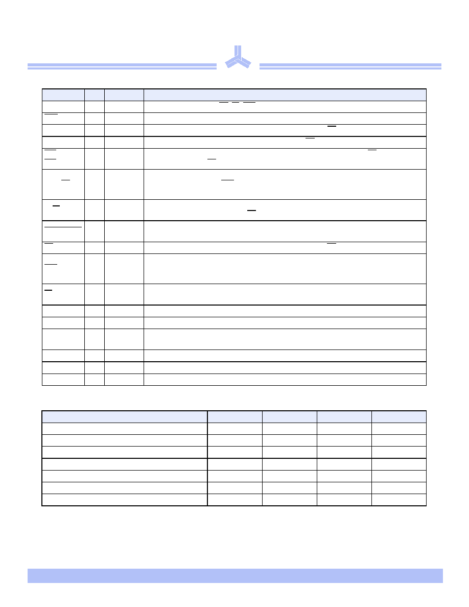
Synchronous truth table
Key: X = don't care, L = low, H = high
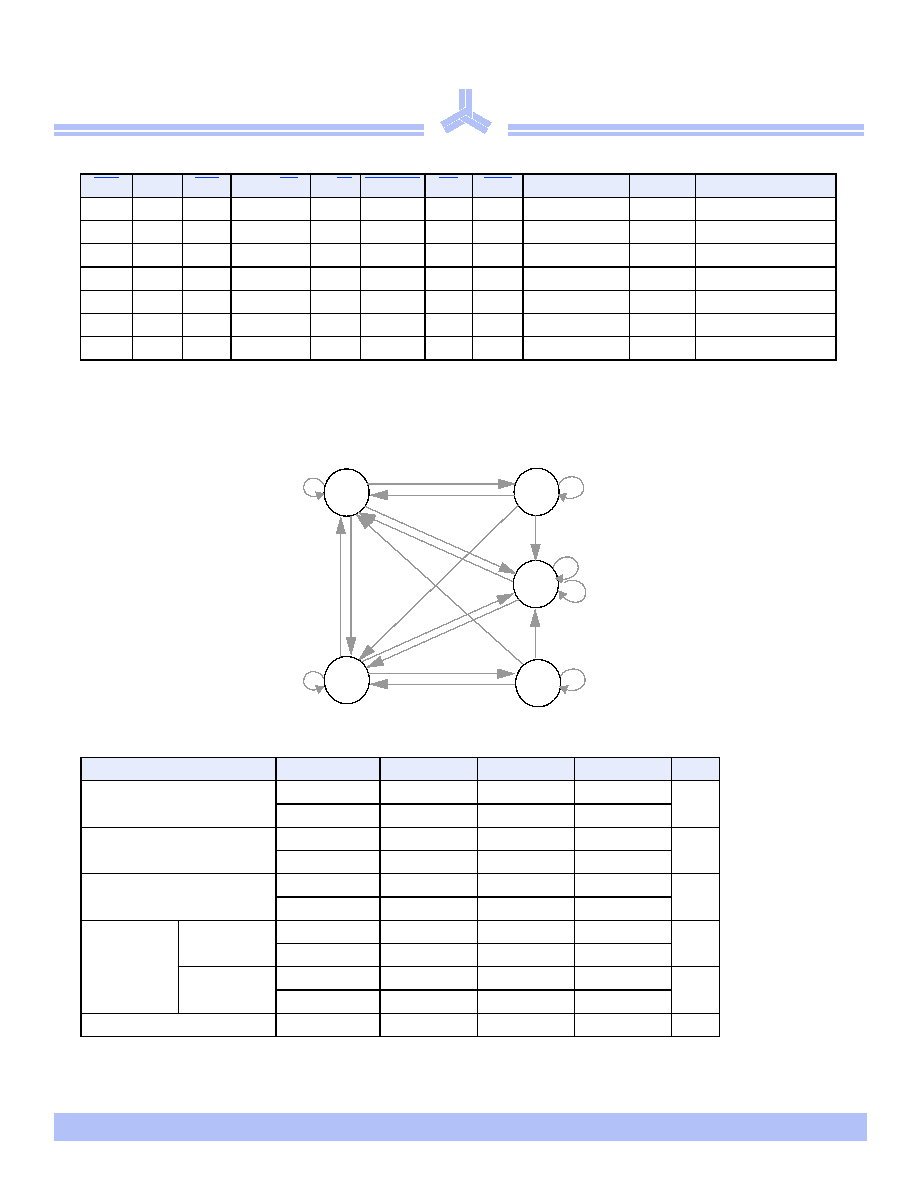
State diagram for NTD SRAM
Recommended operating conditions
CE0
CE1
CE2
ADV/LD
R/W
BW[a,b]
OE
CEN
Address source
CLK
Operation
H
X
X
L
X
X
X
L
NA
L to H
Deselect, high-Z
X
L
X
L
X
X
X
L
NA
L to H
Deselect, high-Z
X
X
H
L
X
X
X
L
NA
L to H
Deselect, high-Z
L
H
L
L
H
X
X
L
External
L to H
Begin read
L
H
L
L
L
L
X
L
External
L to H
Begin write
X
X
X
H
X
X
1
1 Should be low for burst write, unless specific bytes need to be inhibited
X
L
Burst counter
L to H
Burst
2
2 Refer to state diagram below.
X
X
X
X
X
X
X
H
Stall
L to H
Inhibit the CLK
Parameter
Symbol
Min
Nominal
Max
Unit
Supply voltage
V
DD
3.135
3.3
3.465
V
GND
0.0
0.0
0.0
3.3V I/O supply voltage
V
DDQ
2.375
3.3
3.465
V
GND
Q
0.0
0.0
0.0
2.5V I/O supply voltage
V
DDQ
2.35
2.5
2.65
V
GND
Q
0.0
0.0
0.0
Input voltages
1
1 Input voltage ranges apply to 3.3V I/O operation. For 2.5V operation, contact factory for input specifications.
Address and
control pins
V
IH
2.0
V
DD
+ 0.3
V
V
IL
0.5
2
2 V
IL
min = 2.0V for pulse width less than 0.2 x t
RC
.
0.7
I/O pins
V
IH
2.0
V
DDQ
+ 0.3
V
V
IL
-0.5
2
0.7
Ambient operating temperature
T
A
0
70
° C
'VHO
'VHO
5HDG
5HDG
%XUVW
%XUVW
:ULWH
5HDG
:ULWH
%XUVW
5HDG
5HDG
:U
L
W
H
'VHO
5HDG
%XUVW
:ULWH
'VHO
'VH
O
:ULW
H
:
ULWH
%XUVW
'VHO
%XUVW
%XUVW
:ULWH
5HDG
Document Outline