Document Outline
- Features
- . AS7C4098 (5V version)
- . AS7C34098 (3.3V version)
- . Industrial and commercial temperature
- . Organization: 262,144 words ∞ 16 bits
- . Center power and ground pins
- . High speed
- . Low power consumption: ACTIVE
- . Low power consumption: STANDBY
- . Individual byte read/write controls
- . Easy memory expansion with CE, OE inputs
- . TTL- and CMOS-compatible, three-state I/O
- . 44-pin JEDEC standard packages
- . ESD protection ≥ 2000 volts
- . Latch-up current ≥ 100 mA
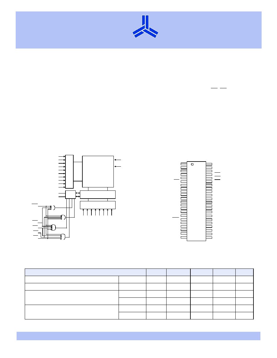
- Logic block diagram
- Pin arrangement for SOJ and TSOP 2
- Functional description
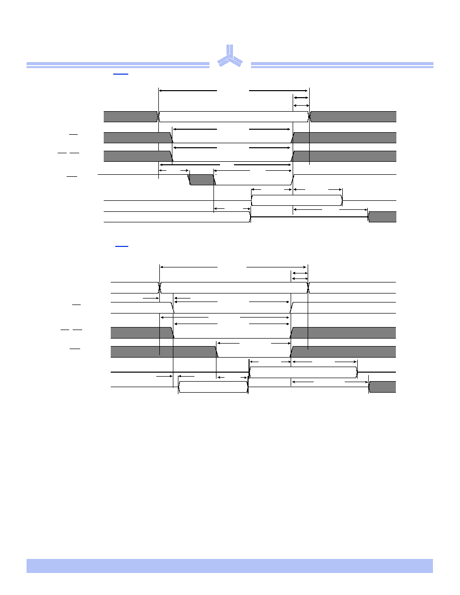
- Key to switching waveforms
- Read waveform 1 (address controlled)6,7,9
- Read waveform 2 (CE, OE, UB, LB controlled)6,8,9
- Write waveform 1(WE controlled)10,11
- Write waveform 2 (CE controlled)10,11
- Write waveform 3 10,11
- AC test conditions
January 2005
Copyright © Alliance Semiconductor. All rights reserved.
Æ
AS7C4098
AS7C34098
5V/3.3V 256K ◊ 16 CMOS SRAM
1/13/05; v.1.9
Alliance Semiconductor
P. 1 of 10
Features
∑ AS7C4098 (5V version)
∑ AS7C34098 (3.3V version)
∑ Industrial and commercial temperature
∑ Organization: 262,144 words ◊ 16 bits
∑ Center power and ground pins
∑ High speed
- 10/12/15/20 ns address access time
- 5/6/7/8 ns output enable access time
∑ Low power consumption: ACTIVE
- 1375 mW (AS7C4098)/max @ 12 ns
- 576 mW (AS7C34098)/max @ 10 ns
∑ Low power consumption: STANDBY
- 110 mW (AS7C4098)/max CMOS
- 72 mW (AS7C34098)/max CMOS
∑ Individual byte read/write controls
∑ Easy memory expansion with CE, OE inputs
∑ TTL- and CMOS-compatible, three-state I/O
∑ 44-pin JEDEC standard packages
- 400-mil SOJ
- TSOP 2
∑ ESD protection
2000 volts
∑ Latch-up current
100 mA
Logic block diagram
1024 ◊ 256 ◊ 16
Array
(4,194,304)
OE
CE
WE
Column decoder
Ro
w De
cod
e
r
A0
A1
A2
A3
A4
A6
A7
A8
V
CC
GND
A12
A5 A9 A10 A1
1
A14 A15 A16 A17
A13
Control circuit
I/O1≠I/O8
I/O9≠I/O16
UB
LB
I/O
buffer
Pin arrangement for SOJ and TSOP 2
5
6
7
8
9
10
11
12
13
14
15
16
17
18
19
20
I/O14
I/O13
GND
V
CC
I/O12
I/O11
I/O10
I/O9
NC
A14
A13
A12
A11
A10
A4
CE
I/O1
I/O2
I/O3
I/O4
V
CC
GND
I/O5
I/O6
I/O7
I/O8
WE
A5
A6
A7
TSOP2
21
22
A8
A9
UB
LB
I/O16
I/O15
2
A1
3
A2
4
A3
1
A0
40
39
38
37
36
35
34
33
32
31
30
29
28
27
26
25
24
23
43
42
41
44
A16
A15
OE
A17
44-pin (400 mil) SOJ
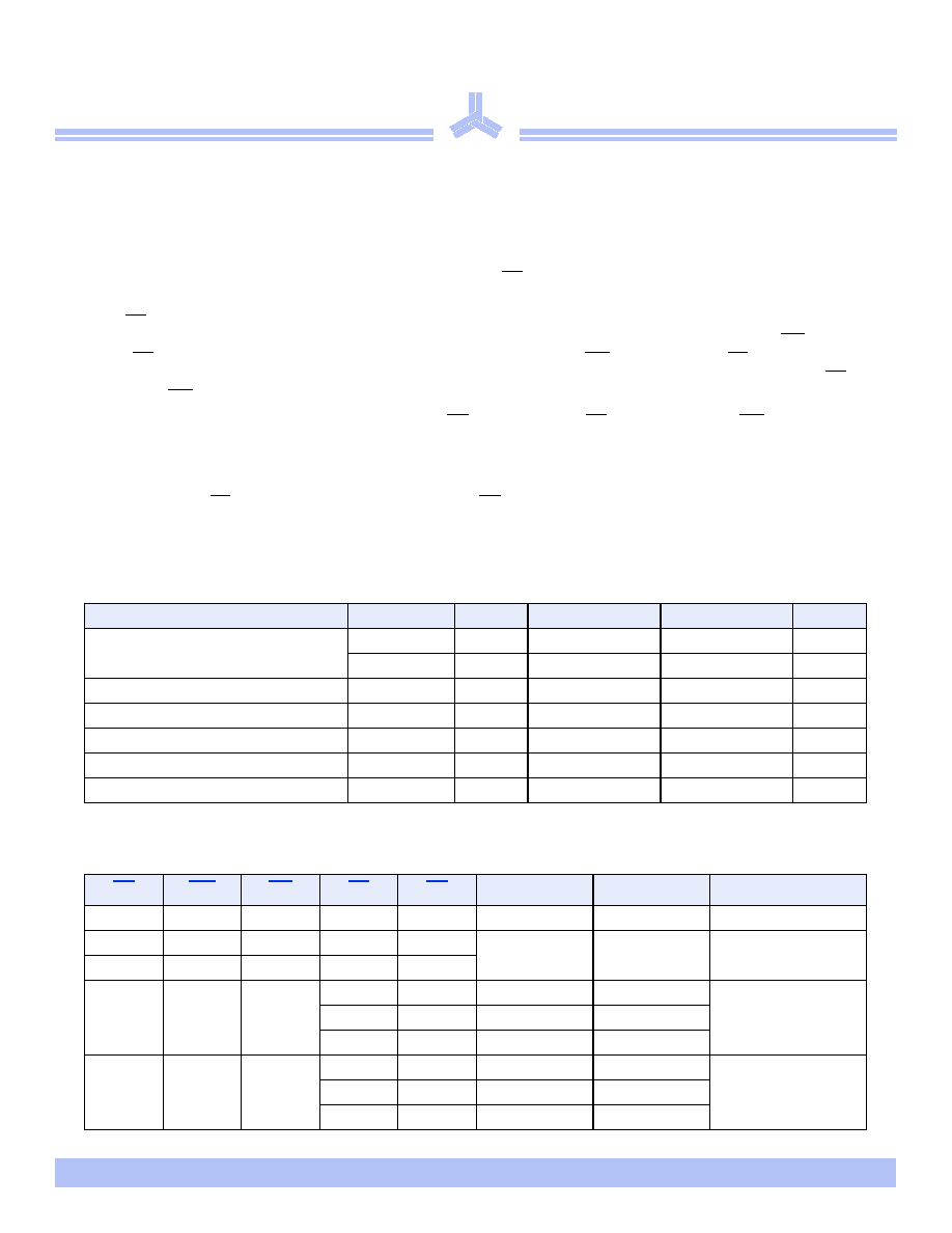
Selection guide
≠10
≠12
≠15
≠20
Unit
Maximum address access time
10
12
15
20
ns
Maximum output enable access time
5
6
7
8
ns
Maximum operating current
AS7C4098
≠
250
220
180
mA
AS7C34098
160
130
110
100
mA
Maximum CMOS standby current
AS7C4098
≠
20
20
20
mA
AS7C34098
20
20
20
20
mA
Æ
AS7C4098
AS7C34098
1/13/05; v.1.9
Alliance Semiconductor
P. 2 of 10
Functional description
The AS7C4098 and AS7C34098 are high-performance CMOS 4,194,304-bit Static Random Access Memory (SRAM) devices
organized as 262,144 words ◊ 16 bits. They are designed for memory applications where fast data access, low power, and
simple interfacing are desired.
Equal address access and cycle times (t
AA
, t
RC
, t
WC
) of 10/12/15/20 ns with output enable access times (t
OE
) of 5/6/7/8 ns are
ideal for high-performance applications. The chip enable input CE permits easy memory expansion with multiple-bank
memory systems.
When CE is High the device enters standby mode. The standard AS7C4098/AS7C34098 is guaranteed not to exceed 110/
72mW power consumption in CMOS standby mode. A write cycle is accomplished by asserting write enable (WE) and chip
enable (CE). Data on the input pins I/O1≠I/O16 is written on the rising edge of WE (write cycle 1) or CE (write cycle 2). To
avoid bus contention, external devices should drive I/O pins only after outputs have been disabled with output enable (OE) or
write enable (WE).
A read cycle is accomplished by asserting output enable (OE) and chip enable (CE), with write enable (WE) High. The chip
drives I/O pins with the data word referenced by the input address. When either chip enable or output enable is inactive, or
write enable is active, output drivers stay in high-impedance mode.
These devices provide multiple center power and ground pins, and separate byte enable controls, allowing individual bytes to
be written and read. LB controls the lower bits, I/O1≠I/O8, and UB controls the higher bits, I/O9≠I/O16.
All chip inputs and outputs are TTL- and CMOS-compatible, and operation is from either a single 5V (AS7C4098) or 3.3V
(AS7C34098) supply. Both devices are available in the JEDEC standard 400-mL, 44-pin SOJ and TSOP 2
packages.
Note: Stresses greater than those listed under Absolute Maximum Ratings may cause permanent damage to the device. This is a stress rating only and
functional operation of the device at these or any other conditions outside those indicated in the operational sections of this specification is not implied.
Exposure to absolute maximum rating conditions for extended periods may affect reliability.
Absolute maximum ratings
Parameter
Device
Symbol
Min
Max
Unit
Voltage on V
CC
relative to GND
AS7C4098
V
t1
≠0.50
+7.0
V
AS7C34098
V
t1
≠0.50
+5.0
V
Voltage on any pin relative to GND
V
t2
≠0.50
V
CC
+0.50
V
Power dissipation
P
D
≠
1.5
W
Storage temperature
T
stg
≠65
+150
∞C
Ambient temperature with V
CC
applied
T
bias
≠55 +125
∞C
DC current into outputs (low)
I
OUT
≠
±20
mA
Truth table
CE
WE
OE
LB
UB
I/O1≠I/O8
I/O9≠I/O16
Mode
H
X
X
X
X
High Z
High Z
Standby (I
SB
, I
SB1
)
L
H
H
X
X
High Z
High Z
Output disable (I
CC
)
L
X
X
H
H
L
H
L
L
H
D
OUT
High Z
Read (I
CC
)
H
L
High Z
D
OUT
L
L
D
OUT
D
OUT
L
L
X
L
H
D
IN
High Z
Write (I
CC
)
H
L
High Z
D
IN
L
L
D
IN
D
IN
Key: X = Don't care, L = Low, H = High.
Æ
AS7C4098
AS7C34098
1/13/05; v.1.9
Alliance Semiconductor
P. 3 of 10
Recommended operating conditions
Parameter
Symbol
Min Typical
Max
Unit
Supply voltage
AS7C4098
V
CC
(12/15/20)
4.5
5.0
5.5
V
AS7C34098
V
CC
(10)
3.15
3.3
3.6
V
AS7C34098
V
CC
(12/15/20)
3.0
3.3
3.6
V
Input voltage
AS7C4098
V
IH
2.2
≠
V
CC
+ 0.5
V
AS7C34098
V
IH
2.0
≠
V
CC
+ 0.5
V
V
IL
1
1 V
IL
min = ≠1.0V for pulse width less than 5ns.
≠0.5
≠
0.8
V
Ambient operating temperature
commercial
T
A
0
≠
70
∞C
industrial
T
A
≠40
≠
85
∞C
DC operating characteristics (over the operating range)
1
Parameter
Symbol
Test conditions
≠10
≠12
≠15
≠20
Unit
Min Max Min Max Min Max Min Max
Input leakage
current
|I
LI
|
V
CC
= Max
V
IN
= GND to V
CC
AS7C4098/
AS7C34098
≠
1
≠
1
≠
1
≠
1
µA
Output leakage
current
|I
LO
|
V
CC
= Max
CE = V
IH
or OE = V
IH
or WE = V
IL
V
I/O
= GND to V
CC
AS7C4098/
AS7C34098
≠
1
≠
1
≠
1
≠
1
µA
Operating
power supply
current
I
CC
V
CC
= Max
Min cycle, 100% duty
CE = V
IL
, I
OUT
= 0mA
AS7C4098
≠
≠
≠
250
≠
220
≠
180 mA
AS7C34098
≠
160
≠
130
≠
110
≠
100 mA
Standby power
supply current
I
SB
V
CC
= Max
CE = V
IH
, f = Max
AS7C4098
≠
≠
≠
60
≠
60
≠
60
mA
AS7C34098
≠
60
≠
60
≠
60
≠
60
mA
I
SB1
V
CC
= Max
CE
V
CC
≠ 0.2V, V
IN
V
CC
≠ 0.2V or V
IN
0.2V, f = 0
AS7C4098
≠
≠
≠
20
≠
20
≠
20
mA
AS7C34098
≠
20
≠
20
≠
20
≠
20
mA
Output voltage
V
OL
I
OL
= 8 mA, V
CC
= Min
AS7C4098/
AS7C34098
≠
0.4
≠
0.4
≠
0.4
≠
0.4
V
V
OH
I
OH
= ≠4 mA, V
CC
= Min
2.4
≠
2.4
≠
2.4
≠
2.4
≠
V
Capacitance (f = 1MHz, T
a
= 25
∞ C, V
CC
= NOMINAL)
2
Parameter
Symbol
Signals
Test conditions
Max
Unit
Input capacitance
C
IN
A, CE, WE, OE, UB, LB
V
IN
= 0V
6
pF
I/O capacitance
C
I/O
I/O
V
IN
= V
OUT
= 0V
8
pF
Æ
AS7C4098
AS7C34098
1/13/05; v.1.9
Alliance Semiconductor
P. 4 of 10
Key to switching waveforms
Read waveform 1 (address controlled)
6,7,9
Read cycle (over the operating range)
3,9
Parameter
Symbol
≠10
≠12
≠15
≠20
Unit Notes
Min
Max
Min Max Min Max Min Max
Read cycle time
t
RC
10
≠
12
≠
15
≠
20
≠
ns
Address access time
t
AA
≠
10
≠
12
≠
15
≠
20
ns
Chip enable (CE) access time
t
ACE
≠
10
≠
12
≠
15
≠
20
ns
Output enable (OE) access time
t
OE
≠
5
≠
6
≠
7
≠
8
ns
Output hold from address change
t
OH
3
≠
3
≠
3
≠
3
≠
ns
5
CE Low to output in low Z
t
CLZ
0
≠
3
≠
0
≠
0
≠
ns
4, 5
CE High to output in higfch Z
t
CHZ
≠
5
≠
6
≠
7
≠
9
ns
4, 5
OE Low to output in low Z
t
OLZ
0
≠
0
≠
0
≠
0
≠
ns
4, 5
OE High to output in high Z
t
OHZ
≠
5
≠
6
≠
7
≠
9
ns
4, 5
LB, UB access time
t
BA
≠
5
≠
6
≠
7
≠
8
ns
LB, UB Low to output in low Z
t
BLZ
0
≠
0
≠
0
≠
0
≠
ns
LB, UB High to output in high Z
t
BHZ
≠
5
≠
6
≠
7
≠
9
ns
Power up time
t
PU
0
≠
0
≠
0
≠
0
≠
ns
5
Power down time
t
PD
≠
10
≠
12
≠
15
≠
20
ns
5
Undefined/don't care
Falling input
Rising input
t
OH
t
AA
t
RC
t
OH
Data
OUT
Address
Data valid
Previous data valid

Æ
AS7C4098
AS7C34098
1/13/05; v.1.9
Alliance Semiconductor
P. 5 of 10
Read waveform 2 (CE, OE, UB, LB controlled)
6,8,9
Write cycle (over the operating range)
11
Parameter
Symbol
≠10
≠12
≠15
≠20
Unit Note
Min
Max
Min
Max
Min
Max
Min
Max
Write cycle time
t
WC
10
≠
12
≠
15
≠
20
≠
ns
Chip enable (CE) to write end
t
CW
7
≠
8
≠
10
≠
12
≠
ns
Address setup to write end
t
AW
7
≠
8
≠
10
≠
12
≠
ns
Address setup time
t
AS
0
≠
0
≠
0
≠
0
≠
ns
Write pulse width (OE = High)
t
WP1
7
≠
8
≠
10
≠
12
≠
ns
Write pulse width (OE = Low)
t
WP2
10
≠
12
≠
15
≠
20
≠
ns
Write recovery time
t
WR
0
≠
0
≠
0
≠
0
≠
ns
Address hold from end of write
t
AH
0
≠
0
≠
0
≠
0
≠
ns
Data valid to write end
t
DW
5
≠
6
7
≠
9
≠
ns
Data hold time
t
DH
0
≠
0
≠
0
≠
0
≠
ns
4, 5
Write enable to output in High-Z
t
WZ
0
5
0
6
0
7
0
9
ns
4, 5
Output active from write end
t
OW
3
≠
3
≠
3
≠
3
≠
ns
4, 5
Byte enable Low to write end
t
BW
7
≠
8
≠
10
≠
12
≠
ns
4, 5
Data valid
t
RC
t
AA
t
BLZ
t
BA
t
OE
t
OLZ
t
OH
t
OHZ
t
CHZ
t
BHZ
t
ACE
t
LZ
Address
OE
CE
LB, UB
Data
OUT
Æ
AS7C4098
AS7C34098
1/13/05; v.1.9
Alliance Semiconductor
P. 6 of 10
Write waveform 1(WE controlled)
10,11
Write waveform 2 (CE controlled)
10,11
Address
CE
LB, UB
WE
Data
IN
Data
OUT
t
WC
t
CW
t
BW
t
AW
t
AS
t
WP
t
DW
t
DH
t
OW
t
WZ
t
AH
Data undefined
High Z
Data valid
t
WR
Address
CE
LB, UB
WE
Data
IN
t
WC
t
CW
t
BW
t
WP
t
DW
t
DH
t
OW
t
WZ
t
AH
Data
OUT
Data undefined
High Z
High Z
t
AS
t
AW
Data valid
t
CLZ
t
WR

Æ
AS7C4098
AS7C34098
1/13/05; v.1.9
Alliance Semiconductor
P. 7 of 10
Write waveform 3
10,11
AC test conditions
Notes
1
During V
CC
power-up, a pull-up resistor to V
CC
on CE is required to meet I
SB
specification.
2
This parameter is sampled, but not 100% tested.
3
For test conditions, see AC Test Conditions, Figures A, B, C.
4
t
CLZ
and t
CHZ
are specified with C
L
= 5pF as in Figure C. Transition is measured ±500mV from steady-state voltage.
5
This parameter is guaranteed, but not tested.
6
WE is High for read cycle.
7
CE and OE are Low for read cycle.
8
Address valid prior to or coincident with CE transition Low.
9
All read cycle timings are referenced from the last valid address to the first transitioning address.
10 CE or WE must be High during address transitions. Either CE or WE asserting high terminates a write cycle.
11 All write cycle timings are referenced from the last valid address to the first transitioning address.
12 Not applicable.
13 C = 30pF, except on High Z and Low Z parameters, where C = 5pF.
Address
CE
LB, UB
WE
Data
IN
t
WC
t
CW
t
BW
t
WP
t
DW
t
DH
t
WZ
t
AH
Data
OUT
Data undefined
High Z
High Z
t
AS
t
AW
Data valid
t
WR
- Output load: see Figure B or Figure C.
- Input pulse level: GND to 3.0V. See Figure A.
- Input rise and fall times: 2 ns. See Figure A.
- Input and output timing reference levels: 1.5V.
10%
90%
10%
90%
GND
+3.0V
2 ns
Figure A: Input pulse
255
C
13
480
D
OUT
GND
+5V
Figure B: 5V Output load
350
C
13
320
D
OUT
GND
+3.3V
Figure C: 3.3V Output load
168
Thevenin equivalent: D
OUT
+1.728V (5V and 3.3V)
Æ
AS7C4098
AS7C34098
1/13/05; v.1.9
Alliance Semiconductor
P. 8 of 10
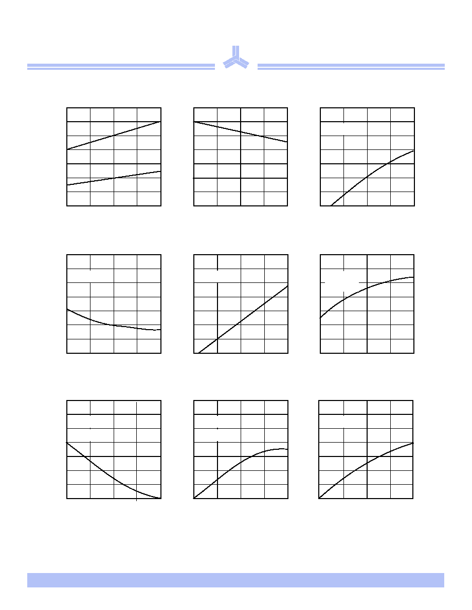
Typical DC and AC characteristics
12
Supply voltage (V)
MIN
MAX
NOMINAL
0.0
0.2
0.6
0.8
0.4
1.0
1.2
1.4
Normali
z
ed I
CC
, I
SB
Normalized supply current ICC, ISB
Ambient temperature (
∞C)
≠55
80
125
35
≠10
0.0
0.2
0.6
0.8
0.4
1.0
1.2
1.4
Normali
z
ed I
CC
, I
SB
Normalized supply current I
CC
, I
SB
vs. ambient temperature T
a
vs. supply voltage VCC
I
CC
I
SB
I
CC
I
SB
Ambient temperature (
∞C)
≠55
80
125
35
≠10
0.2
1
0.04
5
25
625
Normalized ISB1 (log
scale)
Normalized supply current I
SB1
vs. ambient temperature T
a
V
CC
= V
CC
(NOMINAL)
Supply voltage (V)
MIN
MAX
NOMINAL
0.8
0.9
1.1
1.2
1.0
1.3
1.4
1.5
Norm
alized a
cce
ss tim
e
Normalized access time t
AA
Ambient temperature (
∞C)
≠55
80
125
35
≠10
0.8
0.9
1.1
1.2
1.0
1.3
1.4
1.5
Norm
alized a
cce
ss tim
e
Normalized access time t
AA
Cycle frequency (MHz)
0
75
100
50
25
0.0
0.2
0.6
0.8
0.4
1.0
1.2
1.4
Norm
ali
z
ed I
CC
Normalized supply current I
CC
vs. ambient temperature T
a
vs. cycle frequency 1/t
RC
, 1/t
WC
vs. supply voltage V
CC
V
CC
= V
CC
(NOMINAL)
T
a
= 25
∞ C
V
CC
= V
CC
(NOMINAL)
T
a
= 25
∞ C
Output voltage (V)
V
CC
0
20
60
80
40
100
120
140
Output source curr
ent
(mA)
Output source current I
OH
Output voltage (V)
V
CC
Output sink cur
r
ent (mA)
Output sink current I
OL
vs. output voltage V
OL
vs. output voltage V
OH
0
20
60
80
40
100
120
140
V
CC
= V
CC
(NOMINAL)PL
T
a
= 25
∞ C
V
CC
= V
CC
(NOMINAL)
T
a
= 25
∞ C
Capacitance (pF)
0
750
1000
500
250
0
5
15
20
10
25
30
35
Change in t
AA
(ns)
Typical access time change
t
AA
vs. output capacitive loading
V
CC
= V
CC
(NOMINAL)
0
0
Æ
AS7C4098
AS7C34098
1/13/05; v.1.9
Alliance Semiconductor
P. 9 of 10
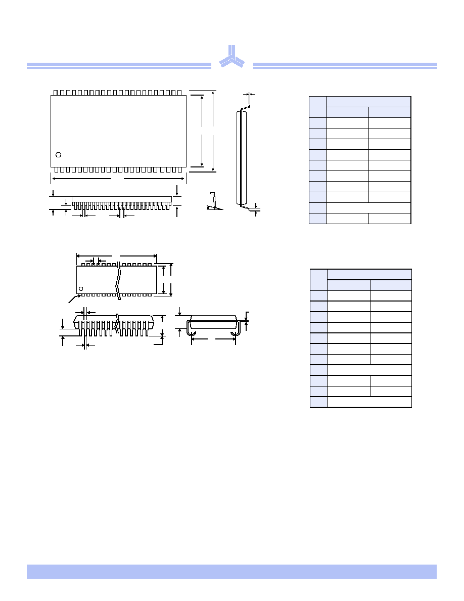
Package dimensions
44-pin TSOP 2
Min (mm)
Max (mm)
A
1.2
A
1
0.05
0.15
A
2
0.95
1.05
b
0.30
0.45
c
0.12
0.21
d
18.31
18.52
e
10.06
10.26
H
e
11.68
11.94
E
0.80 (typical)
l
0.40
0.60
d
H
e
1 2 3 4 5 6 7 8 9 1011121314
44 43424140393837363534333231
1516
3029
1718 1920
272625
c
l
A
1
A
2
E
44-pin TSOP 2
0≠5
∞
21
24
22
23
e
A
b
44-pin SOJ 400 mils
Min(mils)
Max(mils)
A
0.128
0.148
A1
0.025
-
A2
0.105
0.115
B
0.026
0.032
b
0.015
0.020
c
0.007
0.013
D
1.120
1.130
E
0.370 NOM
E1
0.395
0.405
E2
0.435
0.445
e
0.050 NOM
Seating
Plane
44-pin SOJ
28
Pin 1
D
e
E2
E1
A1
b
B
A
A2
E
c
AS7C4098
AS7C34098
© Copyright Alliance Semiconductor Corporation. All rights reserved. Our three-point logo, our name and Intelliwatt are trademarks or registered trademarks of Alliance. All other brand and product names may be the trade-
marks of their respective companies. Alliance reserves the right to make changes to this document and its products at any time without notice. Alliance assumes no responsibility for any errors that may appear in this document.
The data contained herein represents Alliance's best data and/or estimates at the time of issuance. Alliance reserves the right to change or correct this data at any time, without notice. If the product described herein is under
development, significant changes to these specifications are possible. The information in this product data sheet is intended to be general descriptive information for potential customers and users, and is not intended to operate
as, or provide, any guarantee or warrantee to any user or customer. Alliance does not assume any responsibility or liability arising out of the application or use of any product described herein, and disclaims any express or
implied warranties related to the sale and/or use of Alliance products including liability or warranties related to fitness for a particular purpose, merchantability, or infringement of any intellectual property rights, except as
express agreed to in Alliance's Terms and Conditions of Sale (which are available from Alliance). All sales of Alliance products are made exclusively according to Alliance's Terms and Conditions of Sale. The purchase of
products from Alliance does not convey a license under any patent rights, copyrights, mask works rights, trademarks, or any other intellectual property rights of Alliance or third parties. Alliance does not authorize its products
for use as critical components in life-supporting systems where a malfunction or failure may reasonably be expected to result in significant injury to the user, and the inclusion of Alliance products in such life-supporting sys-
tems implies that the manufacturer assumes all risk of such use and agrees to indemnify Alliance against all claims arising from such use.
1/13/05; v.1.9
Alliance Semiconductor
P. 10 of 10
Æ
Note:
Add suffix "N" to the above part number for lead free devices, Ex. AS7C4098-12JCN
Ordering Codes
Package
Version
10 ns
12 ns
15 ns
20 ns
SOJ
5V commercial
NA
AS7C4098-12JC
AS7C4098-15JC
AS7C4098-20JC
5V industrial
NA
AS7C4098-12JI
AS7C4098-15JI
AS7C4098-20JI
3.3V commercial
AS7C34098-10JC
AS7C34098-12JC
AS7C34098-15JC
AS7C34098-20JC
3.3V industrial
NA
AS7C34098-12JI
AS7C34098-15JI
AS7C34098-20JI
TSOP 2
5V commercial
NA
AS7C4098-12TC
AS7C4098-15TC
AS7C4098-20TC
5V industrial
NA
AS7C4098-12TI
AS7C4098-15TI
AS7C4098-20TI
3.3V commercial AS7C34098-10TC
AS7C34098-12TC
AS7C34098-15TC
AS7C34098-20TC
3.3V industrial
NA
AS7C34098-12TI
AS7C34098-15TI
AS7C34098-20TI
Part numbering system
AS7C
X
4098
≠XX
J or T
X
N
SRAM prefix
Voltage:
Blank: 5V CMOS
3: 3.3V CMOS
Device
number
Access
time
Packages:
J: SOJ 400 mil
T: TSOP 2
Temperature ranges:
C: Commercial, 0∞C to 70∞C
I: Industrial, ≠40∞C to 85∞C
Lead free device