Äîêóìåíòàöèÿ è îïèñàíèÿ www.docs.chipfind.ru
June 2005
ASM2P2304NZ
rev 0.4
Alliance Semiconductor
2575, Augustine Drive
·
Santa Clara, CA
·
Tel: 408.855.4900
·
Fax: 408.855.4999
·
www.alsc.com
Notice: The information in this document is subject to change without notice.
Four Output PCI-X and General Purpose Buffer
Features
One input to four Output Buffer/Driver
General-purpose or PCI-X clock buffer
Buffers all frequencies from DC to 140 MHz
Output-to-output skew less than 100 pS
Space-saving 8-pin TSSOP Package
3.3V operation
Functional Description
The ASM2P2304NZ is a low-cost buffer designed to
distribute high-speed clocks for PCI-X and other
applications. The device operates at 3.3V and outputs can
run up to 140 MHz.
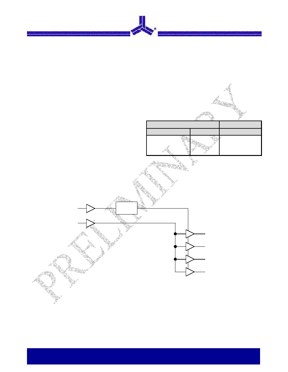
Table 1. Function Table.
Inputs
Outputs
BUF_IN
OE
Output [1:4]
L
H
L
H
L
L
H
H
L
L
L
H
Block Diagram
Logic
Control
OUTPUT 1
OUTPUT 2
OUTPUT 3
OUTPUT 4
OE
BUF_ IN
June 2005
ASM2P2304NZ
rev 0.4
Four Output PCI-X and General Purpose Buffer
2 of 8
Notice: The information in this document is subject to change without notice.
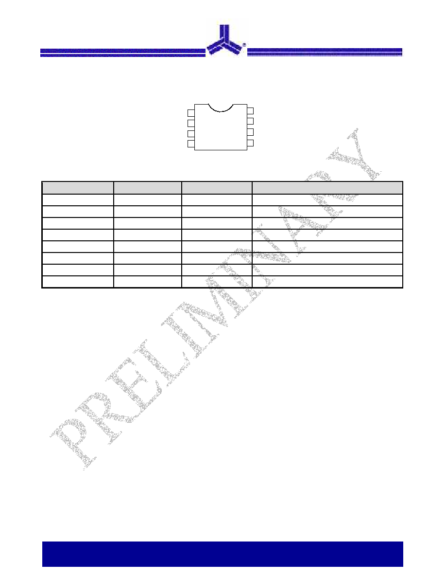
Pin Configuration
Pin Description
Pin #
Pin Name
Type
Description
1
BUF_IN
I
Input clock. 5V Tolerant Input
2
OE
I
Input pin for Output Enable, active HIGH.
3
Output 1
O
Output 1
4
GND P
Ground
5
Output 2
O
Output 2
6
V
DD
P
3.3V Voltage Supply
7
Output 3
O
Output 3
8
Output 4
O
Output 4
OUTPUT 1
1
2
3
4
8
7
6
5
BUF_IN
OE
OUTPUT 4
OUTPUT 3
OUTPUT 2
GND
V
DD
8 TSSOP
Top V iew
ASM2P2304NZ
June 2005
ASM2P2304NZ
rev 0.4
Four Output PCI-X and General Purpose Buffer
3 of 8
Notice: The information in this document is subject to change without notice.
Absolute Maximum Ratings
Parameter
Min
Max
Unit
Supply Voltage to Ground Potential
-0.5
7
V
DC Input Voltage (Except REF)
-0.5
V
DD
+ 0.5
V
DC Input Voltage (REF)
-0.5
7
V
Storage Temperature
-65
+150
°C
Max. Soldering Temperature (10 sec)
260
°C
Junction Temperature
150
°C
Static Discharge Voltage
(As per JEDEC STD22- A114-B)
2000
V
Note: These are stress ratings only and functional usage is not implied. Exposure to absolute maximum ratings for prolonged periods can affect device
reliability.
Operating Conditions
Parameter
Description
Min
Max
Unit
V
DD
Supply
Voltage
3.0
3.6
V
T
A
Operating Temperature (Ambient Temperature)
-40
85
°C
C
L
Load Capacitance
-
25
pF
C
IN
Input
Capacitance
-
7
pF
BUF_IN,
OUTPUT [1:4]
Operating Frequency
DC
140
MHz
t
PU
Power-up time for all V
DD
's to reach minimum specified
Voltage (Power ramps must be monotonic)
0.05 50 mS
June 2005
ASM2P2304NZ
rev 0.4
Four Output PCI-X and General Purpose Buffer
4 of 8
Notice: The information in this document is subject to change without notice.
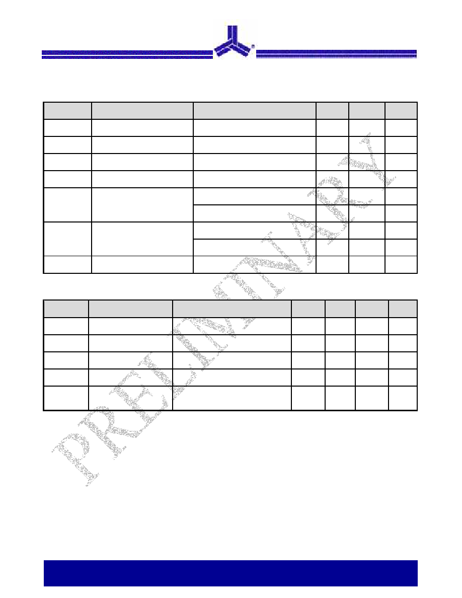
Electrical Characteristics
Parameter
Description
Test Conditions
Min
Max
Unit
V
IL
Input LOW Voltage
1
-
0.8 V
V
IH
Input HIGH Voltage
1
2.0 - V
I
IL
Input
LOW
Current
V
IN
= 0V
5
5
KA
I
IH
Input HIGH Current
V
IN
= V
DD
5
5
KA
I
OL
= 24 mA
-
0.8
V
V
OL
Output
LOW
Voltage
2
I
OL
= 12 mA
-
0.55
V
I
OH
= 24 mA
2.0
-
V
V
OH
Output HIGH Voltage
2
I
OH
= 12 mA
2.4
-
V
I
DD
Supply Current
Unloaded outputs at 66.66 MHz
-
25
mA
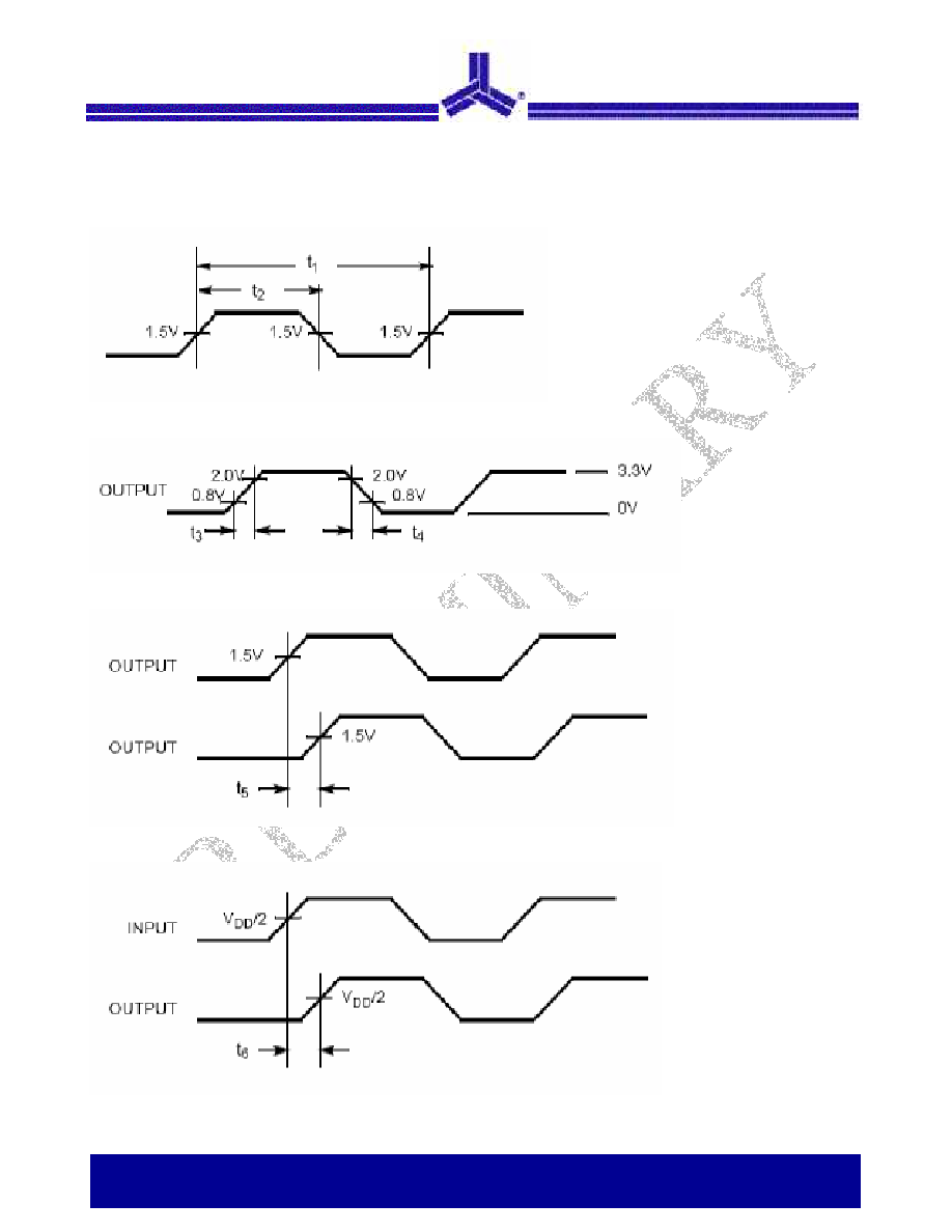
Switching Characteristics for Commercial and Industrial Temperature Devices
3
Parameter
Name
Description
Min
Typ
Max
Unit
t
D
Duty Cycle
2
= t
2
÷t
1
Measured at 1.5V
40.0
50.0
60.0
%
t
3
Rise Time
2
Measured between 0.8V and 2.0V
-
-
1.50
nS
t
4
Fall Time
2
Measured between 0.8V and 2.0V
-
-
1.50
nS
t
5
Output to Output Skew
2
All outputs equally loaded
-
-
200
pS
t
6
Propagation Delay,
BUF_IN Rising Edge to
OUTPUT Rising Edge
2
Measured at V
DD
/2
2.5 3.5 5 nS
Note:
1. BUF_IN input has a threshold voltage of V
DD
/2.
2. Parameter is guaranteed by design and characterization. It is not 100% tested in production.
3. All parameters specified with loaded outputs.
June 2005
ASM2P2304NZ
rev 0.4
Four Output PCI-X and General Purpose Buffer
5 of 8
Notice: The information in this document is subject to change without notice.
Switching Waveforms
Duty Cycle Timing
All Outputs Rise/Fall Time
Output-Output Skew
Input-Output Propagation Delay