 | –≠–ª–µ–∫—Ç—Ä–æ–Ω–Ω—ã–π –∫–æ–º–ø–æ–Ω–µ–Ω—Ç: L2042A | –°–∫–∞—á–∞—Ç—å:  PDF PDF  ZIP ZIP |

October 2003
L2042A
rev 1.0
Alliance Semiconductor
2575, Augustine Drive
∑∑
Santa Clara, CA
∑∑
Tel: 408.855.4900
∑∑
Fax: 408.855.4999
∑∑
www.alsc.com
2.5V LCD Panel Reduction IC
Features
ß
FCC approved method of EMI attenuation.
ß
Provides up to 15dB of EMI suppression.
ß
Generates a low EMI spread spectrum clock of the
input frequency.
ß
Input frequency range: 30MHz to 75 MHz.
ß
Optimized for 32.5MHz, 54MHz, and 65MHz.
ß
Internal loop filter minimizes external components
and board space.
ß
Selectable spread deviation.
ß
SSON# control pin for spread spectrum enable
and disable options.
ß
Low cycle-to-cycle jitter.
ß
2.5V or 3.3V operating voltage range.
ß
TTL or CMOS compatible outputs.
ß
Ultra-low power CMOS design.
ß
Supports most mobile graphic accelerator and
LCD timing controller specifications.
ß
Available in 8-pin SOIC and TSSOP.
Product Description
The L2042A is a versatile spread spectrum frequency
modulator designed specifically for digital falt panel
applications. The L2042A reduces electromagnetic
interference (EMI) at the clock source, allowing system
wide reduction of EMI of down stream clock and data
dependent signals. The L2042A allows significant system
cost savings by reducing the number of circuit board
layers ferrite beads, shielding and other passive
components that are traditionally required to pass EMI
regulations.
The L2042A uses the most efficient and optimized
modulation profile approved by the FCC and is
implemented in a proprietary all digital method.
The L2042A modulates the output of a single PLL in
order to "spread" the bandwidth of a synthesized clock,
and more importantly, decreases the peak amplitudes of
its harmonics. This results in significantly lower system
EMI compared to the typical narrow band signal produced
by oscillators and most frequency generators. Lowering
EMI by increasing a signal's bandwidth is called `spread
spectrum clock generation'.
Applications
The L2042A is targeted towards digital flat panel
applications for Notebook PCs, Palm -size PCs, office
automation equipment, and LCD monitors.
Block Diagram
VSS
CLKIN
Frequency
Divider
Feedback
Divider
Modulation
Phase
Detector
Loop
Filter
VCO
Output
Divider
MODOUT
PLL
VDD
SSON#
DIV2
SR0
CP0
CP1
October 2003
L2042A
rev 1.0
2.5V LCD Panel EMI Reduction IC
2 of 10
1
2
3
4
5
6
7
8
L2042A
XIN /CLK
CP0
CP1
VSS
SSON#
ModOUT
SR0
VDD
Pin Configuration
Pin Description
Pin#
Pin Name
Type
Description
1
CLKIN
I
External reference frequency input. Connect to an externally generated
reference signal.
2
CP0
I
Digital logic input used to select charge pump current. Refer Modulation
Selection Table. This pin has an internal pull-up resistor.
3
CP1
I
Digital logic input used to select charge pump current. Refer Modulation
Selection Table. This pin has an internal pull-up resistor.
4
VSS
P
Ground to entire chip. Connect to system ground.
6
SSON#
I
Digital logic input used to enable Spread Spectrum function (Active LOW).
Spread Spectrum function enabled when LOW, disabled when HIGH. This
pin has an internal pull-low resistor.
7
ModOUT
O
Spread spectrum clock output.
5
SR0
I
Digital logic input used to select Spreading Range Refer Modulation
Selection Table. This pin has an internal pull-up resistor.
8
VDD
P
Power supply for the entire chip (+2.5V or 3.3V)
Modulation Selection Table
Spreading Range (
±
±
%)
CP0
CP1
SR0
32.5MHz
54MHz
65MHz
70MHz
Modulation Rate
0
0
0
0.49
0.92
0.88
0.87
0
0
1
1.71
1.48
1.37
1.32
0
1
0
1.2
0.92
0.88
0.84
0
1
1
1.69
1.48
1.37
1.33
1
0
0
1.09
0.71
0.58
0.42
1
0
1
1.68
1.14
0.9
0.73
1
1
0
0.8
0.4
0.3
0.25
1
1
1
1.29
0.62
0.48
0.37
(F
IN
/40) * 62.49 KHz
October 2003
L2042A
rev 1.0
2.5V LCD Panel EMI Reduction IC
3 of 10
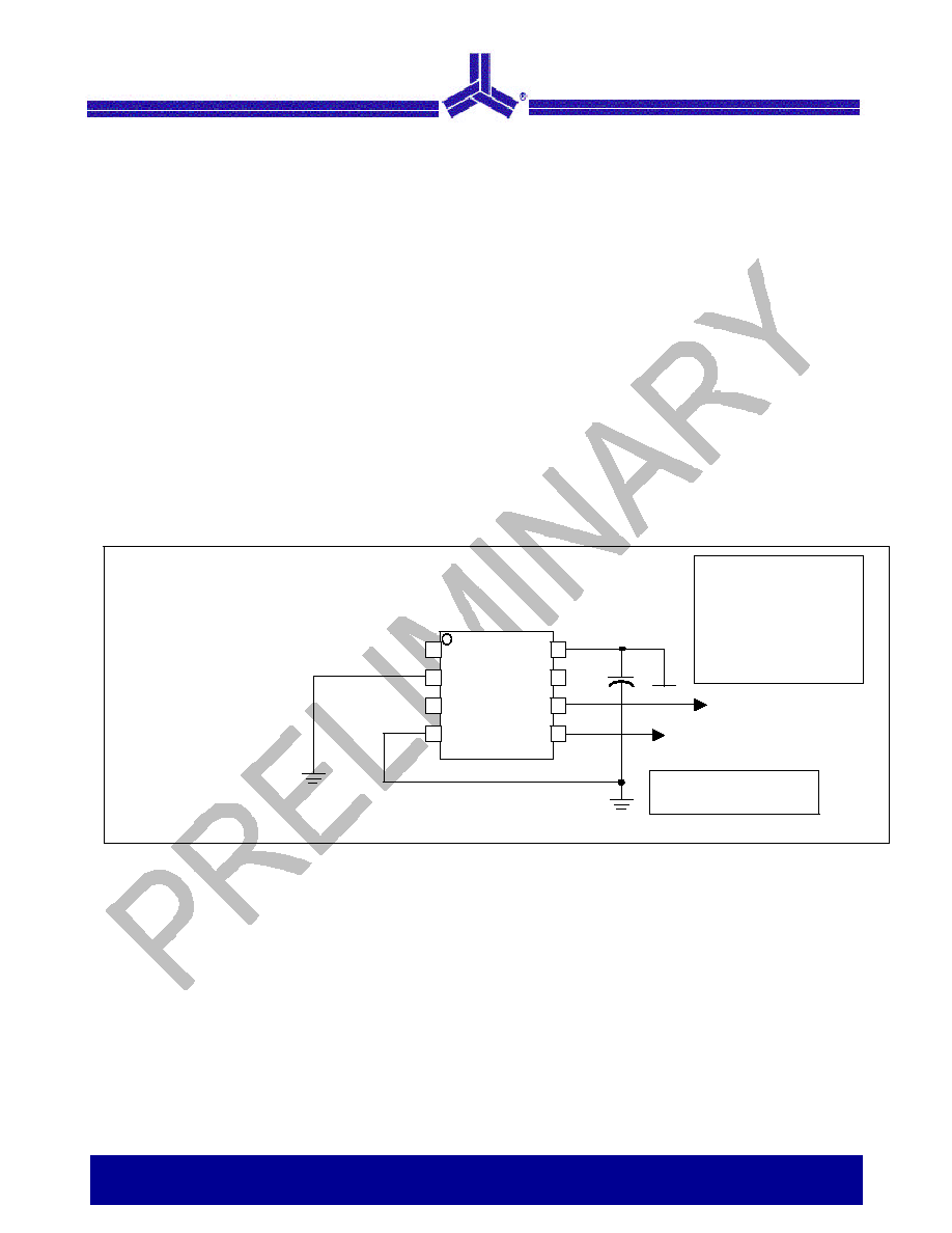
1
2
3
4
CLKIN
CP0
CP1
VSS
SR0
5
6
7
8
SSON#
ModOUT
VDD
L2042A
Spread Spectrum
The Modulation Selection Table illustrates the possible spread spectrum options. The optimal setting should
minimize system EMI to the fullest without affecting system performance. The spreading is described as a
percentage deviation of the center frequency (Note: The center frequency is the frequency of the external
reference input on CLKIN, Pin1).
Example:
The L2042A is designed for high-resolution flat panel applications and is able to support panel frequencies from
30 to 75 MHz. For a 65MHz pixel clock frequency, a spreading selection of CP0=0 and CP1=1 and SR0=1 gives
a percentage deviation of TBD%. Refer Modulation Selection Table. This results in frequency on ModOUT being
swept from TBD to TBD MHz. This particular example (See figure below) given here is a common EMI reduction
method for notebook LCD panel and has already been implemented by most of the leading OEM and mobile
graphic accelerator manufacturers.
65 MHz from Graphics Accelerator
Modulated 65MHz signal
with 1.5% deviation and
modulation rate of
50.77KHz. This signal is
connected back to the
spread spectrum input pin
(SSIN) of the graphics
accelerator
VDD
0.1µF
Digital control for SS
Enable or Disable
October 2003
L2042A
rev 1.0
2.5V LCD Panel EMI Reduction IC
4 of 10
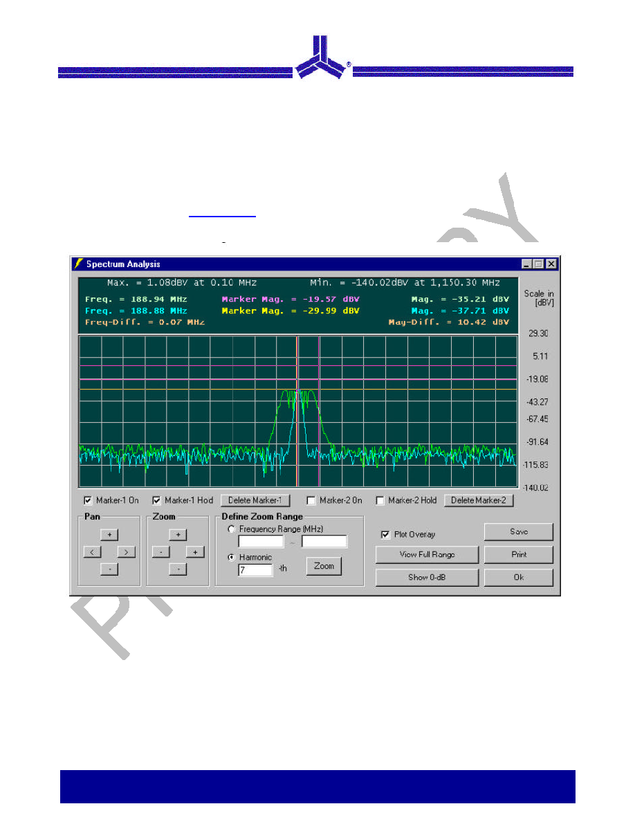
EMC Software Simulation
By using Alliance's proprietary EMC simulation software ≠ EMI-LatorÆ, radiated system level EMI analysis can
be made easier, allowing quantitative measure on the benefits of Alliance's EMI reduction products. The
simulation engine of this EMC software has already been characterized to correlate with the electrical
characteristics of Alliance EMI reduction ICs. The figure below is an illustration of this simulation result.
Please visit our website at
www.alsc.com
for information on how to obtain a free copy and demonstration of
EMI-Lator Æ.
Simulation results From EMI-LatorÆ
October 2003
L2042A
rev 1.0
2.5V LCD Panel EMI Reduction IC
5 of 10
Absolute Maximum Ratings
Symbol
Parameter
Rating
Unit
V
DD
, V
IN
Voltage on any pin with respect to GND
-0.5 to + 7.0
V
T
STG
Storage temperature
-65 to +125
∞C
T
A
Operating temperature
0 to 70
∞C
Note: These are stress ratings only and functional operation is not implied. Exposure to absolute maximum
ratings for extended periods may affect device reliability.
DC Electrical Characteristics
Symbol
Parameter
Min
Typ
Max
Unit
V
IL
Input low voltage
GND ≠ 0.3
-
0.8
V
V
IH
Input high voltage
2.0
-
V
DD
+ 0.3
V
I
IL
Input low current (pull-up resistors on inputs SR0, SR1,
CP0 and CP1)
-
-
-35
µA
I
IH
Input high current (pull-down resistor on input SSON#)
-
-
35
µA
V
OL
Output low voltage (V
DD
= 3.3V, I
OL
= 20mA)
-
-
0.4
V
V
OH
Output high voltage (V
DD
= 3.3V, I
OH
= 20mA)
2.5
-
-
V
I
CC
Dynamic supply current normal mode (2.5V, and 15pF
loading)
TBD @
30MHz
-
TBD
@70MHz
mA
I
DD
Static supply current standby mode
-
0.6
-
mA
V
DD
Operating voltage
2.25
2.85
3.7
V
t
ON
Power up time (first locked clock cycle after power up)
-
0.18
-
mS
Z
OUT
Clock output impedance
-
50
-