
Alliance Semiconductor
Production
March 2003
P1818/19/20/21/22
Low Power Mobile VGA EMI Reduction IC
2575 Augustine Drive ∑ Santa Clara, CA 95054 ∑ Tel: 408.855.4900 ∑ Fax: 408.855.4999 ∑ www.alsc.com
Æ
Notice: The information in this document is subject to change without notice.
Features
∑
FCC approved method of EMI attenuation
∑
Provides up to 15 dB EMI reduction
∑
Generates a low EMI spread spectrum clock and a
non-spread reference clock of the input frequency
∑
Optimized for frequency range from 10 MHz to 160
MHz
P1818: 10 to 20 MHz
P1819: 20 to 40 MHz
P1820: 40 to 80 MHz
P1821: 10 to 40 MHz
P1822: 80 to 160 MHz
∑
Internal loop filter minimizes external components
and board space
∑
Selectable spread options: Down Spread and Cen-
ter Spread
∑
Low inherent cycle-to-cycle jitter
∑
Eight spread % selections: +/-0.625% to ≠3.5%
∑
3.3V operating voltage
∑
CMOS/TTL compatible inputs and outputs
∑
Low power CMOS design
∑
Supports notebook VGA and other LCD timing
controller applications
∑
Power down function for mobile application
∑
Products are available for industrial temperature
range.
∑
Available in 8-pin SOIC and TSSOP
Product Description
The P18xx is a versatile spread spectrum frequency
modulator designed specifically for a wide range of input
clock frequencies from 10 to 160 MHz (see Input Fre-
quency and Modulation Rate Selections). The P18xx
can generate an EMI reduced clock from crystal,
ceramic resonator, or system clock. The P18xx-A to
P18xx-H offer various combinations of spread options
and percentage deviations (see Spread Deviation Selec-
tions). These combinations include Down Spread,
Center Spread and percentage deviation range from
±0.625% to -3.50%.
The P18xx reduces electromagnetic interference (EMI)
at the clock source, allowing a system wide EMI
reduction for all the down stream clocks and data
dependent signals. The P18xx allows significant system
cost savings by reducing the number of circuit board
layers, ferrite beads, shielding, and other passive
components that are traditionally required to pass EMI
regulations.
The P18xx modulates the output of a single PLL in
order to "spread" the bandwidth of a synthesized clock,
thereby decreasing the peak amplitudes of its
harmonics. This results in significantly lower system
EMI compared to the typical narrow band signal
produced by oscillators and most clock generators.
Lowering EMI by increasing a signal's bandwidth is
called "spread spectrum clock generation".
The P18xx uses the most efficient and optimized
modulation profile approved by the FCC and is
implemented by using a proprietary all-digital method.
Applications
The P18xx is targeted toward EMI management for
memory and LVDS interfaces in mobile graphic
chipsets and high-speed digital applications such as
PC peripheral devices, consumer electronics, and
embedded controller systems.
Æ
Low Power Mobile VGA EMI Reduction IC
2 of 8
March 2003
P1818/19/20/21/22
Notice: The information in this document is subject to change without notice.
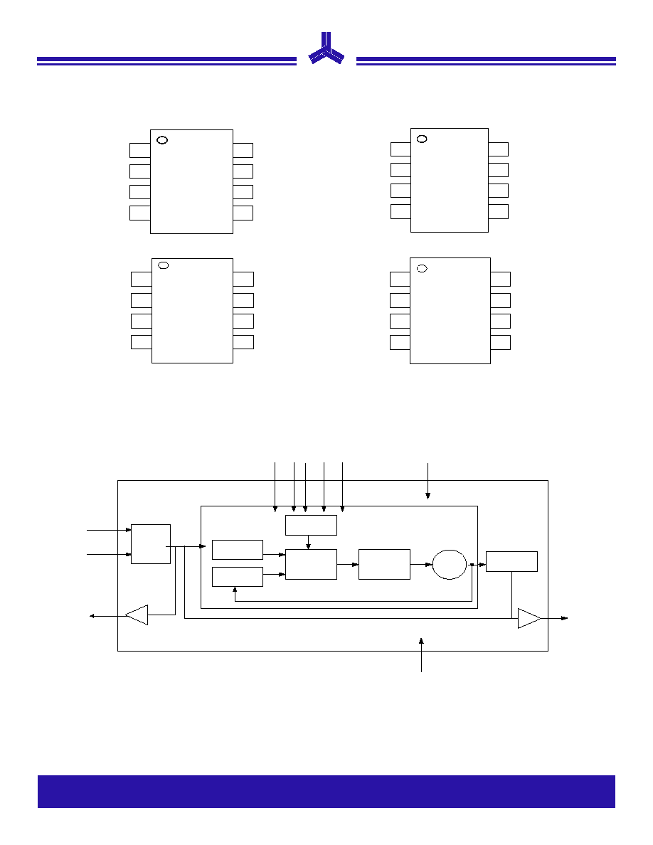
Pin Diagrams
Block Diagram
P 1 8 1 8 A / B / C / D
P 1 8 1 9 A / B / C / D
P 1 8 2 0 A / B / C / D
1
8
6
4
3
2
7
5
X I N
V S S
S R S
M o d O u t
X O U T
V D D
P D #
R E F
P 1 8 2 1 A /B /C /D
1
8
6
4
3
2
7
5
X IN
V S S
S R S
M o d O u t
X O U T
V D D
F R S
R E F
1
8
6
4
3
2
7
5
X I N
V S S
D _ C
M o d O u t
X O U T
V D D
P D #
R E F
P 1 8 1 8 E / F / G / H
P 1 8 1 9 E / F / G / H
P 1 8 2 0 E / F / G / H
P 1 8 2 2 A
1
8
6
4
3
2
7
5
X IN
V S S
S R S
M o d O u t
M R S
V D D
S S O N #
S R 0
P1818/19/20/21/22 Block Diagram
Output
Divider
XIN
VSS
ModOUT
XOUT
Crystal
Oscillator
Modulation
Phase
Detector
Frequency
Divider
Feedback
Divider
Loop
Filter
VCO
PLL
D_C PD# MRS FRS SRS
VDD
REF
Æ
Low Power Mobile VGA EMI Reduction IC
3 of 8
March 2003
P1818/19/20/21/22
Notice: The information in this document is subject to change without notice.
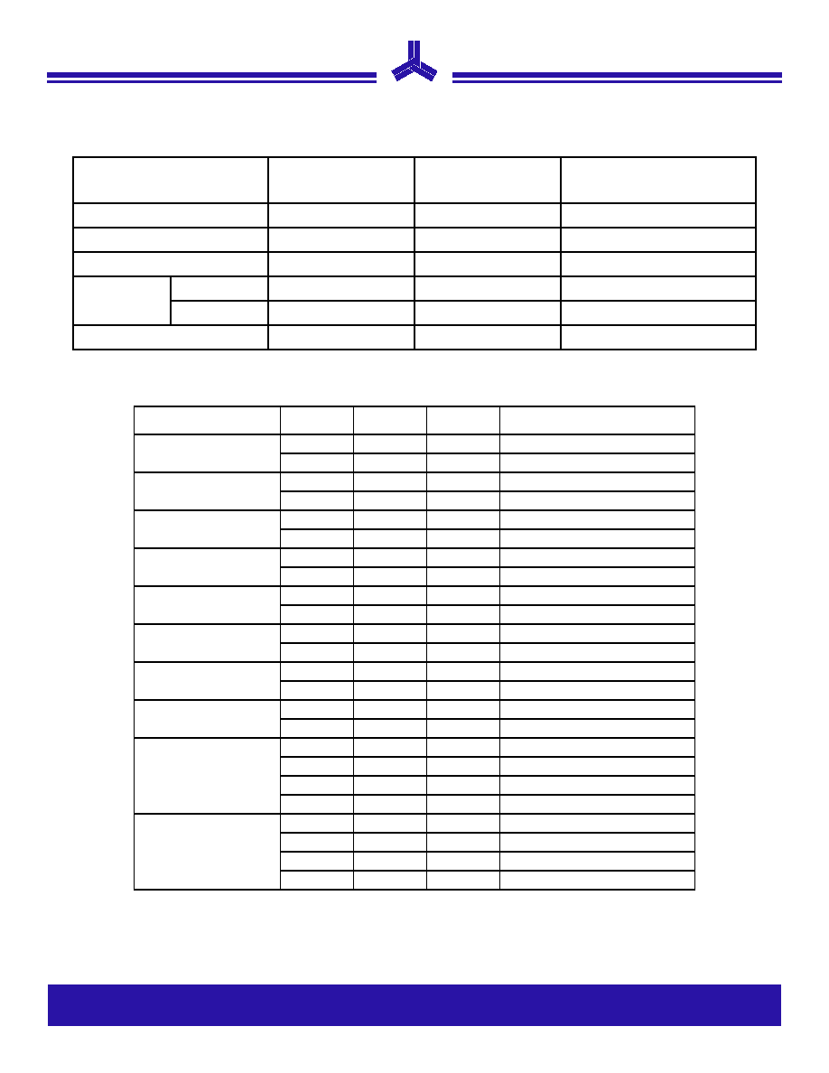
Input Frequency and Modulation Rate
Spread Deviation Selections
Part number
Input
frequency range
Output
frequency range
Modulation rate
P1818
10 MHz to 20 MHz
10 MHz to 20 MHz
Input frequency / 256
P1819
20 MHz to 40 MHz
20 MHz to 40 MHz
Input frequency / 512
P1820
40 MHz to 80 MHz
40 MHz to 80 MHz
Input frequency / 2048
P1821
FRS=0
10 MHz to 20 MHz
10 MHz to 20 MHz
Input frequency / 256
FRS=1
20 MHz to 40 MHz
20 MHz to 40 MHz
Input frequency / 512
P1822
80 MHz to 160 MHz
80 MHz to 160 MHz
Input frequency / 3584
Part number
1
1. A through H represents various combinations of spread deviations, options, and modulation rates.
SRS
SR0
D_C
Spread deviation
P1818
2
/19/20/21A
2. Refer to Frequency vs. Deviation (P1818A and P1818H).
0
N/A
N/A
-2.50% (Down)
1
-3.50% (Down)
P1818/19/20/21B
0
N/A
N/A
-1.25% (Down)
1
-1.75% (Down)
P1818/19/20/21C
0
N/A
N/A
+/-1.25% (Center)
1
+/-1.75% (Center)
P1818/19/20/21D
0
N/A
N/A
+/-0.625% (Center)
1
+/-0.875% (Center)
P1818/19/20E
N/A
N/A
0
-1.25% (Down)
1
+/-0.625% (Center)
P1818/19/20F
N/A
N/A
0
-2.5% (Down)
1
+/-1.25% (Center)
P1818/19/20G
N/A
N/A
0
-1.75% (Down)
1
+/-0.875% (Center)
P1818
2
/19/20H
N/A
N/A
0
-3.5% (Down)
1
+/-1.75% (Center)
P1822A
0
0
N/A
-1.25% (Down)
0
1
-2.50% (Down)
1
0
-1.75% (Down)
1
1
-3.50% (Down)
P1822B
0
0
N/A
+/-0.625% (Center)
0
1
+/-1.25% (Center)
1
0
+/-0.875% (Center)
1
1
+/-1.75% (Center)
Æ
Low Power Mobile VGA EMI Reduction IC
4 of 8
March 2003
P1818/19/20/21/22
Notice: The information in this document is subject to change without notice.
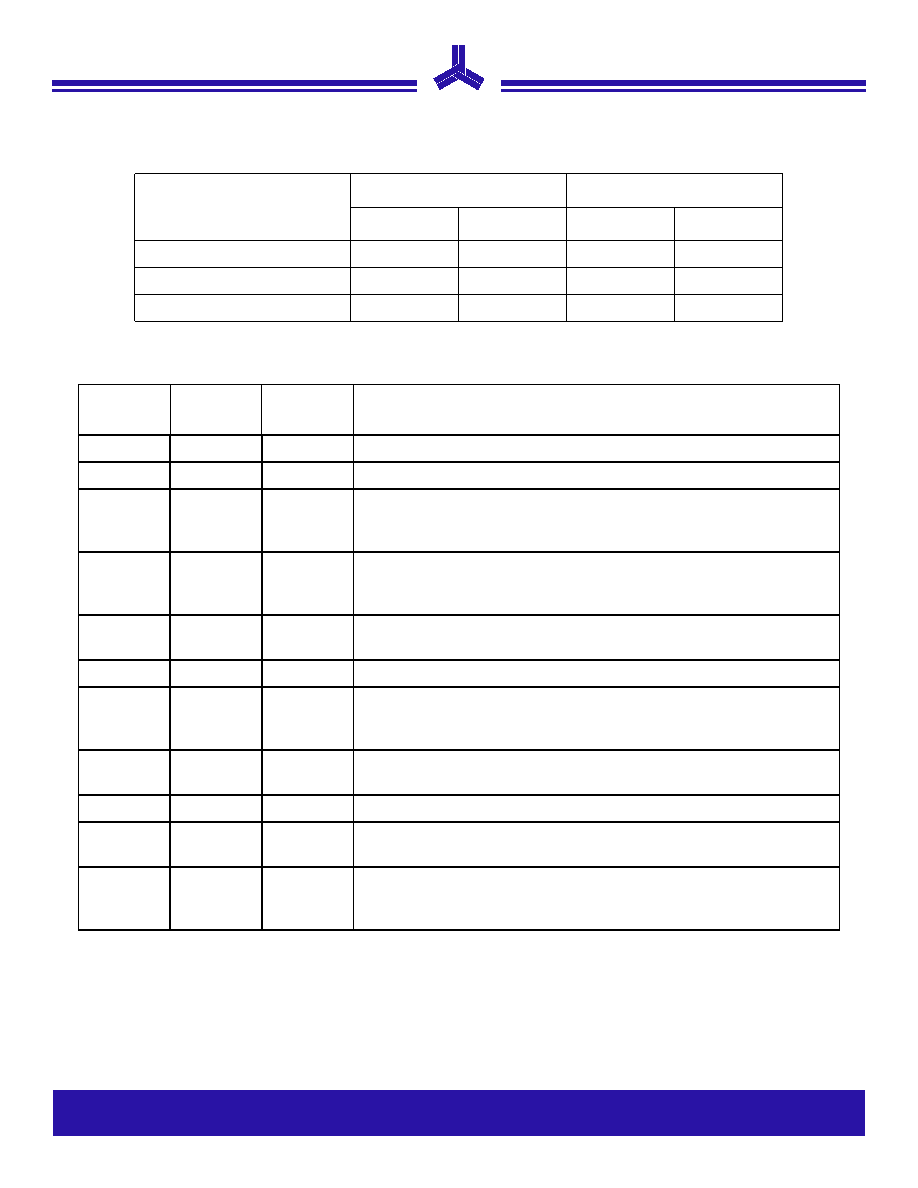
Frequency vs. Deviation (P1818A and P1818H)
Pin Description
Frequency
Deviation in P1818A
Deviation in P1818H
SRS = 1
SRS = 0
D_C = 1
D_C = 0
10 MHz
-4.4%
-3.3%
-4.4%
±2.2%
15 MHz
-1.8%
-1.26%
-1.8%
±0.9%
20 MHz
-0.8%
-0.6%
-0.8%
±0.4%
Pin
number
Name
Type
Description
1
XIN
I
Connect to externally generated clock signal or crystal.
2
VSS
P
Ground Connection. Connect to system ground.
3
SRS
I
Spread Range Select. Digital logic input used to select frequency devi-
ation (see Spread Deviation Selections). This pin has an internal pull-
up resistor.
3
1
1. Please refer to Figure 1 for pin assignment.
D_C
I
Digital logic input used to select Down (LOW) or Center (HIGH) Spread
Options (see Spread Deviation Selections). This pin has an internal
pull-up resistor.
4
ModOut
O
Spread Spectrum clock output (see Input Frequency and Modulation
Rate Selections and Spread Deviation Selections).
5
REF
O
Non-modulated reference output clock of the input frequency.
5/6
1
FRS
I
Frequency Range Select. Digital logic input used to select input fre-
quency range (see Input Frequency and Modulation Rate Selections).
This pin has an internal pull-up resistor.
6
1
PD#
I
Power-Down control pin. Pull LOW to enable Power-Down mode. This
pin has an internal pull-up resistor.
7
VDD
P
Connect to +3.3V
8
XOUT
I
Connect to crystal. No connect if externally generated clock signal is
used.
8
1
MRS
I
Modulation Rate Select. Digital logic input used to select Modulation
Rate (see Spread Deviation Selections). This pin has an internal pull-
up resistor.
Æ
Low Power Mobile VGA EMI Reduction IC
5 of 8
March 2003
P1818/19/20/21/22
Notice: The information in this document is subject to change without notice.
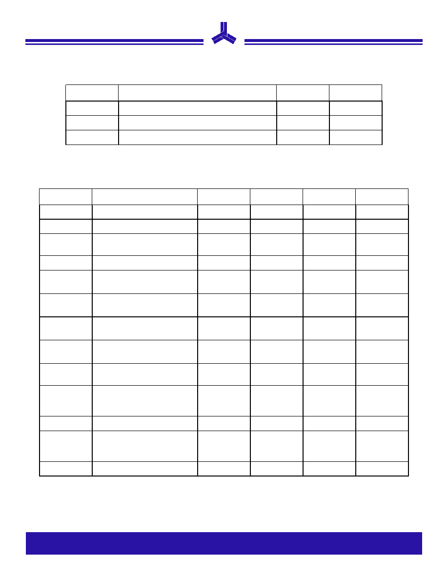
Absolute Maximum Ratings
DC Electrical Characteristics
3.3 V, 25
∞
C
Symbol
Parameter
Rating
Unit
V
DD
, V
IN
Voltage on any pin with respect to GND
-0.5 to +7.0
V
T
STG
Storage temperature
-65 to +125
∫ C
T
A
Operating temperature
0 to +70
∫ C
Symbol
Parameter
Min
Typ
Max
Unit
V
IL
Input low voltage
GND ≠ 0.3
≠
0.8
V
V
IH
Input high voltage
2.00
≠
V
DD
+ 0.3
V
I
IL
Input low current (inputs D_C,
PD#, MRS, FRS, SRS)
-60.0
≠
-20.00
µ
A
I
IH
Input high current
≠
≠
1.00
µ
A
I
XOL
XOUT output low current
(@ 0.4 V, V
DD
= 3.3 V)
2.00
≠
12.00
mA
I
XOH
XOUT output high current
(@ 2.5 V, V
DD
= 3.3 V)
≠
≠
12.00
mA
V
OL
Output low voltage
(V
DD
=3.3 V, I
OL
= 20 mA)
≠
≠
0.4
V
V
OH
Output high voltage
(V
DD
=3.3 V, I
OH
= 20 mA)
≠
≠
2.8
V
I
DD
Static supply current
Standby mode
≠
4.5
≠
mA
I
CC
Dynamic supply current
Normal mode (3.3 V and 25 pF
probe loading)
7.1
f
IN-min
≠
26.9
f
IN-max
mA
V
DD
Operating voltage
≠
3.3
≠
V
t
ON
Power up time
(first locked clock cycle after
power up)
≠
0.18
≠
mS
Z
OUT
Clock output impedance
≠
50
≠