November 2003
P2010A
rev F
Alliance Semiconductor
2575, Augustine Drive
∑ Santa Clara, CA ∑ Tel: 408.855.4900 ∑ Fax: 408.855.4999 ∑ www.alsc.com
Notice: The information in this document is subject to change without notice.
Low Frequency EMI Reduction IC
Features
FCC approved method of EMI attenuation
Provides up to 20 dB of EMI suppression
Generates a low EMI spread spectrum clock
of the input frequency
Optimized for 10 MHz to 35MHz input
frequency range
Internal loop filter minimizes external
components and board space
4 selectable spread ranges
SSON control pin for spread spectrum
enable and disable options
Characterizes to work with EMI-Lator
Æ
, EMC
simulation program.
Low cycle-to-cycle jitter
Wide operating range (3V to 5V)
16 mA output drives
TTL or CMOS compatible outputs
Low power CMOS design
Available in 8 pin SOIC and TSSOP
Product Description
The P2010 is a selectable spread spectrum
frequency modulator designed specifically for PC
peripheral and embedded controller markets. The
P2010 reduces electromagnetic interference (EMI) at
the clock source which provides system wide
reduction of EMI of all clock dependent signals. The
P2010 allows significant system cost savings by
reducing the number of circuit board layers and
shielding that are traditionally required to pass EMI
regulations.
The P2010 uses the most efficient and optimized
modulation profile approved by the FCC and is
implemented in a proprietary all-digital method.
The P2010 modulates the output of a single PLL in
order to "spread" the bandwidth of a synthesized
clock and, more importantly, decreases the peak
amplitudes of its harmonics. This results in
significantly lower system EMI compared to the
typical narrow band signal produced by oscillators
and most frequency generators. Lowering EMI by
increasing a signal's bandwidth is called "spread
spectrum clock generation".
Applications
The P2010 is targeted towards the embedded
controller market and PC peripheral markets
including scanners, facsimile, MFP's, printers, PDA,
IA, and GPS devices.
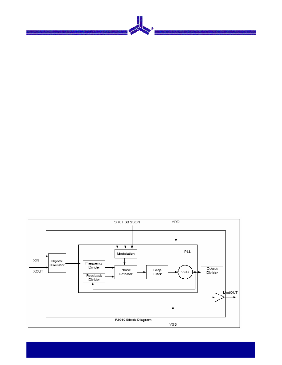
Block Diagram

November 2003
P2010A
rev F
Low Frequency EMI Reduction IC
2 of 9
Notice: The information in this document is subject to change without notice.
Pin Configuration
Pin Description
Pin#
Pin Name
Type
Description
1
XIN/CLK
I
Connect to crystal or externally generated clock signal.
2
XOUT
I
Connect to crystal. No connect if externally generated clock signal is used.
3 FS0 I
Digital logic input used to select Input Frequency Range (see Table 1). This
pin has an internal pull-up resistor.
4
VSS
P
Ground Connection. Connect to system ground.
5 SSON I
Digital logic input used to enable Spread Spectrum function (Active Low).
Spread Spectrum function enable when low. This pin has an internal pull-
low resistor.
6
ModOUT
O
Spread Spectrum Clock Output.
7 SR0 I
Digital logic input used to select Spreading Range (see Table 1). This pin
has an internal pull-up resistor.
8
VDD
P
Connect to +3.3V or +5.0V
Table 1 - Spread Range Selection
FS0
SR0
Spreading Range
Input Frequency
Modulation rate
1
0
+/- 1.50%
10 MHz to 20 MHz
(Fin/10)*20.83 KHz
1
1
+/- 2.50%
10 MHz to 20 MHz
(Fin/10)*20.83 KHz
0
0
+/- 1.25%
20 MHz to 35 MHz
(Fin/10)*20.83 KHz
0
1
+/- 2.00%
20 MHz to 35 MHz
(Fin/10)*20.83 KHz

November 2003
P2010A
rev F
Low Frequency EMI Reduction IC
3 of 9
Notice: The information in this document is subject to change without notice.
Spread Spectrum Selection
Table 1 illustrates the possible spread spectrum options. The optimal setting should minimize system EMI to the
fullest without affecting system performance. The spreading is described as a percentage deviation of the
center frequency (Note: the center frequency is the frequency of the external reference input on CLKIN, Pin 1).
Example of a typical printer or scanner application that operates on a clock frequency of 16 MHz:
A spreading selection of FS0=1 and SR0=1 provides a percentage deviation of +/-2.50%* (see Table 1) of F
cen
.
This results in the frequency on ModOUT being swept from 16.40 MHz to 15.60 MHz at a modulation rate of
33.33 KHz (see Table 1). This particular example (see Figure below) given here is a common EMI reduction
method for scanner, printer, or embedded applications and has already been adopted by most of the leading
manufacturers.
NOTE: Spreading range selection varies from different system manufacturers and their designs.
P2010 Application Schematic for Flat-Bed Scanner

November 2003
P2010A
rev F
Low Frequency EMI Reduction IC
4 of 9
Notice: The information in this document is subject to change without notice.
EMC Software Simulation
By using Alliance Semiconductor's proprietary EMC simulation software ≠ EMI-latorÆ, radiated system level EMI
analysis can be made easier to allow a quantitative assessment on Alliance's EMI reduction products. The
simulation engine of this EMC software has already been characterized to correlate with the electrical
characteristics of Alliance EMI reduction IC's. The figure below is an example of the simulation result. Please
visit our web site at
www.alsc.com
for information on how to obtain a free copy and demonstration of EMI-latorÆ.
Simulation Result from EMI-latorÆ

November 2003
P2010A
rev F
Low Frequency EMI Reduction IC
5 of 9
Notice: The information in this document is subject to change without notice.
Absolute Maximum Ratings
Symbol
Parameter
Rating
Unit
V
DD
, V
IN
Voltage on any pin with respect to GND
-0.5 to + 7.0
V
T
STG
Storage
temperature
-65 to +125
∞C
T
A
Operating
temperature
0 to +70
∞C
DC Electrical Characteristics
Symbol
Parameter
Min
Typ
Max
Unit
V
IL
Input Low Voltage
GND ≠
-
0.8
V
V
IH
Input High Voltage
2.0
-
V
DD
+ 0.3
V
I
IL
Input Low Current (pull-up resistor on inputs SR0, 1)
-
-
-35
µA
I
IH
Input High Current (pull-down resistor on input SSON)
-
-
35
µA
V
OL
Output Low Voltage (V
DD
=3.3V, I
OL
= 20 mA)
-
-
0.4
V
V
OH
Output High Voltage (V
DD
=3.3V, I
OH
= 20 mA)
2.5
-
-
V
I
DD
Static Supply Current
-
0.6
-
mA
I
CC
Dynamic Supply Current (3.3V and 15pF loading)
4
6
8
mA
V
DD
Operating
Voltage
2.7 3.3 5.5 V
t
ON
Power Up Time (First locked clock cycle after power
up)
0.18
ms
Z
OUT
Clock Output Impedance
50
AC Electrical Characteristics
Symbol
Parameter
Min
Typ
Max
Unit
f
IN
Input Frequency when
10
20
30
MHz
t
LH
*
Output rise time
(Measured at 0.8V to 2.0V)
0.7
0.9
1.1
ns
t
HL
*
Output fall time
(Measured at 0.8V to 2.0V)
0.6
0.8
1.0
ns
t
JC
Jitter (cycle to cycle)
-
-
360
ps
t
D
Output duty cycle
45
50
55
%
*t
LH
and t
HL
are measured into a capacitive load of 15pF