�
Altera Corporation
1
Cyclone
FPGA Family
March 2003, ver. 1.1
Data Sheet
DS-CYCLONE-1.1
Introduction
Preliminary
Information
The Cyclone
TM
field programmable gate array family is based on a 1.5-V,
0.13-
�
m, all-layer copper SRAM process, with densities up to 20,060 logic
elements (LEs) and up to 288 Kbits of RAM. With features like phase-
locked loops (PLLs) for clocking and a dedicated double data rate (DDR)
interface to meet DDR SDRAM and fast cycle RAM (FCRAM) memory
requirements, Cyclone devices are a cost-effective solution for data-path
applications. Cyclone devices support various I/O standards, including
LVDS at data rates up to 311 megabits per second (Mbps) and 66-MHz,
32-bit peripheral component interconnect (PCI), for interfacing with and
supporting ASSP and ASIC devices. Altera also offers new low-cost serial
configuration devices to configure Cyclone devices.
Features...
2,910 to 20,060 LEs, see
Table 1
Up to 294,912 RAM bits (36,864 bytes)
Supports configuration through low-cost serial configuration device
Support for LVTTL, LVCMOS, SSTL-2, and SSTL-3 I/O standards
Support for 66-MHz, 32-bit PCI standard
Low speed (311 Mbps) LVDS I/O support
Up to two PLLs per device provide clock multiplication and phase
shifting
Up to eight global clock lines with six clock resources available per
logic array block (LAB) row
Support for external memory, including DDR SDRAM (133 MHz),
FCRAM, and single data rate (SDR) SDRAM
Support for multiple intellectual property (IP) cores, including
Altera
MegaCore
functions and Altera Megafunctions Partners
Program (AMPP
SM
) megafunctions
Note to
Table 1
:
(1)
This parameter includes global clock pins.
Table 1. Cyclone Device Features
Feature
EP1C3
EP1C4
EP1C6
EP1C12
EP1C20
LEs
2,910
4,000
5,980
12,060
20,060
M4K RAM blocks (128
�
36 bits)
13
17
20
52
64
Total RAM bits
59,904
78,336
92,160
239,616
294,912
PLLs
1
2
2
2
2
Maximum user I/O pins
(1)
104
301
185
249
301
2
Altera Corporation
Cyclone FPGA Family Data Sheet
Preliminary Information
Cyclone devices are available in quad flat pack (QFP) and space-saving
FineLine BGA
packages (see
Tables 2
through
3
).
Notes to
Table 2
:
(1)
TQFP: thin quad flat pack.
PQFP: plastic quad flat pack.
(2)
Cyclone devices support vertical migration within the same package (i.e., designers can migrate between the EP1C3
device in the 144-pin TQFP package and the EP1C6 device in the same package).
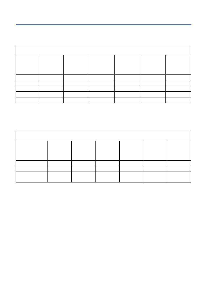
Table 2. Cyclone Package Options & I/O Pin Counts
Device
100-Pin
TQFP
(1)
144-Pin
TQFP
(1)
,
(2)
240-Pin
PQFP
(1)
256-Pin
FineLine
BGA
324-Pin
FineLine
BGA
400-Pin
FineLine
BGA
EP1C3
65
104
EP1C4
249
301
EP1C6
98
185
185
EP1C12
173
185
249
EP1C20
233
301
Table 3. Cyclone QFP & FineLine BGA Package Sizes
Dimension
100-Pin
TQFP
144-Pin
TQFP
240-Pin
PQFP
256-Pin
FineLine
BGA
324-Pin
FineLine
BGA
400-Pin
FineLine
BGA
Pitch (mm)
0.5
0.5
0.5
1.0
1.0
1.0
Area (mm
2
)
256
484
1,024
289
361
441
Length
�
width
(mm
�
mm)
16
�
16
22
�
22
34.6
�
34.6
17
�
17
19
�
19
21
�
21

4
Altera Corporation
Cyclone FPGA Family Data Sheet
Preliminary Information
Functional
Description
Cyclone devices contain a two-dimensional row- and column-based
architecture to implement custom logic. Column and row interconnects of
varying speeds provide signal interconnects between LABs and
embedded memory blocks.
The logic array consists of LABs, with 10 LEs in each LAB. An LE is a small
unit of logic providing efficient implementation of user logic functions.
LABs are grouped into rows and columns across the device. Cyclone
devices range between 2,910 to 20,060 LEs.
M4K RAM blocks are true dual-port memory blocks with 4K bits of
memory plus parity (4,608 bits). These blocks provide dedicated true
dual-port, simple dual-port, or single-port memory up to 36-bits wide at
up to 200 MHz. These blocks are grouped into columns across the device
in between certain LABs. Cyclone devices offer between 60 to 288 Kbits of
embedded RAM.
Each Cyclone device I/O pin is fed by an I/O element (IOE) located at the
ends of LAB rows and columns around the periphery of the device. I/O
pins support various single-ended and differential I/O standards, such as
the 66-MHz, 32-bit PCI standard and the LVDS I/O standard at up to
311 Mbps. Each IOE contains a bidirectional I/O buffer and three registers
for registering input, output, and output-enable signals. Dual-purpose
DQS, DQ, and DM pins along with delay chains (used to phase-align DDR
signals) provide interface support with external memory devices such as
DDR SDRAM, and FCRAM devices at up to 133 MHz (266 Mbps).
Cyclone devices provide a global clock network and up to two PLLs. The
global clock network consists of eight global clock lines that drive
throughout the entire device. The global clock network can provide clocks
for all resources within the device, such as IOEs, LEs, and memory blocks.
The global clock lines can also be used for control signals. Cyclone PLLs
provide general-purpose clocking with clock multiplication and phase
shifting as well as external outputs for high-speed differential I/O
support.
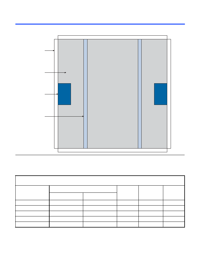
Figure 1
shows a diagram of the Cyclone EP1C12 device.
Altera Corporation
5
Preliminary Information
Cyclone FPGA Family Data Sheet
Figure 1. Cyclone EP1C12 Device Block Diagram
The number of M4K RAM blocks, PLLs, rows, and columns vary per
device.
Table 4
lists the resources available in each Cyclone device.
Logic Array
PLL
IOEs
M4K Blocks
EP1C12 Device
Table 4. Cyclone Device Resources
Device
M4K RAM
PLLs
LAB Columns
LAB Rows
Columns
Blocks
EP1C3
1
13
1
24
13
EP1C4
1
17
2
26
17
EP1C6
1
20
2
32
20
EP1C12
2
52
2
48
26
EP1C20
2
64
2
64
32