Document Outline
- ACEX 1K Programmable Logic Family Data Sheet

Æ
Altera Corporation
1
ACEX 1K
Programmable Logic Device Family
May 2003, ver. 3.4
Data Sheet
DS-ACEX-3.4
D
e
ve
l
o
pm
e
n
t
13
To
o
l
s
Features...
Programmable logic devices (PLDs), providing low cost
system-on-a-programmable-chip (SOPC) integration in a single
device
≠
Enhanced embedded array for implementing megafunctions
such as efficient memory and specialized logic functions
≠
Dual-port capability with up to 16-bit width per embedded array
block (EAB)
≠
Logic array for general logic functions
High density
≠
10,000 to 100,000 typical gates (see
Table 1
)
≠
Up to 49,152 RAM bits (4,096 bits per EAB, all of which can be
used without reducing logic capacity)
Cost-efficient programmable architecture for high-volume
applications
≠
Cost-optimized process
≠
Low cost solution for high-performance communications
applications
System-level features
≠
MultiVolt
TM
I/O pins can drive or be driven by 2.5-V, 3.3-V, or
5.0-V devices
≠
Low power consumption
≠
Bidirectional I/O performance (setup time [t
SU
] and clock-to-
output delay [t
CO
]) up to 250 MHz
≠
Fully compliant with the peripheral component interconnect
Special Interest Group (PCI SIG) PCI Local Bus Specification,
Revision 2.2
for 3.3-V operation at 33 MHz or 66 MHz
Extended temperature range
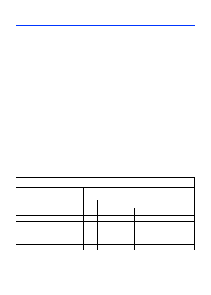
Table 1. ACEX
TM
1K Device Features
Feature
EP1K10
EP1K30
EP1K50
EP1K100
Typical gates
10,000
30,000
50,000
100,000
Maximum system gates
56,000
119,000
199,000
257,000
Logic elements (LEs)
576
1,728
2,880
4,992
EABs
3
6
10
12
Total RAM bits
12,288
24,576
40,960
49,152
Maximum user I/O pins
136
171
249
333

2
Altera Corporation
ACEX 1K Programmable Logic Device Family Data Sheet
...and More
Features
≠
-1 speed grade devices are compliant with PCI Local Bus
Specification, Revision 2.2
for 5.0-V operation
≠
Built-in Joint Test Action Group (JTAG) boundary-scan test
(BST) circuitry compliant with IEEE Std. 1149.1-1990, available
without consuming additional device logic.
≠
Operate with a 2.5-V internal supply voltage
≠
In-circuit reconfigurability (ICR) via external configuration
devices, intelligent controller, or JTAG port
≠
ClockLock
TM
and ClockBoost
TM
options for reduced clock delay,
clock skew, and clock multiplication
≠
Built-in, low-skew clock distribution trees
≠
100% functional testing of all devices; test vectors or scan chains
are not required
≠
Pull-up on I/O pins before and during configuration
Flexible interconnect
≠
FastTrack
Æ
Interconnect continuous routing structure for fast,
predictable interconnect delays
≠
Dedicated carry chain that implements arithmetic functions such
as fast adders, counters, and comparators (automatically used by
software tools and megafunctions)
≠
Dedicated cascade chain that implements high-speed,
high-fan-in logic functions (automatically used by software tools
and megafunctions)
≠
Tri-state emulation that implements internal tri-state buses
≠
Up to six global clock signals and four global clear signals
Powerful I/O pins
≠
Individual tri-state output enable control for each pin
≠
Open-drain option on each I/O pin
≠
Programmable output slew-rate control to reduce switching
noise
≠
Clamp to V
CCIO
user-selectable on a pin-by-pin basis
≠
Supports hot-socketing

Altera Corporation
3
ACEX 1K Programmable Logic Device Family Data Sheet
D
e
ve
l
o
pm
e
n
t
13
To
o
l
s
Software design support and automatic place-and-route provided by
Altera development systems for Windows-based PCs and Sun
SPARCstation, and HP 9000 Series 700/800 workstations
Flexible package options are available in 100 to 484 pins, including
the innovative FineLine BGA
TM
packages (see
Tables 2
and
3
)
Additional design entry and simulation support provided by EDIF
2 0 0 and 3 0 0 netlist files, library of parameterized modules (LPM),
DesignWare components, Verilog HDL, VHDL, and other interfaces
to popular EDA tools from manufacturers such as Cadence,
Exemplar Logic, Mentor Graphics, OrCAD, Synopsys, Synplicity,
VeriBest, and Viewlogic
Notes:
(1)
ACEX 1K device package types include thin quad flat pack (TQFP), plastic quad flat pack (PQFP), and FineLine
BGA packages.
(2)
Devices in the same package are pin-compatible, although some devices have more I/O pins than others. When
planning device migration, use the I/O pins that are common to all devices.
(3)
This option is supported with a 256-pin FineLine BGA package. By using SameFrame
TM
pin migration, all FineLine
BGA packages are pin-compatible. For example, a board can be designed to support 256-pin and 484-pin FineLine
BGA packages.
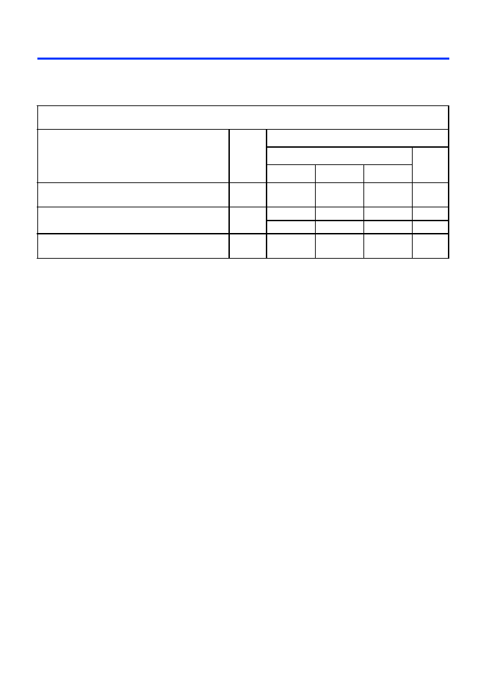
Table 2. ACEX 1K Package Options & I/O Pin Count
Notes (1)
,
(2)
Device
100-Pin TQFP
144-Pin TQFP
208-Pin PQFP
256-Pin
FineLine BGA
484-Pin
FineLine BGA
EP1K10
66
92
120
136
136
(3)
EP1K30
102
147
171
171
(3)
EP1K50
102
147
186
249
EP1K100
147
186
333
Table 3. ACEX 1K Package Sizes
Device
100-Pin TQFP
144-Pin TQFP
208-Pin PQFP
256-Pin
FineLine BGA
484-Pin
FineLine BGA
Pitch (mm)
0.50
0.50
0.50
1.0
1.0
Area (mm
2
)
256
484
936
289
529
Length
◊
width
(mm
◊
mm)
16
◊
16
22
◊
22
30.6
◊
30.6
17
◊
17
23
◊
23
4
Altera Corporation
ACEX 1K Programmable Logic Device Family Data Sheet
General
Description
Altera
Æ
ACEX 1K devices provide a die-efficient, low-cost architecture by
combining look-up table (LUT) architecture with EABs. LUT-based logic
provides optimized performance and efficiency for data-path, register
intensive, mathematical, or digital signal processing (DSP) designs, while
EABs implement RAM, ROM, dual-port RAM, or first-in first-out (FIFO)
functions. These elements make ACEX 1K suitable for complex logic
functions and memory functions such as digital signal processing, wide
data-path manipulation, data transformation and microcontrollers, as
required in high-performance communications applications. Based on
reconfigurable CMOS SRAM elements, the ACEX 1K architecture
incorporates all features necessary to implement common gate array
megafunctions, along with a high pin count to enable an effective interface
with system components. The advanced process and the low voltage
requirement of the 2.5-V core allow ACEX 1K devices to meet the
requirements of low-cost, high-volume applications ranging from DSL
modems to low-cost switches.
The ability to reconfigure ACEX 1K devices enables complete testing prior
to shipment and allows the designer to focus on simulation and design
verification. ACEX 1K device reconfigurability eliminates inventory
management for gate array designs and test vector generation for fault
coverage.
Table 4
shows ACEX 1K device performance for some common designs.
All performance results were obtained with Synopsys DesignWare or
LPM functions. Special design techniques are not required to implement
the applications; the designer simply infers or instantiates a function in a
Verilog HDL, VHDL, Altera Hardware Description Language (AHDL), or
schematic design file.
Notes:
(1)
This application uses combinatorial inputs and outputs.
(2)
This application uses registered inputs and outputs.
Table 4. ACEX 1K Device Performance
Application
Resources
Used
Performance
LEs
EABs
Speed Grade
Units
-1
-2
-3
16-bit loadable counter
16
0
285
232
185
MHz
16-bit accumulator
16
0
285
232
185
MHz
16-to-1 multiplexer
(1)
10
0
3.5
4.5
6.6
ns
16-bit multiplier with 3-stage pipeline
(2)
592
0
156
131
93
MHz
256
◊
16 RAM read cycle speed
(2)
0
1
278
196
143
MHz
256
◊
16 RAM write cycle speed
(2)
0
1
185
143
111
MHz
Altera Corporation
5
ACEX 1K Programmable Logic Device Family Data Sheet
D
e
ve
l
o
pm
e
n
t
13
To
o
l
s
Table 5
shows ACEX 1K device performance for more complex designs.
These designs are available as Altera MegaCore
TM
functions.
Each ACEX 1K device contains an embedded array and a logic array. The
embedded array is used to implement a variety of memory functions or
complex logic functions, such as digital signal processing (DSP), wide
data-path manipulation, microcontroller applications, and data-
transformation functions. The logic array performs the same function as
the sea-of-gates in the gate array and is used to implement general logic
such as counters, adders, state machines, and multiplexers. The
combination of embedded and logic arrays provides the high
performance and high density of embedded gate arrays, enabling
designers to implement an entire system on a single device.
ACEX 1K devices are configured at system power-up with data stored in
an Altera serial configuration device or provided by a system controller.
Altera offers EPC16, EPC2, EPC1, and EPC1441 configuration devices,
which configure ACEX 1K devices via a serial data stream. Configuration
data can also be downloaded from system RAM or via the Altera
MasterBlaster
TM
, ByteBlasterMV
TM
, or BitBlaster
TM
download cables. After
an ACEX 1K device has been configured, it can be reconfigured in-circuit
by resetting the device and loading new data. Because reconfiguration
requires less than 40 ms, real-time changes can be made during system
operation.
ACEX 1K devices contain an interface that permits microprocessors to
configure ACEX 1K devices serially or in parallel, and synchronously or
asynchronously. The interface also enables microprocessors to treat an
ACEX 1K device as memory and configure it
by writing to a virtual
memory location, simplifying device reconfiguration.
Table 5. ACEX 1K Device Performance for Complex Designs
Application
LEs
Used
Performance
Speed Grade
Units
-1
-2
-3
16-bit, 8-tap parallel finite impulse response (FIR)
filter
597
192
156
116
MSPS
8-bit, 512-point Fast Fourier transform (FFT)
function
1,854
23.4
28.7
38.9
µ
s
113
92
68
MHz
a16450
universal asynchronous
receiver/transmitter (UART)
342
36
28
20.5
MHz