APEX II Programmable Logic Device Family Data Sheet

®
Altera Corporation
1
APEX II
Programmable Logic
Device Family
August 2002, ver. 3.0
Data Sheet
DS-APEXII-3.0
Features...
Programmable logic device (PLD) manufactured using a 0.15-
µ
m all-
layer copper-metal fabrication process (up to eight layers of metal)
1-gigabit per second (Gbps) True-LVDS
TM
, LVPECL, pseudo
current mode logic (PCML), and HyperTransport
TM
interface
Clock-data synchronization (CDS) in True-LVDS interface to
correct any fixed clock-to-data skew
Enables common networking and communications bus I/O
standards such as RapidIO
TM
, CSIX, Utopia IV, and POS-PHY
Level 4
Support for high-speed external memory interfaces, including
zero bus turnaround (ZBT), quad data rate (QDR), and double
data rate (DDR) static RAM (SRAM), and single data rate (SDR)
and DDR synchronous dynamic RAM (SDRAM)
30% to 40% faster design performance than APEX
TM
20KE
devices on average
Enhanced 4,096-bit embedded system blocks (ESBs)
implementing first-in first-out (FIFO) buffers, Dual-Port+ RAM
(bidirectional dual-port RAM), and content-addressable
memory (CAM)
High-performance, low-power copper interconnect
Fast parallel byte-wide synchronous device configuration
Look-up table (LUT) logic available for register-intensive
functions
High-density architecture
1,900,000 to 5,250,000 maximum system gates (see
Table 1
)
Up to 67,200 logic elements (LEs)
Up to 1,146,880 RAM bits that can be used without reducing
available logic
Low-power operation design
1.5-V supply voltage
Copper interconnect reduces power consumption
MultiVolt
TM
I/O support for 1.5-V, 1.8-V, 2.5-V, and 3.3-V
interfaces
ESBs offer programmable power-saving mode
2
Altera Corporation
APEX II Programmable Logic Device Family Data Sheet
Notes to
Table 1
:
(1)
Each device has 36 input channels and 36 output channels.
(2)
EP2A15 and EP2A25 devices have 56 input and 56 output channels; EP2A40 and EP2A70 devices have 88 input and
88 output channels.
(3)
PLL: phase-locked loop. True-LVDS PLLs are dedicated to implement True-LVDS functionality.
(4)
Two internal outputs per PLL are available. Additionally, the device has one external output per PLL pair (two
external outputs per device).
...and More
Features
I/O features
Up to 380 Gbps of I/O capability
1-Gbps True-LVDS, LVPECL, PCML, and HyperTransport
support on 36 input and 36 output channels that feature clock
synchronization circuitry and independent clock multiplication
and serialization/deserialization factors
Common networking and communications bus I/O standards
such as RapidIO, CSIX, Utopia IV, and POS-PHY Level 4 enabled
400-megabits per second (Mbps) Flexible-LVDS and
HyperTransport support on up to 88 input and 88 output
channels (input channels also support LVPECL)
Support for high-speed external memories, including ZBT, QDR,
and DDR SRAM, and SDR and DDR SDRAM
Compliant with peripheral component interconnect Special
Interest Group (PCI SIG) PCI Local Bus Specification,
Revision 2.2
for 3.3-V operation at 33 or 66 MHz and 32 or 64 bits
Compliant with 133-MHz PCI-X specifications
Support for other advanced I/O standards, including AGP, CTT,
SSTL-3 and SSTL-2 Class I and II, GTL+, and HSTL Class I and II
Six dedicated registers in each I/O element (IOE): two input
registers, two output registers, and two output-enable registers
Programmable bus hold feature
Programmable pull-up resistor on I/O pins available during
user mode
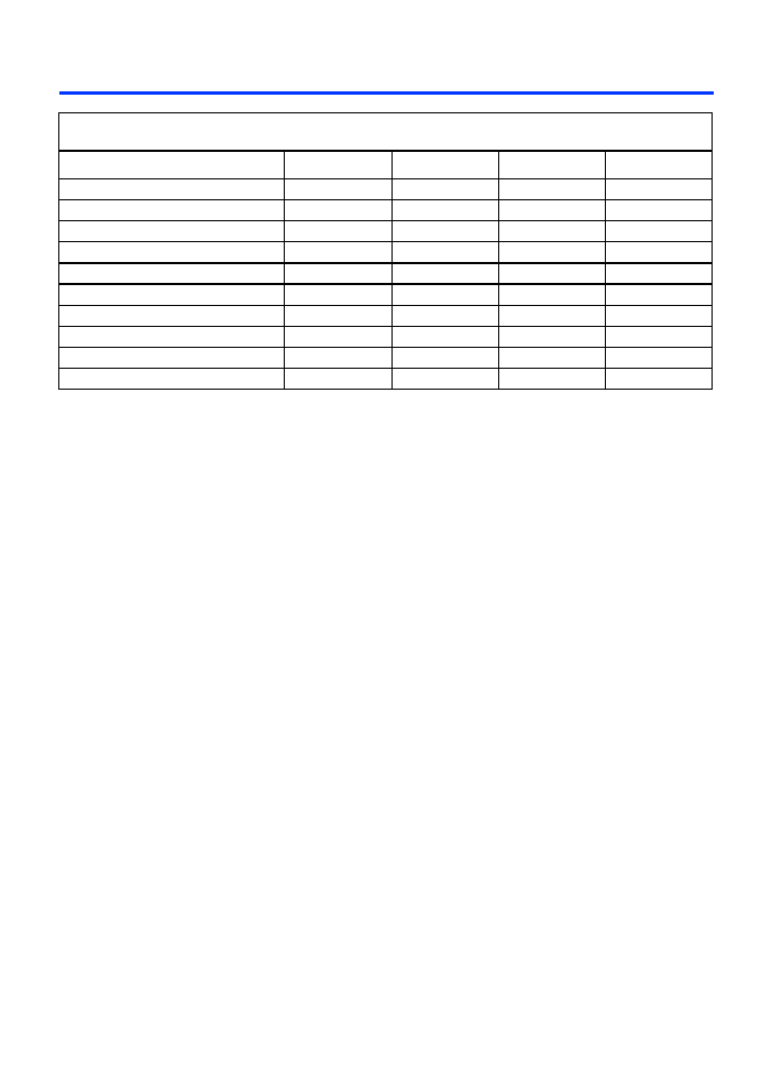
Table 1. APEX II Device Features
Feature
EP2A15
EP2A25
EP2A40
EP2A70
Maximum gates
1,900,000
2,750,000
3,000,000
5,250,000
Typical gates
600,000
900,000
1,500,000
3,000,000
LEs
16,640
24,320
38,400
67,200
RAM ESBs
104
152
160
280
Maximum RAM bits
425,984
622,592
655,360
1,146,880
True-LVDS channels
36
(1)
36
(1)
36
(1)
36
(1)
Flexible-LVDS
TM
channels
(2)
56
56
88
88
True-LVDS PLLs
(3)
4
4
4
4
General-purpose PLL outputs
(4)
8
8
8
8
Maximum user I/O pins
492
612
735
1,060

Altera Corporation
3
APEX II Programmable Logic Device Family Data Sheet
Programmable output drive for 3.3-V LVTTL at 4 mA, 12 mA,
24 mA, or I/O standard levels
Programmable output slew-rate control reduces switching noise
Hot-socketing operation supported
Pull-up resistor on I/O pins before and during configuration
Enhanced internal memory structure
High-density 4,096-bit ESBs
Dual-Port+ RAM with bidirectional read and write ports
Support for many other memory functions, including CAM,
FIFO, and ROM
ESB packing mode partitions one ESB into two 2,048-bit blocks
Device configuration
Fast byte-wide synchronous configuration minimizes in-circuit
reconfiguration time
Device configuration supports multiple voltages (either 3.3 V
and 2.5 V or 1.8 V)
Flexible clock management circuitry with eight general-purpose PLL
outputs
Four general-purpose PLLs with two outputs per PLL
Built-in low-skew clock tree
Eight global clock signals
ClockLock
TM
feature reducing clock delay and skew
ClockBoost
TM
feature providing clock multiplication (by 1 to 160)
and division (by 1 to 256)
ClockShift
TM
feature providing programmable clock phase and
delay shifting with coarse (90°, 180°, or 270°) and fine (0.5 to
1.0 ns) resolution
Advanced interconnect structure
All-layer copper interconnect for high performance
Four-level hierarchical FastTrack
®
interconnect structure for fast,
predictable interconnect delays
Dedicated carry chain that implements arithmetic functions such
as fast adders, counters, and comparators (automatically used by
software tools and megafunctions)
Dedicated cascade chain that implements high-speed,
high-fan-in logic functions (automatically used by software tools
and megafunctions)
Interleaved local interconnect allowing one LE to drive 29 other
LEs through the fast local interconnect
Advanced software support
Software design support and automatic place-and-route
provided by the Altera
®
Quartus
TM
II development system for
Windows-based PCs, Sun SPARCstations, and HP 9000
Series 700/800 workstations
Altera MegaCore
®
functions and Altera Megafunction Partners
Program (AMPP
SM
) megafunctions optimized for APEX II
architecture
4
Altera Corporation
APEX II Programmable Logic Device Family Data Sheet
LogicLock
TM
incremental design for intellectual property (IP)
integration and team-based design
NativeLink
TM
integration with popular synthesis, simulation,
and timing analysis tools
SignalTap
®
embedded logic analyzer simplifies in-system design
evaluation by giving access to internal nodes during device
operation
Support for popular revision-control software packages,
including PVCS, RCS, and SCCS
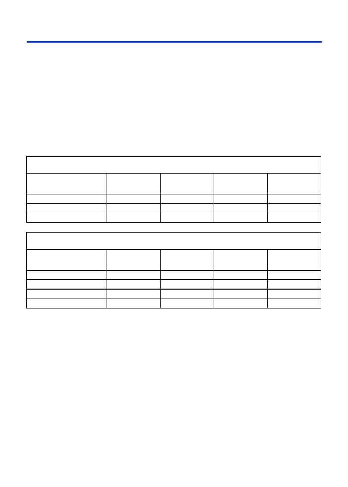
Tables 2
and
3
show the APEX II ball-grid array (BGA) and
FineLine BGA
TM
device package sizes, options, and I/O pin counts.
Notes to
Table 3
:
(1)
All APEX II devices support vertical migration within the same package (e.g., the designer can migrate between the
EP2A15, EP2A25, and EP2A40 devices in the 672-pin FineLine BGA package). Vertical migration means that
designers can migrate to devices whose dedicated pins, configuration pins, LVDS pins, and power pins are the same
for a given package across device densities. Migration of I/O pins across densities requires the designer to cross
reference the available I/O pins using the device pin-outs. This must be done for all planned densities for a given
package type to identify which I/O pins are migratable.
(2)
I/O pin counts include dedicated clock and fast I/O pins.
Table 2. APEX II Package Sizes
Feature
672-Pin
FineLine BGA
724-Pin BGA
1,020-Pin
FineLine BGA
1,508-Pin
FineLine BGA
Pitch (mm)
1.00
1.27
1.00
1.00
Area (mm
2
)
729
1,225
1,089
1,600
Length
×
Width (mm
×
mm)
27
×
27
35
×
35
33
×
33
40
×
40
Table 3. APEX II Package Options & I/O Pin Count
Notes (1)
,
(2)
Feature
672-Pin
FineLine BGA
724-Pin BGA
1,020-Pin
FineLine BGA
1,508-Pin
FineLine BGA
EP2A15
492
492
EP2A25
492
536
EP2A40
492
536
735
EP2A70
536
1,060

Altera Corporation
5
APEX II Programmable Logic Device Family Data Sheet
General
Description
APEX II devices integrate high-speed differential I/O support using the
True-LVDS interface. The dedicated serializer, deserializer, and CDS
circuitry in the True-LVDS interface support the LVDS, LVPECL,
HyperTransport, and PCML I/O standards. Flexible-LVDS pins located
in regular user I/O banks offer additional differential support, increasing
the total device bandwidth. This circuitry, together with enhanced IOEs
and support for numerous I/O standards, allows APEX II devices to meet
high-speed interface requirements.
APEX II devices also include other high-performance features such as
bidirectional dual-port RAM, CAM, general-purpose PLLs, and
numerous global clocks.
Configuration
The logic, circuitry, and interconnects in the APEX II architecture are
configured with CMOS SRAM elements. APEX II devices are
reconfigurable and are 100% tested prior to shipment. As a result, test
vectors do not have to be generated for fault coverage. Instead, the
designer can focus on simulation and design verification. In addition, the
designer does not need to manage inventories of different ASIC designs;
APEX II devices can be configured on the board for the specific
functionality required.
APEX II devices are configured at system power-up with data either
stored in an Altera configuration device or provided by a system
controller. Altera offers in-system programmability (ISP)-capable
configuration devices, which configure APEX II devices via a serial data
stream. The enhanced configuration devices can configure any APEX II
device in under 100 ms. Moreover, APEX II devices contain an optimized
interface that permits microprocessors to configure APEX II devices
serially or in parallel, synchronously or asynchronously. This interface
also enables microprocessors to treat APEX II devices as memory and to
configure the device by writing to a virtual memory location, simplifying
reconfiguration.
APEX II devices also support a new byte-wide, synchronous
configuration scheme at speeds of up to 66 MHz using EPC16
configuration devices or a microprocessor. This parallel configuration
reduces configuration time by using eight data lines to send configuration
data versus one data line in serial configuration.
APEX II devices support multi-voltage configuration; device
configuration can be performed at 3.3 V and 2.5 V or 1.8 V.
Document Outline
- APEX II Programmable Logic Device Family Data Sheet