Document Outline
- FLEX 8000 Programmable Logic Device Family Data Sheet
Æ
Altera Corporation
1
FLEX 8000
Programmable Logic
Device Family
January 2003, ver. 11.1
Data Sheet
DS-F8000-11.1
FL
EX 800
0
3
1
Features...
Low-cost, high-density, register-rich CMOS programmable logic
device (PLD) family (see
Table 1
)
≠
2,500 to 16,000 usable gates
≠
282 to 1,500 registers
System-level features
≠
In-circuit reconfigurability (ICR) via external configuration
devices or intelligent controller
≠
Fully compliant with the peripheral component interconnect
Special Interest Group (PCI SIG) PCI Local Bus Specification,
Revision 2.2
for 5.0-V operation
≠
Built-in Joint Test Action Group (JTAG) boundary-scan test (BST)
circuitry compliant with IEEE Std. 1149.1-1990 on selected devices
≠
MultiVolt
TM
I/O interface enabling device core to run at 5.0 V,
while I/O pins are compatible with 5.0-V and 3.3-V logic levels
≠
Low power consumption (typical specification is 0.5 mA or less in
standby mode)
Flexible interconnect
≠
FastTrack
Æ
Interconnect continuous routing structure for fast,
predictable interconnect delays
≠
Dedicated carry chain that implements arithmetic functions such
as fast adders, counters, and comparators (automatically used by
software tools and megafunctions)
≠
Dedicated cascade chain that implements high-speed, high-fan-in
logic functions (automatically used by software tools and
megafunctions)
≠
Tri-state emulation that implements internal tri-state nets
Powerful I/O pins
Programmable output slew-rate control reduces switching noise
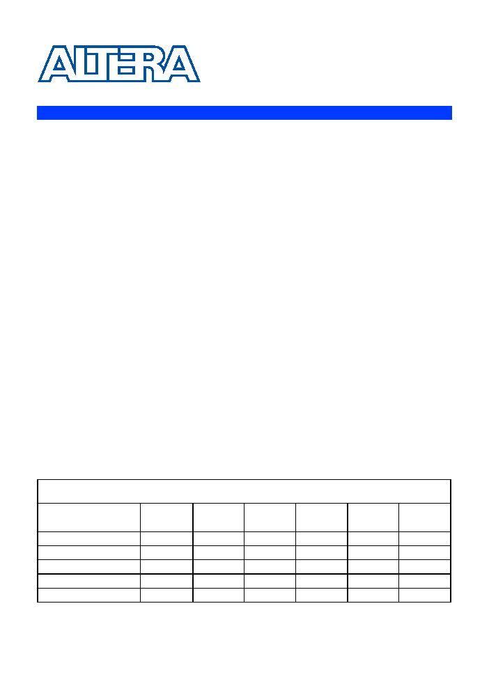
Table 1. FLEX 8000 Device Features
Feature
EPF8282A
EPF8282AV
EPF8452A
EPF8636A
EPF8820A
EPF81188A EPF81500A
Usable gates
2,500
4,000
6,000
8,000
12,000
16,000
Flipflops
282
452
636
820
1,188
1,500
Logic array blocks (LABs)
26
42
63
84
126
162
Logic elements (LEs)
208
336
504
672
1,008
1,296
Maximum user I/O pins
78
120
136
152
184
208

2
Altera Corporation
FLEX 8000 Programmable Logic Device Family Data Sheet
...and More
Features
Peripheral register for fast setup and clock-to-output delay
Fabricated on an advanced SRAM process
Available in a variety of packages with 84 to 304 pins (see
Table 2
)
Software design support and automatic place-and-route provided by
the Altera
Æ
MAX+PLUS
Æ
II development system for Windows-based
PCs, as well as Sun SPARCstation, HP 9000 Series 700/800, and IBM
RISC System/6000 workstations
Additional design entry and simulation support provided by EDIF
2 0 0 and 3 0 0 netlist files, library of parameterized modules (LPM),
Verilog HDL, VHDL, and other interfaces to popular EDA tools from
manufacturers such as Cadence, Exemplar Logic, Mentor Graphics,
OrCAD, Synopsys, Synplicity, and Veribest
Note:
(1)
FLEX 8000 device package types include plastic J-lead chip carrier (PLCC), thin quad flat pack (TQFP), plastic quad
flat pack (PQFP), power quad flat pack (RQFP), ball-grid array (BGA), and pin-grid array (PGA) packages.
General
Description
Altera's Flexible Logic Element MatriX (FLEX
Æ
) family combines the
benefits of both erasable programmable logic devices (EPLDs) and field-
programmable gate arrays (FPGAs). The FLEX 8000 device family is ideal
for a variety of applications because it combines the fine-grained
architecture and high register count characteristics of FPGAs with the
high speed and predictable interconnect delays of EPLDs. Logic is
implemented in LEs that include compact 4-input look-up tables (LUTs)
and programmable registers. High performance is provided by a fast,
continuous network of routing resources.
JTAG BST circuitry
Yes
No
Yes
Yes
No
Yes
Table 2. FLEX 8000 Package Options & I/O Pin Count
Note (1)
Device
84-
Pin
PLCC
100-
Pin
TQFP
144-
Pin
TQFP
160-
Pin
PQFP
160-
Pin
PGA
192-
Pin
PGA
208-
Pin
PQFP
225-
Pin
BGA
232-
Pin
PGA
240-
Pin
PQFP
280-
Pin
PGA
304-
Pin
RQFP
EPF8282A
68
78
EPF8282AV
78
EPF8452A
68
68
120
120
EPF8636A
68
118
136
136
EPF8820A
112
120
152
152
152
EPF81188A
148
184
184
EPF81500A
181
208
208

Altera Corporation
3
FLEX 8000 Programmable Logic Device Family Data Sheet
FL
EX 800
0
3
FLEX 8000 devices provide a large number of storage elements for
applications such as digital signal processing (DSP), wide-data-path
manipulation, and data transformation. These devices are an excellent
choice for bus interfaces, TTL integration, coprocessor functions, and
high-speed controllers. The high-pin-count packages can integrate
multiple 32-bit buses into a single device.
Table 3
shows FLEX 8000
performance and LE requirements for typical applications.
All FLEX 8000 device packages provide four dedicated inputs for
synchronous control signals with large fan-outs. Each I/O pin has an
associated register on the periphery of the device. As outputs, these
registers provide fast clock-to-output times; as inputs, they offer quick
setup times.
The logic and interconnections in the FLEX 8000 architecture are
configured with CMOS SRAM elements. FLEX 8000 devices are
configured at system power-up with data stored in an industry-standard
parallel EPROM or an Altera serial configuration devices, or with data
provided by a system controller. Altera offers the EPC1, EPC1213,
EPC1064, and EPC1441 configuration devices, which configure
FLEX 8000 devices via a serial data stream. Configuration data can also be
stored in an industry-standard 32 K
◊
8 bit or larger configuration device,
or downloaded from system RAM. After a FLEX 8000 device has been
configured, it can be reconfigured in-circuit by resetting the device and
loading new data. Because reconfiguration requires less than 100 ms, real-
time changes can be made during system operation. For information on
how to configure FLEX 8000 devices, go to the following documents:
Configuration Devices for APEX & FLEX Devices Data Sheet
BitBlaster Serial Download Cable Data Sheet
ByteBlasterMV Parallel Port Download Cable Data Sheet
Application Note 33 (Configuring FLEX 8000 Devices)
Application Note 38 (Configuring Multiple FLEX 8000 Devices)
Table 3. FLEX 8000 Performance
Application
LEs Used
Speed Grade
Units
A-2
A-3
A-4
16-bit loadable counter
16
125
95
83
MHz
16-bit up/down counter
16
125
95
83
MHz
24-bit accumulator
24
87
67
58
MHz
16-bit address decode
4
4.2
4.9
6.3
ns
16-to-1 multiplexer
10
6.6
7.9
9.5
ns

4
Altera Corporation
FLEX 8000 Programmable Logic Device Family Data Sheet
FLEX 8000 devices contain an optimized microprocessor interface that
permits the microprocessor to configure FLEX 8000 devices serially, in
parallel, synchronously, or asynchronously. The interface also enables the
microprocessor to treat a FLEX 8000 device as memory and configure the
device by writing to a virtual memory location, making it very easy for the
designer to create configuration software.
The FLEX 8000 family is supported by Altera's MAX+PLUS II
development system, a single, integrated package that offers schematic,
text--including the Altera Hardware Description Language (AHDL),
VHDL, and Verilog HDL--and waveform design entry, compilation and
logic synthesis, simulation and timing analysis, and device programming.
The MAX+PLUS II software provides EDIF 2 0 0 and 3 0 0, library of
parameterized modules (LPM), VHDL, Verilog HDL, and other interfaces
for additional design entry and simulation support from other industry-
standard PC- and UNIX workstation-based EDA tools. The
MAX+PLUS II software runs on Windows-based PCs and Sun
SPARCstation, HP 9000 Series 700/800, and IBM RISC System/6000
workstations.
The MAX+PLUS II software interfaces easily with common gate array
EDA tools for synthesis and simulation. For example, the MAX+PLUS II
software can generate Verilog HDL files for simulation with tools such as
Cadence Verilog-XL. Additionally, the MAX+PLUS II software contains
EDA libraries that use device-specific features such as carry chains, which
are used for fast counter and arithmetic functions. For instance, the
Synopsys Design Compiler library supplied with the MAX+PLUS II
development system includes DesignWare functions that are optimized
for the FLEX 8000 architecture.
f
For more information on the MAX+PLUS II software, go to the
MAX+PLUS II Programmable Logic Development System & Software Data
Sheet
.
Functional
Description
The FLEX 8000 architecture incorporates a large matrix of compact
building blocks called logic elements (LEs). Each LE contains a 4-input
LUT that provides combinatorial logic capability and a programmable
register that offers sequential logic capability. The fine-grained structure
of the LE provides highly efficient logic implementation.
Eight LEs are grouped together to form a logic array block (LAB). Each
FLEX 8000 LAB is an independent structure with common inputs,
interconnections, and control signals. The LAB architecture provides a
coarse-grained structure for high device performance and easy routing.

Altera Corporation
5
FLEX 8000 Programmable Logic Device Family Data Sheet
FL
EX 800
0
3
Figure 1
shows a block diagram of the FLEX 8000 architecture. Each group
of eight LEs is combined into an LAB; LABs are arranged into rows and
columns. The I/O pins are supported by I/O elements (IOEs) located at
the ends of rows and columns. Each IOE contains a bidirectional I/O
buffer and a flipflop that can be used as either an input or output register.
Figure 1. FLEX 8000 Device Block Diagram
Signal interconnections within FLEX 8000 devices and between device
pins are provided by the FastTrack Interconnect, a series of fast,
continuous channels that run the entire length and width of the device.
IOEs are located at the end of each row (horizontal) and column (vertical)
FastTrack Interconnect path.
IOE
IOE
IOE
IOE
IOE
IOE
IOE
IOE
IOE
IOE
IOE
IOE
IOE
IOE
IOE
IOE
I/O Element
(IOE)
Logic Array
Block (LAB)
Logic
Element (LE)
FastTrack
Interconnect