Document Outline
- MAX 7000B Programmable Logic Device Data Sheet

Æ
Altera Corporation
1
MAX 7000B
Programmable Logic
Device
November 2002, ver. 3.2
Data Sheet
DS-MAX7000B-3.2
Features...
High-performance 2.5-V CMOS EEPROM-based programmable logic
devices (PLDs) built on second-generation Multiple Array MatriX
(MAX
Æ
) architecture (see
Table 1
)
≠
Pin-compatible with the popular 5.0-V MAX 7000S and 3.3-V
MAX 7000A device families
≠
High-density PLDs ranging from 600 to 10,000 usable gates
≠
3.5-ns pin-to-pin logic delays with counter frequencies in excess
of 303.0 MHz
Advanced 2.5-V in-system programmability (ISP)
≠
Programs through the built-in IEEE Std. 1149.1 Joint Test Action
Group (JTAG) interface with advanced pin-locking capability
≠
Enhanced ISP algorithm for faster programming
≠
ISP_Done bit to ensure complete programming
≠
Pull-up resistor on I/O pins during in-system programming
≠
ISP circuitry compliant with IEEE Std. 1532
f
For information on in-system programmable 5.0-V MAX 7000S or 3.3-V
MAX 7000A devices, see the
MAX 7000 Programmable Logic Device Family
Data Sheet
or the
MAX 7000A Programmable Logic Device Family Data Sheet
.
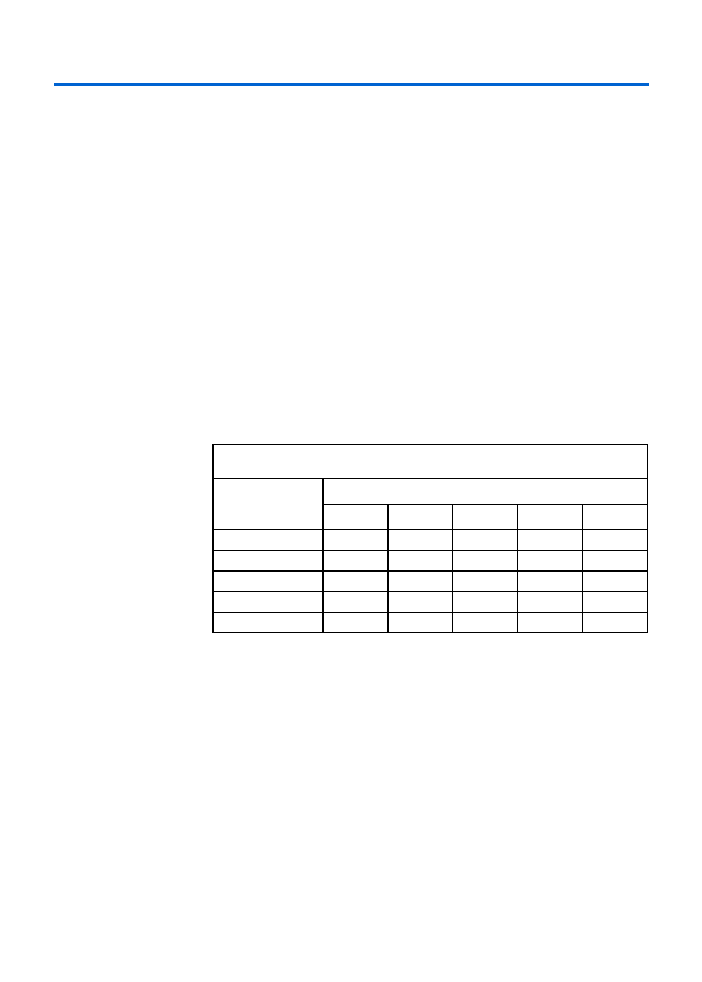
Table 1. MAX 7000B Device Features
Feature
EPM7032B
EPM7064B
EPM7128B
EPM7256B
EPM7512B
Usable gates
600
1,250
2,500
5,000
10,000
Macrocells
32
64
128
256
512
Logic array blocks
2
4
8
16
32
Maximum user I/O
pins
36
68
100
164
212
t
PD
(ns)
3.5
3.5
4.0
5.0
5.5
t
SU
(ns)
2.1
2.1
2.5
3.3
3.6
t
FSU
(ns)
1.0
1.0
1.0
1.0
1.0
t
CO1
(ns)
2.4
2.4
2.8
3.3
3.7
f
CNT
(MHz)
303.0
303.0
243.9
188.7
163.9

2
Altera Corporation
MAX 7000B Programmable Logic Device Data Sheet
...and More
Features
System-level features
≠
MultiVolt
TM
I/O interface enabling device core to run at 2.5 V,
while I/O pins are compatible with 3.3-V, 2.5-V, and 1.8-V logic
levels
≠
Programmable power-saving mode for 50% or greater power
reduction in each macrocell
≠
Fast input setup times provided by a dedicated path from I/O
pin to macrocell registers
≠
Support for advanced I/O standards, including SSTL-2 and
SSTL-3, and GTL+
≠
Bus-hold option on I/O pins
≠
PCI compatible
≠
Bus-friendly architecture including programmable slew-rate
control
≠
Open-drain output option
≠
Programmable security bit for protection of proprietary designs
≠
Built-in boundary-scan test circuitry compliant with
IEEE Std. 1149.1
≠
Supports hot-socketing operation
≠
Programmable ground pins
Advanced architecture features
≠
Programmable interconnect array (PIA) continuous routing
structure for fast, predictable performance
≠
Configurable expander product-term distribution, allowing up
to 32 product terms per macrocell
≠
Programmable macrocell registers with individual clear, preset,
clock, and clock enable controls
≠
Two global clock signals with optional inversion
≠
Programmable power-up states for macrocell registers
≠
6 to 10 pin- or logic-driven output enable signals
Advanced package options
≠
Pin counts ranging from 44 to 256 in a variety of thin quad flat
pack (TQFP), plastic quad flat pack (PQFP), ball-grid array
(BGA), space-saving FineLine BGA
TM
, 0.8-mm Ultra
FineLine BGA, and plastic J-lead chip carrier (PLCC) packages
≠
Pin-compatibility with other MAX 7000B devices in the same
package
Advanced software support
≠
Software design support and automatic place-and-route
provided by Altera's MAX+PLUS
Æ
II development system for
Windows-based PCs and Sun SPARCstation, and HP 9000
Series 700/800 workstations
Altera Corporation
3
MAX 7000B Programmable Logic Device Data Sheet
≠
Additional design entry and simulation support provided by
EDIF 2 0 0 and 3 0 0 netlist files, library of parameterized
modules (LPMs), Verilog HDL, VHDL, and other interfaces to
popular EDA tools from manufacturers such as Cadence,
Exemplar Logic, Mentor Graphics, OrCAD, Synopsys,
Synplicity, and VeriBest
≠
Programming support with Altera's Master Programming Unit
(MPU), MasterBlaster
TM
serial/universal serial bus (USB)
communications cable, and ByteBlasterMV
TM
parallel port
download cable, as well as programming hardware from third-
party manufacturers and any Jam
TM
STAPL File (.jam), Jam Byte-
Code File (.jbc), or Serial Vector Format File (.svf)-capable in-
circuit tester
General
Description
MAX 7000B devices are high-density, high-performance devices based on
Altera's second-generation MAX architecture. Fabricated with advanced
CMOS technology, the EEPROM-based MAX 7000B devices operate with
a 2.5-V supply voltage and provide 600 to 10,000 usable gates, ISP,
pin-to-pin delays as fast as 3.5 ns, and counter speeds up to 303.0 MHz.
See
Table 2
.
Notes:
(1)
Contact Altera Marketing for up-to-date information on available device speed
grades.
The MAX 7000B architecture supports 100% TTL emulation and high-
density integration of SSI, MSI, and LSI logic functions. It easily integrates
multiple devices ranging from PALs, GALs, and 22V10s to MACH and
pLSI devices. MAX 7000B devices are available in a wide range of
packages, including PLCC, BGA, FineLine BGA, 0.8-mm Ultra FineLine
BGA, PQFP, TQFP, and TQFP packages. See
Table 3
.
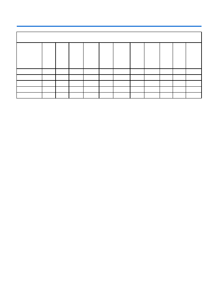
Table 2. MAX 7000B Speed Grades
Note (1)
Device
Speed Grade
-3
-4
-5
-7
-10
EPM7032B
v
v
v
EPM7064B
v
v
v
EPM7128B
v
v
v
EPM7256B
v
v
v
EPM7512B
v
v
v
4
Altera Corporation
MAX 7000B Programmable Logic Device Data Sheet
Notes:
(1)
When the IEEE Std. 1149.1 (JTAG) interface is used for in-system programming or boundary-scan testing, four I/O
pins become JTAG pins.
(2)
Contact Altera for up-to-date information on available device package options.
(3)
All 0.8-mm Ultra FineLine BGA packages are footprint-compatible via the SameFrame
TM
pin-out feature. Therefore,
designers can design a board to support a variety of devices, providing a flexible migration path across densities
and pin counts. Device migration is fully supported by Altera development tools. See
"SameFrame Pin-Outs" on
page 14
for more details.
(4)
All FineLine BGA packages are footprint-compatible via the SameFrame pin-out feature. Therefore, designers can
design a board to support a variety of devices, providing a flexible migration path across densities and pin counts.
Device migration is fully supported by Altera development tools. See
"SameFrame Pin-Outs" on page 14
for more
details.
MAX 7000B devices use CMOS EEPROM cells to implement logic
functions. The user-configurable MAX 7000B architecture accommodates
a variety of independent combinatorial and sequential logic functions.
The devices can be reprogrammed for quick and efficient iterations
during design development and debug cycles, and can be programmed
and erased up to 100 times.
MAX 7000B devices contain 32 to 512 macrocells that are combined into
groups of 16 macrocells, called logic array blocks (LABs). Each macrocell
has a programmable-
AND
/fixed-
OR
array and a configurable register with
independently programmable clock, clock enable, clear, and preset
functions. To build complex logic functions, each macrocell can be
supplemented with both shareable expander product terms and high-
speed parallel expander product terms to provide up to 32 product terms
per macrocell.
Table 3. MAX 7000B Maximum User I/O Pins
Note (1)
Device
44-Pin
PLCC
44-Pin
TQFP
48-Pin
TQFP
(2)
49-Pin
0.8-mm
Ultra
FineLine
BGA
(3)
100-
Pin
TQFP
100-Pin
FineLine
BGA
(4)
144-
Pin
TQFP
169-Pin
0.8-mm
Ultra
FineLine
BGA
(3)
208-
Pin
PQFP
256-
Pin
BGA
256-Pin
FineLine
BGA
(4)
EPM7032B
36
36
36
36
EPM7064B
36
36
40
41
68
68
EPM7128B
41
84
84
100
100
100
EPM7256B
84
120
141
164
164
EPM7512B
84
120
141
176
212
212

Altera Corporation
5
MAX 7000B Programmable Logic Device Data Sheet
MAX 7000B devices provide programmable speed/power optimization.
Speed-critical portions of a design can run at high speed/full power,
while the remaining portions run at reduced speed/low power. This
speed/power optimization feature enables the designer to configure one
or more macrocells to operate up to 50% lower power while adding only
a nominal timing delay. MAX 7000B devices also provide an option that
reduces the slew rate of the output buffers, minimizing noise transients
when non-speed-critical signals are switching. The output drivers of all
MAX 7000B devices can be set for 3.3 V, 2.5 V, or 1.8 V and all input pins
are 3.3-V, 2.5-V, and 1.8-V tolerant, allowing MAX 7000B devices to be
used in mixed-voltage systems.
MAX 7000B devices are supported by Altera development systems, which
are integrated packages that offer schematic, text--including VHDL,
Verilog HDL, and the Altera Hardware Description Language (AHDL)--
and waveform design entry, compilation and logic synthesis, simulation
and timing analysis, and device programming. Altera software provides
EDIF 2 0 0 and 3 0 0, LPM, VHDL, Verilog HDL, and other interfaces for
additional design entry and simulation support from other industry-
standard PC- and UNIX-workstation-based EDA tools. Altera software
runs on Windows-based PCs, as well as Sun SPARCstation, and HP 9000
Series 700/800 workstations.
f
For more information on development tools, see the
MAX+PLUS II
Programmable Logic Development System & Software Data Sheet
and the
Quartus Programmable Logic Development System & Software Data Sheet
.
Functional
Description
The MAX 7000B architecture includes the following elements:
LABs
Macrocells
Expander product terms (shareable and parallel)
PIA
I/O control blocks
The MAX 7000B architecture includes four dedicated inputs that can be
used as general-purpose inputs or as high-speed, global control signals
(clock, clear, and two output enable signals) for each macrocell and I/O
pin.
Figure 1
shows the architecture of MAX 7000B devices.