Document Outline
- MAX 9000 Programmable Logic Device Family Data Sheet
Æ
Altera Corporation
1
MAX 9000
Programmable Logic
Device Family
December 2002, ver. 6.4
Data Sheet
DS-M9000-6.4
Includes
MAX 9000A
Features...
High-performance CMOS EEPROM-based programmable logic
devices (PLDs) built on third-generation Multiple Array MatriX
(MAX
Æ
) architecture
5.0-V in-system programmability (ISP) through built-in IEEE Std.
1149.1 Joint Test Action Group (JTAG) interface
Built-in JTAG boundary-scan test (BST) circuitry compliant with IEEE
Std. 1149.1-1990
High-density erasable programmable logic device (EPLD) family
ranging from 6,000 to 12,000 usable gates (see
Table 1
)
10-ns pin-to-pin logic delays with counter frequencies of up to
144 MHz
Fully compliant with the peripheral component interconnect Special
Interest Group's (PCI SIG) PCI Local Bus Specification, Revision 2.2
Dual-output macrocell for independent use of combinatorial and
registered logic
FastTrack
Æ
Interconnect for fast, predictable interconnect delays
Input/output registers with clear and clock enable on all I/O pins
Programmable output slew-rate control to reduce switching noise
MultiVolt
TM
I/O interface operation, allowing devices to interface
with 3.3-V and 5.0-V devices
Configurable expander product-term distribution allowing up to 32
product terms per macrocell
Programmable power-saving mode for more than 50% power
reduction in each macrocell
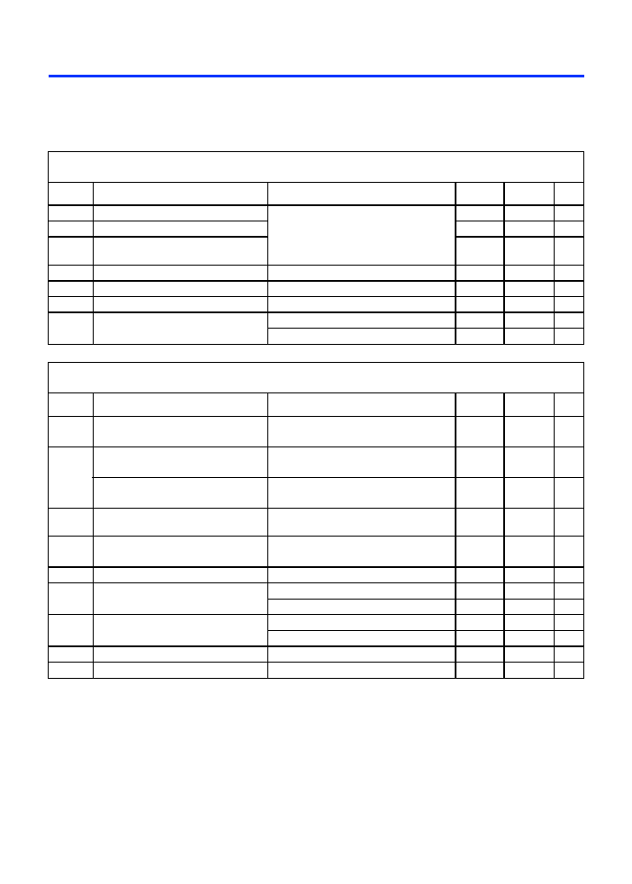
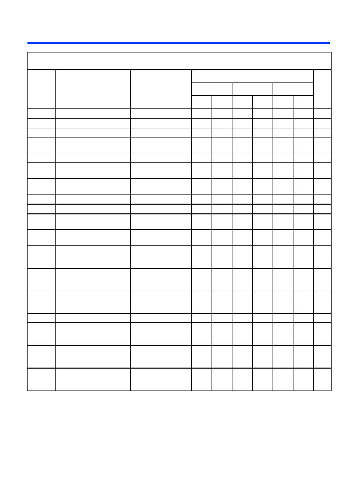
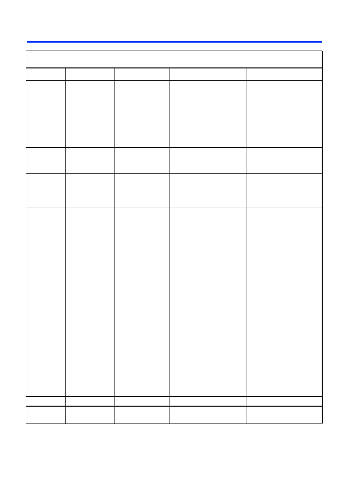
Table 1. MAX 9000 Device Features
Feature
EPM9320
EPM9320A
EPM9400
EPM9480
EPM9560
EPM9560A
Usable gates
6,000
8,000
10,000
12,000
Flipflops
484
580
676
772
Macrocells
320
400
480
560
Logic array blocks (LABs)
20
25
30
35
Maximum user I/O pins
168
159
175
216
t
PD1
(ns)
10
15
10
10
t
FSU
(ns)
3.0
5
3.0
3.0
t
FCO
(ns)
4.5
7
4.8
4.8
f
CNT
(MHz)
144
118
144
144
2
Altera Corporation
MAX 9000 Programmable Logic Device Family Data Sheet
...and More
Features
Programmable macrocell flipflops with individual clear, preset,
clock, and clock enable controls
Programmable security bit for protection of proprietary designs
Software design support and automatic place-and-route provided by
Altera's MAX+PLUS
Æ
II development system on Windows-based
PCs as well as Sun SPARCstation, HP 9000 Series 700/800, and IBM
RISC System/6000 workstations
Additional design entry and simulation support provided by EDIF
2 0 0 and 3 0 0 netlist files, library of parameterized modules (LPM),
Verilog HDL, VHDL, and other interfaces to popular EDA tools from
manufacturers such as Cadence, Exemplar Logic, Mentor Graphics,
OrCAD, Synopsys, Synplicity, and VeriBest
Programming support with Altera's Master Programming Unit
(MPU), BitBlaster
TM
serial download cable, ByteBlaster
TM
parallel
port download cable, and ByteBlasterMV
TM
parallel port download
cable, as well as programming hardware from third-party
manufacturers
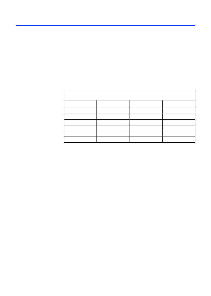
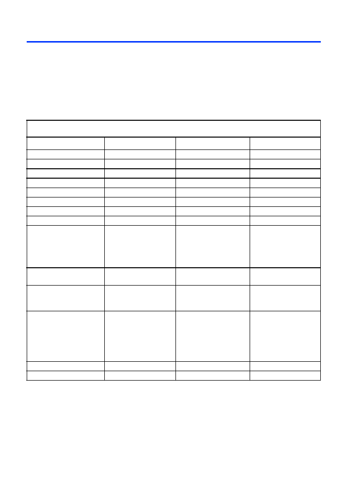
Offered in a variety of package options with 84 to 356 pins (see
Table 2
)
Notes:
(1)
MAX 9000 device package types include plastic J-lead chip carrier (PLCC), power
quad flat pack (RQFP), ceramic pin-grid array (PGA), and ball-grid array (BGA)
packages.
(2)
Perform a complete thermal analysis before committing a design to this device
package. See
Application Note 74 (Evaluating Power for Altera Devices)
.
Table 2. MAX 9000 Package Options & I/O Counts
Note (1)
Device
84-Pin
PLCC
208-Pin
RQFP
240-Pin
RQFP
280-Pin
PGA
304-Pin
RQFP
356-Pin
BGA
EPM9320
60
(2)
132
≠
168
≠
168
EPM9320A
60
(2)
132
≠
≠
≠
168
EPM9400
59
(2)
139
159
≠
≠
≠
EPM9480
≠
146
175
≠
≠
≠
EPM9560
≠
153 191
216
216
216
EPM9560A
≠
153 191
≠
≠
216
Altera Corporation
3
MAX 9000 Programmable Logic Device Family Data Sheet
General
Description
The MAX 9000 family of in-system-programmable, high-density, high-
performance EPLDs is based on Altera's third-generation MAX
architecture. Fabricated on an advanced CMOS technology, the EEPROM-
based MAX 9000 family provides 6,000 to 12,000 usable gates, pin-to-pin
delays as fast as 10 ns, and counter speeds of up to 144 MHz. The -10 speed
grade of the MAX 9000 family is compliant with the PCI Local Bus
Specification, Revision 2.2
.
Table 3
shows the speed grades available for
MAX 9000 devices.
Table 4
shows the performance of MAX 9000 devices for typical functions.
Note:
(1)
Internal logic array block (LAB) performance is shown. Numbers in parentheses show external delays from row
input pin to row I/O pin.
The MAX 9000 architecture supports high-density integration of system-
level logic functions. It easily integrates multiple programmable logic
devices ranging from PALs, GALs, and 22V10s to field-programmable
gate array (FPGA) devices and EPLDs.
Table 3. MAX 9000 Speed Grade Availability
Device
Speed Grade
-10
-15
-20
EPM9320
v
v
EPM9320A
v
EPM9400
v
v
EPM9480
v
v
EPM9560
v
v
EPM9560A
v
Table 4. MAX 9000 Performance
Note (1)
Application
Macrocells Used
Speed Grade
Units
-10
-15
-20
16-bit loadable counter
16
144
118
100
MHz
16-bit up/down counter
16
144
118
100
MHz
16-bit prescaled counter
16
144
118
100
MHz
16-bit address decode
1
5.6 (10)
7.9 (15)
10 (20)
ns
16-to-1 multiplexer
1
7.7 (12.1)
10.9 (18)
16 (26)
ns

4
Altera Corporation
MAX 9000 Programmable Logic Device Family Data Sheet
All MAX 9000 device packages provide four dedicated inputs for global
control signals with large fan-outs. Each I/O pin has an associated I/O
cell register with a clock enable control on the periphery of the device. As
outputs, these registers provide fast clock-to-output times; as inputs, they
offer quick setup times.
MAX 9000 EPLDs provide 5.0-V in-system programmability (ISP). This
feature allows the devices to be programmed and reprogrammed on the
printed circuit board (PCB) for quick and efficient iterations during design
development and debug cycles. MAX 9000 devices are guaranteed for 100
program and erase cycles.
MAX 9000 EPLDs contain 320 to 560 macrocells that are combined into
groups of 16 macrocells, called logic array blocks (LABs). Each macrocell
has a programmable-
AND
/fixed-
OR
array and a configurable register with
independently programmable clock, clock enable, clear, and preset
functions. For increased flexibility, each macrocell offers a dual-output
structure that allows the register and the product terms to be used
independently. This feature allows register-rich and combinatorial-
intensive designs to be implemented efficiently. The dual-output
structure of the MAX 9000 macrocell also improves logic utilization, thus
increasing the effective capacity of the devices. To build complex logic
functions, each macrocell can be supplemented with both shareable
expander product terms and high-speed parallel expander product terms
to provide up to 32 product terms per macrocell.
The MAX 9000 family provides programmable speed/power
optimization. Speed-critical portions of a design can run at high
speed/full power, while the remaining portions run at reduced
speed/low power. This speed/power optimization feature enables the
user to configure one or more macrocells to operate at 50% or less power
while adding only a nominal timing delay. MAX 9000 devices also
provide an option that reduces the slew rate of the output buffers,
minimizing noise transients when non-speed-critical signals are
switching. MAX 9000 devices offer the MultiVolt feature, which allows
output drivers to be set for either 3.3-V or 5.0-V operation in mixed-
voltage systems.

Altera Corporation
5
MAX 9000 Programmable Logic Device Family Data Sheet
The MAX 9000 family is supported by Altera's MAX+PLUS II
development system, a single, integrated software package that offers
schematic, text--including VHDL, Verilog HDL, and the Altera
Hardware Description Language (AHDL)--and waveform design entry,
compilation and logic synthesis, simulation and timing analysis, and
device programming. The MAX+PLUS II software provides EDIF 2 0 0
and 3 0 0, LPM, and other interfaces for additional design entry and
simulation support from other industry-standard PC- and UNIX-
workstation-based EDA tools. The MAX+PLUS II software runs on
Windows-based PCs as well as Sun SPARCstation, HP 9000 Series
700/800, and IBM RISC System/6000 workstations.
f
For more information on development tools, see the
MAX+PLUS II
Programmable Logic Development System & Software Data Sheet
.
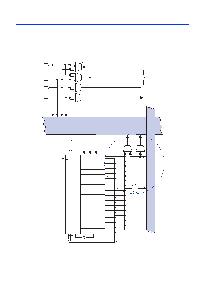
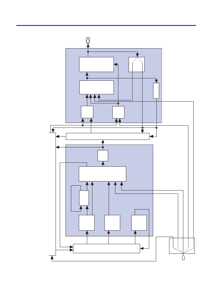
Functional
Description
MAX 9000 devices use a third-generation MAX architecture that yields
both high performance and a high degree of utilization for most
applications. The MAX 9000 architecture includes the following elements:
Logic array blocks
Macrocells
Expander product terms (shareable and parallel)
FastTrack Interconnect
Dedicated inputs
I/O cells
Figure 1
shows a block diagram of the MAX 9000 architecture.

6
Altera Corporation
MAX 9000 Programmable Logic Device Family Data Sheet
Figure 1. MAX 9000 Device Block Diagram
Logic Array Blocks
The MAX 9000 architecture is based on linking high-performance, flexible
logic array modules called logic array blocks (LABs). LABs consist of
16-macrocell arrays that are fed by the LAB local array, as shown in
Figure 2 on page 7
. Multiple LABs are linked together via the FastTrack
Interconnect, a series of fast, continuous channels that run the entire
length and width of the device. The I/O pins are supported by I/O cells
(IOCs) located at the end of each row (horizontal) and column (vertical)
path of the FastTrack Interconnect.
Each LAB is fed by 33 inputs from the row interconnect and 16 feedback
signals from the macrocells within the LAB. All of these signals are
available within the LAB in their true and inverted form. In addition,
16 shared expander product terms ("expanders") are available in their
inverted form, for a total of 114 signals that feed each product term in the
LAB. Each LAB is also fed by two low-skew global clocks and one global
clear that can be used for register control signals in all 16 macrocells.
IOC
IOC
IOC
IOC
IOC
IOC
IOC
IOC
IOC
IOC
IOC
IOC
IOC
IOC
I/O Cell
(IOC)
Logic Array
Block (LAB)
Macrocell
FastTrack
Interconnect
IOC
IOC
LAB Local Array
Altera Corporation
7
MAX 9000 Programmable Logic Device Family Data Sheet
LABs drive the row and column interconnect directly. Each macrocell can
drive out of the LAB onto one or both routing resources. Once on the row
or column interconnect, signals can traverse to other LABs or to the IOCs.
Figure 2. MAX 9000 Logic Array Block
Column FastTrack
Interconnect
Row FastTrack
Interconnect
33
48
To Peripheral Bus and
Other LABs in the Device
Global Control Select
DIN2
GCLR
16
16
48
See Figure 7
for details.
Macrocell 1
Macrocell 2
Macrocell 3
Macrocell 4
Macrocell 5
Macrocell 6
Macrocell 7
Macrocell 8
LAB Local Array
(114 Channels)
Shared Expander
Signals
Local Feedback
16
16
16
GCLK1
GCLK2
16
DIN3
DIN4
GOE
To Peripheral Bus
DIN1
Macrocell 9
Macrocell 10
Macrocell 11
Macrocell 12
Macrocell 13
Macrocell 14
Macrocell 15
Macrocell 16
8
Altera Corporation
MAX 9000 Programmable Logic Device Family Data Sheet
Macrocells
The MAX 9000 macrocell consists of three functional blocks: the product
terms, the product-term select matrix, and the programmable register.
The macrocell can be individually configured for both sequential and
combinatorial logic operation. See
Figure 3
.
Figure 3. MAX 9000 Macrocell & Local Array
Combinatorial logic is implemented in the local array, which provides five
product terms per macrocell. The product-term select matrix allocates
these product terms for use as either primary logic inputs (to the
OR
and
XOR
gates) to implement combinatorial functions, or as secondary inputs
to the macrocell's register clear, preset, clock, and clock enable control
functions. Two kinds of expander product terms ("expanders") are
available to supplement macrocell logic resources:
Shareable expanders, which are inverted product terms that are fed
back into the logic array
Parallel expanders, which are product terms borrowed from adjacent
macrocells
The MAX+PLUS II software automatically optimizes product-term
allocation according to the logic requirements of the design.
VCC
Product-
Term
Select
Matrix
16 Local
Feedbacks
16 Shareable
Expander Product
LAB Local
Array
Parallel
Expanders
(from Other
Macrocells)
Clear
Select
Global
Clear
Global
Clocks
Clock/
Enable
Select
2
PRN
CLRN
D/T
Q
ENA
Register
Bypass
To Row or
Column
FastTrack
Interconnect
Programmable
Register
Macrocell
Input Select
Local Array
Feedback
33 Row
FastTrack
Interconnect
Inputs

Altera Corporation
9
MAX 9000 Programmable Logic Device Family Data Sheet
For registered functions, each macrocell register can be individually
programmed for D, T, JK, or SR operation with programmable clock
control. The flipflop can also be bypassed for combinatorial operation.
During design entry, the user specifies the desired register type; the
MAX+PLUS II software then selects the most efficient register operation
for each registered function to optimize resource utilization.
Each programmable register can be clocked in three different modes:
By either global clock signal. This mode achieves the fastest clock-to-
output performance.
By a global clock signal and enabled by an active-high clock enable.
This mode provides an enable on each flipflop while still achieving
the fast clock-to-output performance of the global clock.
By an array clock implemented with a product term. In this mode, the
flipflop can be clocked by signals from buried macrocells or I/O pins.
Two global clock signals are available. As shown in
Figure 2
, these global
clock signals can be the true or the complement of either of the global clock
pins (
DIN1
and
DIN2
).
Each register also supports asynchronous preset and clear functions. As
shown in
Figure 3
, the product-term select matrix allocates product terms
to control these operations. Although the product-term-driven preset and
clear inputs to registers are active high, active-low control can be obtained
by inverting the signal within the logic array. In addition, each register
clear function can be individually driven by the dedicated global clear pin
(
DIN3
). The global clear can be programmed for active-high or active-low
operation.
All MAX 9000 macrocells offer a dual-output structure that provides
independent register and combinatorial logic output within the same
macrocell. This function is implemented by a process called register
packing. When register packing is used, the product-term select matrix
allocates one product term to the D input of the register, while the
remaining product terms can be used to implement unrelated
combinatorial logic. Both the registered and the combinatorial output of
the macrocell can feed either the FastTrack Interconnect or the LAB local
array.
10
Altera Corporation
MAX 9000 Programmable Logic Device Family Data Sheet
Expander Product Terms
Although most logic functions can be implemented with the five product
terms available in each macrocell, some logic functions are more complex
and require additional product terms. Although another macrocell can
supply the required logic resources, the MAX 9000 architecture also offers
both shareable and parallel expander product terms that provide
additional product terms directly to any macrocell in the same LAB. These
expanders help ensure that logic is synthesized with the fewest possible
logic resources to obtain the fastest possible speed.
Shareable Expanders
Each LAB has 16 shareable expanders that can be viewed as a pool of
uncommitted single product terms (one from each macrocell) with
inverted outputs that feed back into the LAB local array. Each shareable
expander can be used and shared by any or all macrocells in the LAB to
build complex logic functions. A small delay (t
LOCAL
+ t
SEXP
) is incurred
when shareable expanders are used.
Figure 4
shows how shareable
expanders can feed multiple macrocells.
Figure 4. MAX 9000 Shareable Expanders
Macrocell
Product-Term
Logic
Product-Term Select Matrix
Macrocell
Product-Term
Logic
LAB Local Array
16 Local
Feedbacks
16 Shared
Expanders
33 Row
FastTrack
Interconnect
Signals
Shareable expanders can be shared by any or all macrocells in the LAB.
Altera Corporation
11
MAX 9000 Programmable Logic Device Family Data Sheet
Parallel Expanders
Parallel expanders are unused product terms that can be allocated to a
neighboring macrocell to implement fast, complex logic functions.
Parallel expanders allow up to 20 product terms to directly feed the
macrocell
OR
logic, with five product terms provided by the macrocell and
15 parallel expanders provided by neighboring macrocells in the LAB.
Figure 5
shows how parallel expanders can feed the neighboring
macrocell.
Figure 5. MAX 9000 Parallel Expanders
Preset
Clock
Clear
Product-
Term
Select
Matrix
Preset
Clock
Clear
Product-
Term
Select
Matrix
Macrocell
Product-
Term Logic
From
Previous
Macrocell
To Next
Macrocell
LAB Local
Array
Macrocell
Product-
Term Logic
33 Row
FastTrack
Interconnect
Signals
16 Local
Feedbacks
16 Shared
Expanders
Unused product terms in a macrocell can be allocated to a neighboring macrocell.

12
Altera Corporation
MAX 9000 Programmable Logic Device Family Data Sheet
The MAX+PLUS II Compiler automatically allocates as many as three sets
of up to five parallel expanders to macrocells that require additional
product terms. Each set of expanders incurs a small, incremental timing
delay (t
PEXP
). For example, if a macrocell requires 14 product terms, the
Compiler uses the five dedicated product terms within the macrocell and
allocates two sets of parallel expanders; the first set includes five product
terms and the second set includes four product terms, increasing the total
delay by 2
◊
t
PEXP
.
Two groups of eight macrocells within each LAB (e.g., macrocells 1
through 8 and 9 through 16) form two chains to lend or borrow parallel
expanders. A macrocell borrows parallel expanders from lower-
numbered macrocells. For example, macrocell 8 can borrow parallel
expanders from macrocell 7, from macrocells 7 and 6, or from macrocells
7, 6, and 5. Within each group of 8, the lowest-numbered macrocell can
only lend parallel expanders and the highest-numbered macrocell can
only borrow them.
FastTrack Interconnect
In the MAX 9000 architecture, connections between macrocells and device
I/O pins are provided by the FastTrack Interconnect, a series of
continuous horizontal and vertical routing channels that traverse the
entire device. This device-wide routing structure provides predictable
performance even in complex designs. In contrast, the segmented routing
in FPGAs requires switch matrices to connect a variable number of
routing paths, increasing the delays between logic resources and reducing
performance.
Figure 6
shows the interconnection of four adjacent LABs
with row and column interconnects.
Altera Corporation
13
MAX 9000 Programmable Logic Device Family Data Sheet
Figure 6. MAX 9000 Device Interconnect Resources
The LABs within MAX 9000 devices are arranged into a matrix of columns
and rows.
Table 5
shows the number of columns and rows in each
MAX 9000 device.
Each LAB is named on the basis of its physical row (A, B, C, etc.) and column (1, 2, 3, etc.) position within the device.
LAB
A1
LAB
A2
LAB
B1
LAB
B2
Column
FastTrack
Interconnect
Row FastTrack
Interconnect
See Figure 8
for details.
See Figure 9
for details.
IOC1
IOC10
IOC1
IOC10
IOC1
IOC8
IOC1
IOC8
IOC1
IOC10
IOC1
IOC10
IOC1
IOC8
IOC1
IOC8
See Figure 7
for details.
Table 5. MAX 9000 Rows & Columns
Devices
Rows
Columns
EPM9320, EPM9320A
4
5
EPM9400
5
5
EPM9480
6
5
EPM9560, EPM9560A
7
5

14
Altera Corporation
MAX 9000 Programmable Logic Device Family Data Sheet
Each row of LABs has a dedicated row interconnect that routes signals
both into and out of the LABs in the row. The row interconnect can then
drive I/O pins or feed other LABs in the device. Each row interconnect has
a total of 96 channels.
Figure 7
shows how a macrocell drives the row and
column interconnect.
Figure 7. MAX 9000 LAB Connections to Row & Column Interconnect
Each macrocell in the LAB can drive one of three separate column
interconnect channels. The column channels run vertically across the
entire device, and are shared by the macrocells in the same column. The
MAX+PLUS II Compiler optimizes connections to a column channel
automatically.
Macrocell 1
Macrocell 2
96 Row Channels
48 Column
Channels
Each macrocell drives one
of three column channels.
To LAB
Local Array
Each macrocell drives
one row channel.
Additional multiplexer provides
column-to-row path if
macrocell drives row channel.
Dual-output
macrocell feeds
both FastTrack
Interconnect and
LAB local array.
LAB
Altera Corporation
15
MAX 9000 Programmable Logic Device Family Data Sheet
A row interconnect channel can be fed by the output of the macrocell
through a 4-to-1 multiplexer that the macrocell shares with three column
channels. If the multiplexer is used for a macrocell-to-row connection, the
three column signals can access another row channel via an additional
3-to-1 multiplexer. Within any LAB, the multiplexers provide all
48 column channels with access to 32 row channels.
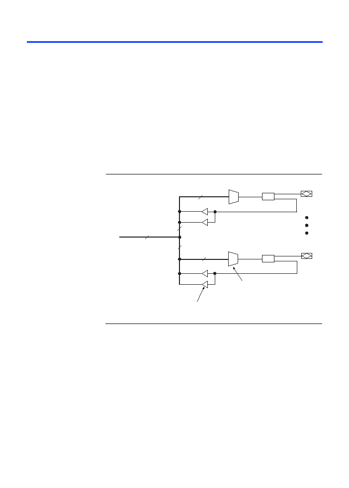
Row-to-I/O Cell Connections
Figure 8
illustrates the connections between row interconnect channels
and IOCs. An input signal from an IOC can drive two separate row
channels. When an IOC is used as an output, the signal is driven by a
10-to-1 multiplexer that selects the row channels. Each end of the row
channel feeds up to eight IOCs on the periphery of the device.
Figure 8. MAX 9000 Row-to-IOC Connections
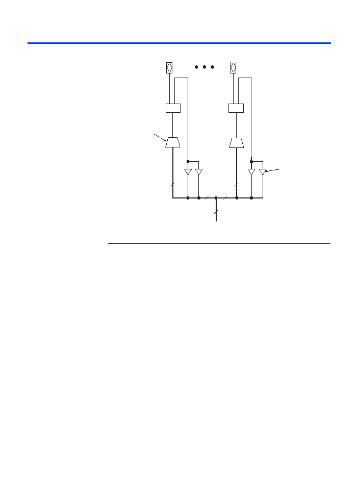
Column-to-I/O Cell Connections
Each end of a column channel has up to 10 IOCs (see
Figure 9
). An input
signal from an IOC can drive two separate column channels. When an IOC
is used as an output, the signal is driven by a 17-to-1 multiplexer that
selects the column channels.
96
96
Each IOC is driven by
a 10-to-1 multiplexer.
Each IOC can drive up to
two row channels.
IOC8
IOC1
10
10
Row FastTrack
Interconnect
96
16
Altera Corporation
MAX 9000 Programmable Logic Device Family Data Sheet
Figure 9. MAX 9000 Column-to-IOC Connections
Dedicated Inputs
In addition to the general-purpose I/O pins, MAX 9000 devices have four
dedicated input pins. These dedicated inputs provide low-skew, device-
wide signal distribution to the LABs and IOCs in the device, and are
typically used for global clock, clear, and output enable control signals.
The global control signals can feed the macrocell or IOC clock and clear
inputs, as well as the IOC output enable. The dedicated inputs can also be
used as general-purpose data inputs because they can feed the row
FastTrack Interconnect (see
Figure 2 on page 7
).
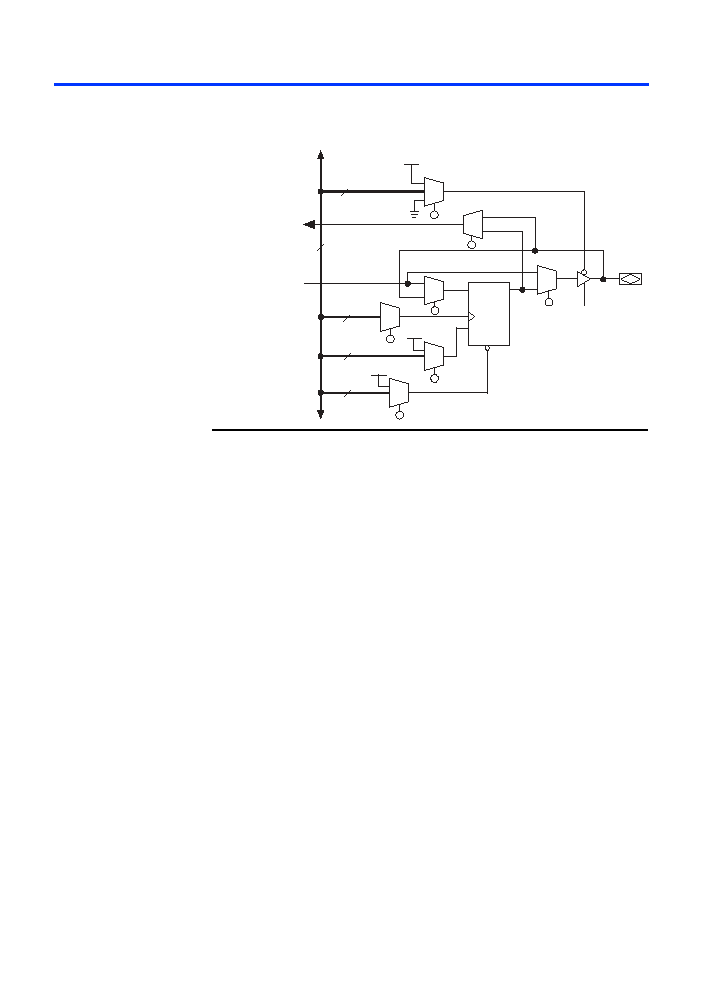
I/O Cells
Figure 10
shows the IOC block diagram. Signals enter the MAX 9000
device from either the I/O pins that provide general-purpose input
capability or from the four dedicated inputs. The IOCs are located at the
ends of the row and column interconnect channels.
48
Each IOC is driven by
a 17-to-1 multiplexer.
Each IOC can drive up
to two column
channels.
17
17
Column FastTrack
Interconnect
IOC10
IOC1
48
48
Altera Corporation
17
MAX 9000 Programmable Logic Device Family Data Sheet
Figure 10. MAX 9000 IOC
I/O pins can be used as input, output, or bidirectional pins. Each IOC has
an IOC register with a clock enable input. This register can be used either
as an input register for external data that requires fast setup times, or as an
output register for data that requires fast clock-to-output performance.
The IOC register clock enable allows the global clock to be used for fast
clock-to-output performance, while maintaining the flexibility required
for selective clocking.
The clock, clock enable, clear, and output enable controls for the IOCs are
provided by a network of I/O control signals. These signals can be
supplied by either the dedicated input pins or internal logic. The IOC
control-signal paths are designed to minimize the skew across the device.
All control-signal sources are buffered onto high-speed drivers that drive
the signals around the periphery of the device. This "peripheral bus" can
be configured to provide up to eight output enable signals, up to four
clock signals, up to six clock enable signals, and up to two clear signals.
Table 6 on page 18
shows the sources that drive the peripheral bus and
how the IOC control signals share the peripheral bus.
Slew-Rate
Control
From Row or
Column FastTrack
Interconnect
4
2
8
13
To Row or
Column FastTrack
Interconnect
OE [7..0]
CLK [3..0]
ENA [5..0]
CLR [1..0]
Peripheral Control
Bus [12..0]
CLRN
D
Q
ENA
VCC
VCC
6
VCC

18
Altera Corporation
MAX 9000 Programmable Logic Device Family Data Sheet
The output buffer in each IOC has an adjustable output slew rate that can
be configured for low-noise or high-speed performance. A slower slew
rate reduces board-level noise and adds a nominal timing delay to the
output buffer delay (t
OD
) parameter. The fast slew rate should be used for
speed-critical outputs in systems that are adequately protected against
noise. Designers can specify the slew rate on a pin-by-pin basis during
design entry or assign a default slew rate to all pins on a global basis. The
slew rate control affects both rising and falling edges of the output signals.
Output
Configuration
The MAX 9000 device architecture supports the MultiVolt I/O interface
feature, which allows MAX 9000 devices to interface with systems of
differing supply voltages. The 5.0-V devices in all packages can be set for
3.3-V or 5.0-V I/O pin operation. These devices have one set of V
CC
pins
for internal operation and input buffers (
VCCINT
), and another set for I/O
output drivers (
VCCIO
).
The
VCCINT
pins must always be connected to a 5.0-V power supply.
With a 5.0-V V
CCINT
level, input voltages are at TTL levels and are
therefore compatible with 3.3-V and 5.0-V inputs.
Table 6. Peripheral Bus Sources
Peripheral Control
Signal
Source
EPM9320
EPM9320A
EPM9400
EPM9480
EPM9560
EPM9560A
OE0/ENA0
Row C
Row E
Row F
Row G
OE1/ENA1
Row B
Row E
Row F
Row F
OE2/ENA2
Row A
Row E
Row E
Row E
OE3/ENA3
Row B
Row B
Row B
Row B
OE4/ENA4
Row A
Row A
Row A
Row A
OE5
Row D
Row D
Row D
Row D
OE6
Row C
Row C
Row C
Row C
OE7/CLR1
Row B/
GOE
Row B/
GOE
Row B/
GOE
Row B/
GOE
CLR0/ENA5
Row A/
GCLR
Row A/
GCLR
Row A/
GCLR
Row A/
GCLR
CLK0
GCLK1
GCLK1
GCLK1
GCLK1
CLK1
GCLK2
GCLK2
GCLK2
GCLK2
CLK2
Row D
Row D
Row D
Row D
CLK3
Row C
Row C
Row C
Row C

Altera Corporation
19
MAX 9000 Programmable Logic Device Family Data Sheet
The
VCCIO
pins can be connected to either a 3.3-V or 5.0-V power supply,
depending on the output requirements. When the
VCCIO
pins are
connected to a 5.0-V power supply, the output levels are compatible with
5.0-V systems. When the
VCCIO
pins are connected to a 3.3-V power
supply, the output high is at 3.3 V and is therefore compatible with 3.3-V
or 5.0-V systems. Devices operating with V
CCIO
levels lower than 4.75 V
incur a nominally greater timing delay of t
OD2
instead of t
OD1
.
In-System
Programma-
bility (ISP)
MAX 9000 devices can be programmed in-system through a 4-pin JTAG
interface. ISP offers quick and efficient iterations during design
development and debug cycles. The MAX 9000 architecture internally
generates the 12.0-V programming voltage required to program EEPROM
cells, eliminating the need for an external 12.0-V power supply to
program the devices on the board. During ISP, the I/O pins are tri-stated
to eliminate board conflicts.
ISP simplifies the manufacturing flow by allowing the devices to be
mounted on a printed circuit board with standard pick-and-place
equipment before they are programmed. MAX 9000 devices can be
programmed by downloading the information via in-circuit testers,
embedded processors, or the Altera BitBlaster, ByteBlaster, or
ByteBlasterMV download cable. (The ByteBlaster cable is obsolete and has
been replaced by the ByteBlasterMV cable, which can interface with 2.5-V,
3.3-V, and 5.0-V devices.) Programming the devices after they are placed
on the board eliminates lead damage on high pin-count packages (e.g.,
QFP packages) due to device handling. MAX 9000 devices can also be
reprogrammed in the field (i.e., product upgrades can be performed in the
field via software or modem).
In-system programming can be accomplished with either an adaptive or
constant algorithm. An adaptive algorithm reads information from the
unit and adapts subsequent programming steps to achieve the fastest
possible programming time for that unit. Because some in-circuit testers
platforms have difficulties supporting an adaptive algorithm, Altera
offers devices tested with a constant algorithm. Devices tested to the
constant algorithm have an "F" suffix in the ordering code.
Programming
with External
Hardware
MAX 9000 devices can be programmed on Windows-based PCs with an
Altera Logic Programmer card, the Master Programming Unit (MPU),
and the appropriate device adapter. The MPU performs continuity
checking to ensure adequate electrical contact between the adapter and
the device.
f
For more information, see the
Altera Programming Hardware Data Sheet
.
20
Altera Corporation
MAX 9000 Programmable Logic Device Family Data Sheet
The MAX+PLUS II software can use text- or waveform-format test vectors
created with the MAX+PLUS II Text Editor or Waveform Editor to test a
programmed device. For added design verification, designers can
perform functional testing to compare the functional behavior of a
MAX 9000 device with the results of simulation.
Data I/O, BP Microsystems, and other programming hardware
manufacturers also provide programming support for Altera devices.
f
For more information, see
Programming Hardware Manufacturers.
IEEE Std.
1149.1 (JTAG)
Boundary-Scan
Support
MAX 9000 devices support JTAG BST circuitry as specified by IEEE Std.
1149.1-1990.
Table 7
describes the JTAG instructions supported by the
MAX 9000 family. The pin-out tables starting on
page 35
show the
location of the JTAG control pins for each device. If the JTAG interface is
not required, the JTAG pins are available as user I/O pins.
Table 7. MAX 9000 JTAG Instructions
JTAG Instruction
Description
SAMPLE/PRELOAD Allows a snapshot of signals at the device pins to be captured and examined during
normal device operation, and permits an initial data pattern output at the device pins.
EXTEST
Allows the external circuitry and board-level interconnections to be tested by forcing a test
pattern at the output pins and capturing test results at the input pins.
BYPASS
Places the 1-bit bypass register between the
TDI
and
TDO
pins, which allows the BST
data to pass synchronously through a selected device to adjacent devices during normal
device operation.
IDCODE
Selects the IDCODE register and places it between
TDI
and
TDO
, allowing the IDCODE
to be shifted out of
TDO
. Supported by the EPM9320A, EPM9400, EPM9480, and
EPM9560A devices only.
UESCODE
Selects the user electronic signature (UESCODE) register and allows the UESCODE to
be shifted out of
TDO
serially. This instruction is supported by MAX 9000A devices only.
ISP Instructions
These instructions are used when programming MAX 9000 devices via the JTAG ports
with the BitBlaster or ByteBlasterMV download cable, or using a Jam File (.jam), Jam
Byte-Code File (.jbc), or Serial Vector Format (.svf) File via an embedded processor or
test equipment.

Altera Corporation
21
MAX 9000 Programmable Logic Device Family Data Sheet
The instruction register length for MAX 9000 devices is 10 bits. EPM9320A
and EPM9560A devices support a 16-bit UESCODE register.
Tables 8
and
9
show the boundary-scan register length and device IDCODE
information for MAX 9000 devices.
Notes:
(1)
The IDCODE's least significant bit (LSB) is always
1
.
(2)
The most significant bit (MSB) is on the left.
(3)
Although the EPM9320A and EPM9560A devices support the IDCODE instruction,
the EPM9320 and EPM9560 devices do not.
Figure 11
shows the timing requirements for the JTAG signals.
Table 8. MAX 9000 Boundary-Scan Register Length
Device
Boundary-Scan Register Length
EPM9320, EPM9320A
504
EPM9400
552
EPM9480
600
EPM9560, EPM9560A
648
Table 9. 32-Bit MAX 9000 Device IDCODE
Note (1)
Device
IDCODE (32 Bits)
Version
(4 Bits)
Part Number
(16 Bits)
(2)
Manufacturer's
Identity (11 Bits)
1
(1 Bit)
EPM9320A
(3)
0000
1001 0011 0010 0000
00001101110
1
EPM9400
0000
1001 0100 0000 0000
00001101110
1
EPM9480
0000
1001 0100 1000 0000
00001101110
1
EPM9560A
(3)
0000
1001 0101 0110 0000
00001101110
1

22
Altera Corporation
MAX 9000 Programmable Logic Device Family Data Sheet
Figure 11. MAX 9000 JTAG Waveforms
Table 10
shows the JTAG timing parameters and values for MAX 9000
devices.
f
For detailed information on JTAG operation in MAX 9000 devices, refer to
Application Note 39 (IEEE 1149.1 (JTAG) Boundary-Scan Testing in Altera
Devices)
.
Table 10. JTAG Timing Parameters & Values for MAX 9000 Devices
Symbol
Parameter
Min
Max
Unit
t
JCP
TCK
clock period
100
ns
t
JCH
TCK
clock high time
50
ns
t
JCL
TCK
clock low time
50
ns
t
JPSU
JTAG port setup time
20
ns
t
JPH
JTAG port hold time
45
ns
t
JPCO
JTAG port clock to output
25
ns
t
JPZX
JTAG port high impedance to valid output
25
ns
t
JPXZ
JTAG port valid output to high impedance
25
ns
t
JSSU
Capture register setup time
20
ns
t
JSH
Capture register hold time
45
ns
t
JSCO
Update register clock to output
25
ns
t
JSZX
Update register high impedance to valid output
25
ns
t
JSXZ
Update register valid output to high impedance
25
ns
TDO
TCK
t
JPZX
t
JPCO
t
JPH
t
JPXZ
t
JCP
t
JPSU
t
JCL
t
JCH
TDI
TMS
Signal
to Be
Captured
Signal
to Be
Driven
t
JSZX
t
JSSU
t
JSH
t
JSCO
t
JSXZ

Altera Corporation
23
MAX 9000 Programmable Logic Device Family Data Sheet
Programmable
Speed/Power
Control
MAX 9000 devices offer a power-saving mode that supports low-power
operation across user-defined signal paths or the entire device. Because
most logic applications require only a small fraction of all gates to operate
at maximum frequency, this feature allows total power dissipation to be
reduced by 50% or more.
The designer can program each individual macrocell in a MAX 9000
device for either high-speed (i.e., with the Turbo Bit
TM
option turned on) or
low-power (i.e., with the Turbo Bit option turned off) operation. As a
result, speed-critical paths in the design can run at high speed, while
remaining paths operate at reduced power. Macrocells that run at low
power incur a nominal timing delay adder (t
LPA
) for the LAB local array
delay (t
LOCAL
).
Design Security
All MAX 9000 EPLDs contain a programmable security bit that controls
access to the data programmed into the device. When this bit is
programmed, a proprietary design implemented in the device cannot be
copied or retrieved. This feature provides a high level of design security,
because programmed data within EEPROM cells is invisible. The security
bit that controls this function, as well as all other programmed data, is
reset only when the device is erased.
Generic Testing
MAX 9000 EPLDs are fully functionally tested. Complete testing of each
programmable EEPROM bit and all logic functionality ensures 100%
programming yield. AC test measurements are taken under conditions
equivalent to those shown in
Figure 12
. Test patterns can be used and then
erased during the early stages of the production flow.
Figure 12. MAX 9000 AC Test Conditions
VCC
To Test
System
C1 (includes
JIG capacitance)
Device input
rise and fall
times < 3 ns
Device
Output
464
(703
)
250
(8.06 K
)
Power supply transients can affect AC
measurements. Simultaneous transitions of
multiple outputs should be avoided for
accurate measurement. Threshold tests
must not be performed under AC
conditions. Large-amplitude, fast ground-
current transients normally occur as the
device outputs discharge the load
capacitances. When these transients flow
through the parasitic inductance between
the device ground pin and the test system
ground, significant reductions in
observable noise immunity can result.
Numbers in parentheses are for 3.3-V
outputs. Numbers without parentheses are
for 5.0-V devices or outputs.
24
Altera Corporation
MAX 9000 Programmable Logic Device Family Data Sheet
Operating
Conditions
Tables 11
through
17
provide information on absolute maximum ratings,
recommended operating conditions, operating conditions, and
capacitance for MAX 9000 devices.
Table 11. MAX 9000 Device Absolute Maximum Ratings
Note (1)
Symbol
Parameter
Conditions
Min
Max
Unit
V
CC
Supply voltage
With respect to ground
(2)
≠2.0
7.0
V
V
I
DC input voltage
≠2.0
7.0
V
V
CCISP
Supply voltage during in-system
programming
≠2.0
7.0
V
I
OUT
DC output current, per pin
≠25
25
mA
T
STG
Storage temperature
No bias
≠65
150
∞
C
T
AMB
Ambient temperature
Under bias
≠65
135
∞
C
T
J
Junction temperature
Ceramic packages, under bias
150
∞
C
PQFP and RQFP packages, under bias
135
∞
C
Table 12. MAX 9000 Device Recommended Operating Conditions
Symbol
Parameter
Conditions
Min
Max
Unit
V
CCINT
Supply voltage for internal logic and
input buffers
(3)
,
(4)
4.75
(4.50)
5.25
(5.50)
V
V
CCI O
Supply voltage for output drivers,
5.0-V operation
(3)
,
(4)
4.75
(4.50)
5.25
(5.50)
V
Supply voltage for output drivers,
3.3-V operation
(3)
,
(4)
3.00
(3.00)
3.60
(3.60)
V
V
CCISP
Supply voltage during in-system
programming
4.75
5.25
V
V
I
Input voltage
≠0.5
V
CCINT
+
0.5
V
V
O
Output voltage
0
V
CCIO
V
T
A
Ambient temperature
For commercial use
0
70
∞
C
For industrial use
≠40
85
∞
C
T
J
Junction temperature
For commercial use
0
90
∞
C
For industrial use
≠40
105
∞
C
t
R
Input rise time
40
ns
t
F
Input fall time
40
ns

Altera Corporation
25
MAX 9000 Programmable Logic Device Family Data Sheet
Table 13. MAX 9000 Device DC Operating Conditions
Notes (5)
,
(6)
Symbol
Parameter
Conditions
Min
Max
Unit
V
IH
High-level input voltage
(7)
2.0
V
CCINT
+
0.5
V
V
IL
Low-level input voltage
≠0.5
0.8
V
V
OH
5.0-V high-level TTL output voltage
I
OH
= ≠4 mA DC, V
CCIO
= 4.75 V
(8)
2.4
V
3.3-V high-level TTL output voltage
I
OH
= ≠4 mA DC, V
CCIO
= 3.00 V
(8)
2.4
V
3.3-V high-level CMOS output voltage
I
OH
= ≠0.1 mA DC, V
CCIO
= 3.00 V
(8)
V
CCIO
≠
0.2
V
V
OL
5.0-V low level TTL output voltage
I
OL
= 12 mA DC, V
CCIO
= 4.75 V
(8)
0.45
V
3.3-V low-level TTL output voltage
I
OL
= 12 mA DC, V
CCIO
= 3.00 V
(8)
0.45
V
3.3-V low-level CMOS output voltage
I
OL
= 0.1 mA DC, V
CCIO
= 3.00 V
(8)
0.2
V
I
I
I/O pin leakage current of dedicated input
pins
V
I
= ≠0.5 to 5.5 V
(9)
≠10
10
µ
A
I
OZ
Tri-state output off-state current
V
I
= ≠0.5 to 5.5 V
≠40
40
µ
A
Table 14. MAX 9000 Device Capacitance: EPM9320, EPM9400, EPM9480 & EPM9560 Devices
Note (10)
Symbol
Parameter
Conditions
Min
Max
Unit
C
DIN1
Dedicated input capacitance
V
IN
= 0 V, f = 1.0 MHz
18
pF
C
DIN2
Dedicated input capacitance
V
IN
= 0 V, f = 1.0 MHz
18
pF
C
DIN3
Dedicated input capacitance
V
IN
= 0 V, f = 1.0 MHz
17
pF
C
DIN4
Dedicated input capacitance
V
IN
= 0 V, f = 1.0 MHz
20
pF
C
I/O
I/O pin capacitance
V
IN
= 0 V, f = 1.0 MHz
12
pF
Table 15. MAX 9000A Device Capacitance: EPM9320A & EPM9560A Devices
Note (10)
Symbol
Parameter
Conditions
Min
Max
Unit
C
DIN1
Dedicated input capacitance
V
IN
= 0 V, f = 1.0 MHz
16
pF
C
DIN2
Dedicated input capacitance
V
IN
= 0 V, f = 1.0 MHz
10
pF
C
DIN3
Dedicated input capacitance
V
IN
= 0 V, f = 1.0 MHz
10
pF
C
DIN4
Dedicated input capacitance
V
IN
= 0 V, f = 1.0 MHz
12
pF
C
I/O
I/O pin capacitance
V
IN
= 0 V, f = 1.0 MHz
8
pF
Table 16. MAX 9000 Device Typical I
CC
Supply Current Values
Symbol
Parameter
Conditions
EPM9320 EPM9400 EPM9480 EPM9560 Unit
I
CC1
I
CC
supply current (low-power
mode, standby, typical)
V
I
= ground,
no load
(11)
106
132
140
146
mA
26
Altera Corporation
MAX 9000 Programmable Logic Device Family Data Sheet
Notes to tables:
(1)
See the
Operating Requirements for Altera Devices Data Sheet
.
(2)
Minimum DC input on I/O pins is ≠0.5 V and on the four dedicated input pins is ≠0.3 V. During transitions, the
inputs may undershoot to ≠2.0 V or overshoot to 7.0 V for periods shorter than 20 ns under no-load conditions.
(3)
V
CC
must rise monotonically.
(4)
Numbers in parentheses are for industrial-temperature-range devices.
(5)
Typical values are for T
A
= 25
∞
C and V
CC
= 5.0 V.
(6)
These values are specified under the MAX 9000 recommended operating conditions, shown in
Table 12 on page 24
.
(7)
During in-system programming, the minimum V
IH
of the JTAG
TCK
pin is 3.6 V. The minimum V
IH
of this pin
during JTAG testing remains at 2.0 V. To attain this 3.6-V V
IH
during programming, the ByteBlaster and
ByteBlasterMV download cables must have a 5.0-V V
CC
.
(8)
This parameter is measured with 50% of the outputs each sinking 12 mA. The I
OH
parameter refers to high-level
TTL or CMOS output current; the I
OL
parameter refers to the low-level TTL or CMOS output current.
(9)
JTAG pin input leakage is typically ≠60
µ
.
(10) Capacitance is sample-tested only and is measured at 25
∞
C.
(11) Measured with a 16-bit loadable, enabled, up/down counter programmed into each LAB. I
CC
is measured at 0
∞
C.
Figure 13
shows typical output drive characteristics for MAX 9000 devices
with 5.0-V and 3.3-V V
CCIO
.
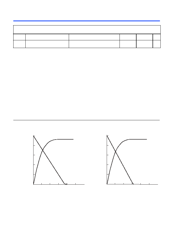
Figure 13. Output Drive Characteristics of MAX 9000 Devices
Note (1)
Note:
(1)
Output drive characteristics include the JTAG
TDO
pin.
Table 17. MAX 9000A Device Typical I
CC
Supply Current Values
Symbol
Parameter
Conditions
EPM9320A EPM9560A Unit
I
CC1
I
CC
supply current (low-power
mode, standby, typical)
V
I
= ground, no load
(11)
99
174
mA
1
2
3
4
5
30
60
90
150
120
V
CCIO
= 5.0 V
I
OL
I
OH
Room Temperature
1
2
3
4
5
30
60
90
150
120
V
CCIO
= 3.3 V
I
OL
I
OH
Room Temperature
3.3
Typical I
Output
Current (mA)
Output Voltage (V)
Output Voltage (V)
O
Typical I
Output
Current (mA)
O
5.0-V
3.3-V

Altera Corporation
27
MAX 9000 Programmable Logic Device Family Data Sheet
Timing Model
The continuous, high-performance FastTrack Interconnect ensures
predictable performance and accurate simulation and timing analysis.
This predictable performance contrasts with that of FPGAs, which use a
segmented connection scheme and hence have unpredictable
performance. Timing simulation and delay prediction are available with
the MAX+PLUS II Simulator and Timing Analyzer, or with industry-
standard EDA tools. The Simulator offers both pre-synthesis functional
simulation to evaluate logic design accuracy and post-synthesis timing
simulation with 0.1-ns resolution. The Timing Analyzer provides point-
to-point timing delay information, setup and hold time prediction, and
device-wide performance analysis.
The MAX 9000 timing model in
Figure 14
shows the delays that
correspond to various paths and functions in the circuit. This model
contains three distinct parts: the macrocell, IOC, and interconnect,
including the row and column FastTrack Interconnect and LAB local array
paths. Each parameter shown in
Figure 14
is expressed as a worst-case
value in the internal timing characteristics tables in this data sheet. Hand-
calculations that use the MAX 9000 timing model and these timing
parameters can be used to estimate MAX 9000 device performance.
f
For more information on calculating MAX 9000 timing delays, see
Application Note 77 (Understanding MAX 9000 Timing)
.
28
Altera Corporation
MAX 9000 Programmable Logic Device Family Data Sheet
Figure 14. MAX 9000 Timing Model
Macrocell
t
RD
t
COMB
t
SU
t
H
t
PRE
t
CLR
Macrocell/
Register
Delays
Logic Array
Delay
t
LAD
Register
Control Delay
Shared Expander
Delay
t
SEXP
Global Input
Delays
I/O Pi
n
t
INREG
t
IODR
t
IODC
I/O Register
Delays
Output Data
Delay
I/O Cell
Control Delay
Input
Delay
Output
Delays
t
IORD
t
IOCOMB
t
IOSU
t
IOH
t
IOCLR
t
OD1
t
OD2
t
OD3
t
XZ
t
ZX1
t
ZX2
t
ZX3
IOC
t
COL
t
ROW
t
LOCAL
Parallel Expander
Delay
t
PEXP
t
DIN_D
t
DIN_CLK
t
DIN_CLR
t
DIN_IO
t
DIN_IOC
FastT
rack
Drive Delay
t
INCOMB
I/O Register
Feedback Delay
t
IOFD
t
LAC
t
IC
t
EN
t
FTD
t
IOC

Altera Corporation
29
MAX 9000 Programmable Logic Device Family Data Sheet
Tables 18
through
21
show timing for MAX 9000 devices.
Table 18. MAX 9000 External Timing Characteristics
Note (1)
Symbol
Parameter
Conditions
Speed Grade
Unit
-10
-15
-20
Min
Max
Min
Max
Min
Max
t
PD1
Row I/O pin input to row I/O
pin output
C1 = 35 pF
(2)
10.0
15.0
20.0
ns
t
PD2
Column I/O pin input to
column I/O pin output
C1 = 35 pF
(2)
EPM9320A
10.8
ns
EPM9320
16.0
23.0
ns
EPM9400
16.2
23.2
ns
EPM9480
16.4
23.4
ns
EPM9560A
11.4
ns
EPM9560
16.6
23.6
ns
t
FSU
Global clock setup time for I/O
cell
3.0
5.0
6.0
ns
t
FH
Global clock hold time for I/O
cell
0.0
0.0
0.0
ns
t
FCO
Global clock to I/O cell output
delay
C1 = 35 pF
1.0
(3)
4.8
1.0
(3)
7.0
1.0
(3)
8.5
ns
t
CNT
Minimum internal global clock
period
(4)
6.9
8.5
10.0
ns
f
CNT
Maximum internal global clock
frequency
(4)
144.9
117.6
100.0
MHz
30
Altera Corporation
MAX 9000 Programmable Logic Device Family Data Sheet
Table 19. MAX 9000 Internal Timing Characteristics
Note (1)
Symbol
Parameter
Conditions
Speed Grade
Unit
-10
-15
-20
Min
Max
Min
Max
Min
Max
t
LAD
Logic array delay
3.5
4.0
4.5
ns
t
LAC
Logic control array delay
3.5
4.0
4.5
ns
t
I C
Array clock delay
3.5
4.0
4.5
ns
t
EN
Register enable time
3.5
4.0
4.5
ns
t
SEXP
Shared expander delay
3.5
5.0
7.5
ns
t
PEXP
Parallel expander delay
0.5
1.0
2.0
ns
t
RD
Register delay
0.5
1.0
1.0
ns
t
COMB
Combinatorial delay
0.4
1.0
1.0
ns
t
SU
Register setup time
2.4
3.0
4.0
ns
t
H
Register hold time
2.0
3.5
4.5
ns
t
PRE
Register preset time
3.5
4.0
4.5
ns
t
CLR
Register clear time
3.7
4.0
4.5
ns
t
FTD
FastTrack drive delay
0.5
1.0
2.0
ns
t
LPA
Low-power adder
(5)
10.0
15.0
20.0
ns
Altera Corporation
31
MAX 9000 Programmable Logic Device Family Data Sheet
Table 20. IOC Delays
Symbol
Parameter
Conditions
Speed Grade
Unit
-10
-15 -20
Min
Max
Min
Max
Min
Max
t
I ODR
I/O row output data delay
0.2
0.2
1.5
ns
t
I ODC
I/O column output data delay
0.4
0.2
1.5
ns
t
I OC
I/O control delay
(6)
0.5
1.0
2.0
ns
t
I ORD
I/O register clock-to-output
delay
0.6
1.0
1.5
ns
t
I OCOMB
I/O combinatorial delay
0.2
1.0
1.5
ns
t
I OSU
I/O register setup time before
clock
2.0
4.0
5.0
ns
t
I OH
I/O register hold time after
clock
1.0
1.0
1.0
ns
t
I OCLR
I/O register clear delay
1.5
3.0
3.0
ns
t
I OFD
I/O register feedback delay
0.0
0.0
0.5
ns
t
I NREG
I/O input pad and buffer to I/O
register delay
3.5
4.5
5.5
ns
t
I NCOMB
I/O input pad and buffer to row
and column delay
1.5
2.0
2.5
ns
t
OD1
Output buffer and pad delay,
Slow slew rate = off,
V
CCIO
= 5.0 V
C1 = 35 pF
1.8
2.5
2.5
ns
t
OD2
Output buffer and pad delay,
Slow slew rate = off,
V
CCIO
= 3.3 V
C1 = 35 pF
2.3
3.5
3.5
ns
t
OD3
Output buffer and pad delay,
Slow slew rate = on,
V
CCIO
= 5.0 V or 3.3 V
C1 = 35 pF
8.3
10.0
10.5
ns
t
XZ
Output buffer disable delay
C1 = 5 pF
2.5
2.5
2.5
ns
t
ZX1
Output buffer enable delay,
Slow slew rate = off,
V
CCIO
= 5.0 V
C1 = 35 pF
2.5
2.5
2.5
ns
t
ZX2
Output buffer enable delay,
Slow slew rate = off,
V
CCIO
= 3.3 V
C1 = 35 pF
3.0
3.5
3.5
ns
t
ZX3
Output buffer enable delay,
Slow slew rate = on,
V
CCIO
= 3.3 V or 5.0 V
C1 = 35 pF
9.0
10.0
10.5
ns

32
Altera Corporation
MAX 9000 Programmable Logic Device Family Data Sheet
Notes to tables:
(1)
These values are specified under the MAX 9000 device recommended operating conditions, shown in
Table 12 on
page 24
.
(2)
See
Application Note 77 (Understanding MAX 9000 Timing)
for more information on test conditions for t
PD1
and t
PD2
delays.
(3)
This parameter is a guideline that is sample-tested only. It is based on extensive device characterization. This
parameter applies for both global and array clocking as well as both macrocell and I/O cell registers.
(4)
Measured with a 16-bit loadable, enabled, up/down counter programmed in each LAB.
(5)
The t
LPA
parameter must be added to the t
LOCAL
parameter for macrocells running in low-power mode.
(6)
The t
ROW
,
t
COL,
and
t
IOC
delays are worst-case values for typical applications. Post-compilation timing simulation
or timing analysis is required to determine actual worst-case performance.
Power
Consumption
The supply power (P) versus frequency (f
MAX
) for MAX 9000 devices can
be calculated with the following equation:
P = P
INT
+ P
IO
= I
CCINT
◊
V
CC
+ P
IO
The P
IO
value, which depends on the device output load characteristics
and switching frequency, can be calculated using the guidelines given in
Application Note 74 (Evaluating Power for Altera Devices)
. The I
CCINT
value
depends on the switching frequency and the application logic.
The I
CCINT
value is calculated with the following equation:
I
CCINT
= (A
◊
MC
TON
) + [B
◊
(MC
DEV
≠
MC
TON
)] + (C
◊
MC
USED
◊
f
MAX
◊
tog
LC
)
Table 21. Interconnect Delays
Symbol
Parameter
Conditions
Speed Grade
Unit
-10
-15
-20
Min
Max
Min
Max
Min
Max
t
LOCAL
LAB local array delay
0.5
0.5
0.5
ns
t
ROW
FastTrack row delay
(6)
0.9
1.4
2.0
ns
t
COL
FastTrack column delay
(6)
0.9
1.7
3.0
ns
t
DIN_D
Dedicated input data delay
4.0
4.5
5.0
ns
t
DIN_CLK
Dedicated input clock delay
2.7
3.5
4.0
ns
t
DIN_CLR
Dedicated input clear delay
4.5
5.0
5.5
ns
t
DIN_IOC
Dedicated input I/O register
clock delay
2.5
3.5
4.5
ns
t
DIN_IO
Dedicated input I/O register
control delay
5.5
6.0
6.5
ns
Altera Corporation
33
MAX 9000 Programmable Logic Device Family Data Sheet
The parameters in this equation are shown below:
MC
TON
= Number of macrocells with the Turbo Bit option turned on,
as reported in the MAX+PLUS II Report File (.rpt)
MC
DEV
= Number of macrocells in the device
MC
USED
= Number of macrocells used in the design, as reported in the
MAX+PLUS II Report File
f
MAX
= Highest clock frequency to the device
tog
LC
= Average percentage of logic cells toggling at each clock
(typically 12.5%)
A, B, C = Constants, shown in
Table 22
This calculation provides an I
CC
estimate based on typical conditions with
no output load, using a typical pattern of a 16-bit, loadable, enabled
up/down counter in each LAB. Actual I
CC
values should be verified
during operation, because the measurement is sensitive to the actual
pattern in the device and the environmental operating conditions.
Figure 15
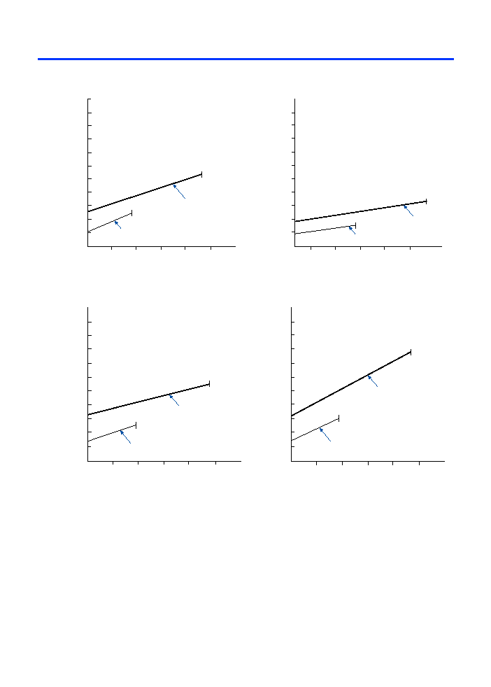
shows typical supply current versus frequency for MAX 9000
devices.
Table 22. MAX 9000 I
CC
Equation Constants
Device
Constant A
Constant B
Constant C
EPM9320
0.81
0.33
0.056
EPM9320A
0.56
0.31
0.024
EPM9400
0.60
0.33
0.053
EPM9480
0.68
0.29
0.064
EPM9560
0.68
0.26
0.052
EPM9560A
0.56
0.31
0.024
34
Altera Corporation
MAX 9000 Programmable Logic Device Family Data Sheet
Figure 15. I
CC
vs. Frequency for MAX 9000 Devices (Part 1 of 2)
0
Frequency (MHz)
1000
200
400
600
800
50
75
100
125
25
EPM9320
118 MHz
Turbo
Frequency (MHz)
0
1000
200
400
600
800
50
75
100
125
25
EPM9320A
144 MHz
Turbo
59 MHz
42 MHz
Non-Turbo
Non-Turbo
Typical
I
CC
Active
(mA)
Typical
I
CC
Active
(mA)
0
Frequency (MHz)
42 MHz
42 MHz
1000
200
400
600
800
50
75
100
125
25
EPM9400
118 MHz
Turbo
0
Frequency (MHz)
1000
200
400
600
800
50
75
100
125
25
EPM9480
118 MHz
Turbo
Non-Turbo
Non-Turbo
Typical
I
CC
Active
(mA)
Typical
I
CC
Active
(mA)
Altera Corporation
35
MAX 9000 Programmable Logic Device Family Data Sheet
Figure 15. I
CC
vs. Frequency for MAX 9000 Devices (Part 2 of 2)
Device
Pin-Outs
Tables 23
through
26
show the dedicated pin names and numbers for each
EPM9320, EPM9320A, EPM9400, EPM9480, EPM9560, and EPM9560A
device package.
0
Frequency (MHz)
42 MHz
59 MHz
1000
200
400
600
800
50
75
100
125
25
EPM9560
118 MHz
Turbo
0
Frequency (MHz)
1000
200
400
600
800
50
75
100
125
25
EPM9560A
144 MHz
Turbo
Non-Turbo
Non-Turbo
Typical
I
CC
Active
(mA)
Typical
I
CC
Active
(mA)
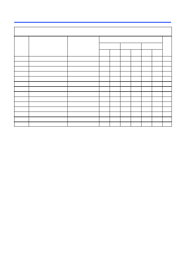
Table 23. EPM9320 & EPM9320A Dedicated Pin-Outs (Part 1 of 2)
Note (1)
Pin Name
84-Pin PLCC
(2)
208-Pin RQFP
280-Pin PGA
(3)
356-Pin BGA
DIN1
(
GCLK1
)
1
182
V10
AD13
DIN2
(
GCLK2
)
84
183
U10
AF14
DIN3
(
GCLR
) 13
153
V17
AD1
DIN4
(
GOE
)
72
4
W2
AC24
TCK
43
78
A9
A18
TMS
55
49
D6
E23
TDI
42
79
C11
A13
TDO
30
108
A18
D3
36
Altera Corporation
MAX 9000 Programmable Logic Device Family Data Sheet
GND
6, 18, 24, 25, 48,
61, 67, 70
14, 20, 24, 31, 35,
41, 42, 43, 44, 46,
47, 66, 85, 102,
110, 113, 114, 115,
116, 118, 121, 122,
132, 133, 143, 152,
170, 189, 206
D4, D5, D16, E4, E5, E6,
E15, E16, F5, F15, G5,
G15, H5, H15, J5, J15, K5,
K15, L5, L15, M5, M15, N5,
N15, P4, P5, P15, P16, R4,
R5, R15, R16, T4, T5, T16
A9, A22, A25, A26, B25,
B26, D2, E1, E26, F2, G1,
G25, G26, H2, J1, J25, J26,
K2, L26, M26, N1, N25,
P26, R2, T1, U2, U26, V1,
V25, W25, Y26, AA2, AB1,
AB26, AC26, AE1, AF1,
AF2, AF4, AF7, AF20
VCCINT
(5.0 V only)
14, 21, 28, 57,
64, 71
10, 19, 30, 45, 112,
128, 139, 148
D15, E8, E10, E12, E14,
R7, R9, R11, R13, R14,
T14
D26, F1, H1, K26, N26, P1,
U1, W26, AE26, AF25,
AF26
VCCIO
(3.3 or 5.0 V)
15, 37, 60, 79
5, 25, 36, 55, 72,
91, 111, 127, 138,
159, 176, 195
D14, E7, E9, E11, E13, R6,
R8, R10, R12, T13, T15
A1, A2, A21, B1, B10, B24,
D1, H26, K1, M25, R1, V26,
AA1, AC25, AF5, AF8,
AF19
No Connect
(N.C.)
29
6, 7, 8, 9, 11, 12,
13, 15, 16, 17, 18,
109, 140, 141, 142,
144, 145, 146, 147,
149, 150, 151
B6, K19, L2, L4, L18, L19,
M1, M2, M3, M4, M16, M17,
M18, M19, N1, N2, N3, N4,
N16, N17, N18, N19, P1,
P2, P3, P17, P18, P19, R1,
R2, R3, R17, R18, R19, T1,
T2, T3, T17, T18, T19, U1,
U2, U3, U17, U18, U19, V1,
V2, V19, W1
B4, B5, B6, B7, B8, B9,
B11, B12, B13, B14, B15,
B16, B18, B19, B20, B21,
B22, B23, C4, C23, D4,
D23, E4, E22, F4, F23, G4,
H4, H23, J23, K4, L4, L23,
N4, P4, P23, R3, R26, T2,
T3, T4, T5, T22, T23, T24,
T25, T26, U3, U4, U5, U22,
U23, U24, U25, V2, V3, V4,
V5, V22, V23, V24, W1,
W2, W3, W4, W5, W22,
W23, W24, Y1, Y2, Y3, Y4,
Y5, Y22, Y23, Y24, Y25,
AA3, AA4, AA5, AA22,
AA23, AA24, AA25, AA26,
AB2, AB3, AB4, AB5,
AB23, AB24, AB25, AC1,
AC2, AC23, AD4, AD23,
AE4, AE5, AE6, AE7, AE9,
AE11, AE12, AE14, AE15,
AE16, AE18, AE19, AE20,
AE21, AE22, AE23
VPP
(4)
56
48
C4
E25
Total User
I/O Pins
(5)
60
132
168
168
Table 23. EPM9320 & EPM9320A Dedicated Pin-Outs (Part 2 of 2)
Note (1)
Pin Name
84-Pin PLCC
(2)
208-Pin RQFP
280-Pin PGA
(3)
356-Pin BGA
Altera Corporation
37
MAX 9000 Programmable Logic Device Family Data Sheet
Notes:
(1)
All pins not listed are user I/O pins.
(2)
Perform a complete thermal analysis before committing a design to this device package. See
Application Note 74
(Evaluating Power for Altera Devices)
.
(3)
EPM9320A devices are not offered in this package.
(4)
During in-system programming, each device's
VPP
pin must be connected to the 5.0-V power supply. During
normal device operation, the
VPP
pin is pulled up internally and can be connected to the 5.0-V supply or left
unconnected.
(5)
The user I/O pin count includes dedicated input pins and all I/O pins.
Notes:
(1)
All pins not listed are user I/O pins.
(2)
Perform a complete thermal analysis before committing a design to this device package. See
Application Note 74
(Evaluating Power for Altera Devices)
for more information.
(3)
During in-system programming, each device's
VPP
pin must be connected to the 5.0-V power supply. During
normal device operation, the
VPP
pin is pulled up internally and can be connected to the 5.0-V supply or left
unconnected.
(4)
The user I/O pin count includes dedicated input pins and all I/O pins.
Table 24. EPM9400 Dedicated Pin-Outs
Note (1)
Pin Name
84-Pin PLCC
(2)
208-Pin RQFP
240-Pin RQFP
DIN1
(
GCLK1
)
2
182
210
DIN2
(
GCLK2
)
1
183
211
DIN3
(
GCLR
)
12
153
187
DIN4
(
GOE
)
74
4
234
TCK
43
78
91
TMS
54
49
68
TDI
42
79
92
TDO
31
108
114
GND
6, 13, 20, 26, 27, 47, 60,
66, 69, 73
14, 20, 24, 31, 35, 41, 42,
43, 44, 46, 47, 66, 85, 102,
110, 113, 114, 115, 116,
118, 121, 122, 132, 133,
143, 152, 170, 189, 206
5, 14, 25, 34, 45, 54, 65,
66, 81, 96, 110, 115, 126,
127, 146, 147, 166, 167,
186, 200, 216, 229
VCCINT
(5.0 V only)
16, 23, 30, 56, 63, 70
10, 19, 30, 45, 112, 128,
139, 148
4, 24, 44, 64, 117, 137,
157, 177
VCCIO
(3.3 or 5.0 V)
17, 37, 59, 80
5, 25, 36, 55, 72, 91, 111,
127, 138, 159, 176, 195
15, 35, 55, 73, 86, 101,
116, 136, 156, 176, 192,
205, 220, 235
No Connect (N.C.)
≠
6, 7, 8, 9, 11, 12, 13, 109,
144, 145, 146, 147, 149,
150, 151
1, 2, 3, 6, 7, 8, 9, 10, 11,
12, 13, 168, 169, 170,
171, 172, 173, 174, 175,
178, 179, 180, 181, 182,
183, 184, 185, 236, 237,
238, 239, 240
VPP
(3)
55
48
67
Total User I/O Pins
(4)
59
139
159

38
Altera Corporation
MAX 9000 Programmable Logic Device Family Data Sheet
Notes:
(1)
All pins not listed are user I/O pins.
(2)
During in-system programming, each device's
VPP
pin must be connected to the
5.0-V power supply. During normal device operation, the
VPP
pin is pulled up
internally and can be connected to the 5.0-V supply or left unconnected.
(3)
The user I/O pin count includes dedicated input pins and all I/O pins.
Table 25. EPM9480 Dedicated Pin-Outs
Note (1)
Pin Name
208-Pin RQFP
240-Pin RQFP
DIN1
(
GCLK1
)
182
210
DIN2
(
GCLK2
)
183
211
DIN3
(
GCLR
)
153
187
DIN4
(
GOE
)
4
234
TCK
78
91
TMS
49
68
TDI
79
92
TDO
108
114
GND
14, 20, 24, 31, 35, 41, 42,
43, 44, 46, 47, 66, 85,
102, 110, 113, 114, 115,
116, 118, 121, 122, 132,
133, 143, 152, 170, 189,
206
5, 14, 25, 34, 45, 54, 65,
66, 81, 96, 110, 115, 126,
127, 146, 147, 166, 167,
186, 200, 216, 229
VCCINT
(5.0 V only)
10, 19, 30, 45, 112, 128,
139, 148
4, 24, 44, 64, 117, 137,
157, 177
VCCIO
(3.3 or 5.0 V)
5, 25, 36, 55, 72, 91, 111,
127, 138, 159, 176, 195
15, 35, 55, 73, 86, 101,
116, 136, 156, 176, 192,
205, 220, 235
No Connect (N.C.)
6, 7, 8, 9, 109, 149, 150,
151
1, 2, 3, 178, 179, 180,
181, 182, 183, 184, 185,
236, 237, 238, 239, 240
VPP
(2)
48
67
Total User I/O Pins
(3)
146
175

Altera Corporation
39
MAX 9000 Programmable Logic Device Family Data Sheet
Table 26. EPM9560 & EPM9560A Dedicated Pin-Outs (Part 1 of 2)
Note (1)
Pin Name
208-Pin RQFP
240-Pin RQFP
280-Pin PGA
(2)
304-Pin RQFP
(2)
356-Pin BGA
DIN1
(
GCLK1
)
182
210
V10
266
AD13
DIN2
(
GCLK2
)
183
211
U10
267
AF14
DIN3
(
GCLR
) 153
187
V17
237
AD1
DIN4
(
GOE
)
4
234
W2
296
AC24
TCK
78
91
A9
114
A18
TMS
49
68
D6
85
E23
TDI
79
92
C11
115
A13
TDO
108
114
A18
144
D3
GND
14, 20, 24, 31, 35,
41, 42, 43, 44, 46,
47, 66, 85, 102,
110, 113, 114,
115, 116, 118,
121, 122, 132,
133, 143, 152,
170, 189, 206
5, 14, 25, 34, 45,
54, 65, 66, 81, 96,
110, 115, 126,
127, 146, 147,
166, 167, 186,
200, 216, 229
D4, D5, D16, E4,
E5, E6, E15, E16,
F5, F15, G5, G15,
H5, H15, J5, J15,
K5, K15, L5, L15,
M5, M15, N5,
N15, P4, P5, P15,
P16, R4, R5, R15,
R16, T4, T5, T16
13, 22, 33, 42, 53,
62, 73, 74, 102,
121, 138, 155,
166, 167, 186,
187, 206, 207,
226, 254, 273,
290
A9, A22, A25,
A26, B25, B26,
D2, E1, E26, F2,
G1, G25, G26,
H2, J1, J25, J26,
K2, L26, M26, N1,
N25, P26, R2, T1,
U2, U26, V1, V25,
W25, Y26, AA2,
AB1, AB26,
AC26, AE1, AF1,
AF2, AF4, AF7,
AF20
VCCINT
(5.0 V only)
10, 19, 30, 45,
112, 128, 139,
148
4, 24, 44, 64, 117,
137, 157, 177
D15, E8, E10,
E12, E14, R7, R9,
R11, R13, R14,
T14
12, 32, 52, 72,
157, 177, 197,
217
D26, F1, H1, K26,
N26, P1, U1,
W26, AE26,
AF25, AF26
VCCIO
(3.3 or 5.0 V)
5, 25, 36, 55, 72,
91, 111, 127, 138,
159, 176, 195
15, 35, 55, 73, 86,
101, 116, 136,
156, 176, 192,
205, 220, 235
D14, E7, E9, E11,
E13, R6, R8, R10,
R12, T13, T15
3, 23, 43, 63, 91,
108, 127, 156,
176, 196, 216,
243, 260, 279
A1, A2, A21, B1,
B10, B24, D1,
H26, K1, M25,
R1, V26, AA1,
AC25, AF5, AF8,
AF19
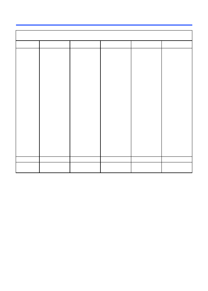
40
Altera Corporation
MAX 9000 Programmable Logic Device Family Data Sheet
Notes:
(1)
All pins not listed are user I/O pins.
(2)
EPM9560A devices are not offered in this package.
(3)
During in-system programming, each device's
VPP
pin must be connected to the 5.0-V power supply. During
normal device operation, the
VPP
pin is pulled up internally and can be connected to the 5.0-V supply or left
unconnected.
(4)
The user I/O pin count includes dedicated input pins and all I/O pins.
No Connect
(N.C.)
109
≠
B6, W1
1, 2, 76, 77, 78,
79, 80, 81, 82, 83,
84, 145, 146, 147,
148, 149, 150,
151, 152, 153,
154, 227, 228,
229, 230, 231,
232, 233, 234,
235, 236, 297,
298, 299, 300,
301, 302, 303,
304
B4, B5, B6, B7,
B8, B9, B11, B12,
B13, B14, B15,
B16, B18, B19,
B20, B21, B22,
B23, C4, C23, D4,
D23, E4, E22, F4,
F23, G4, H4, H23,
J23, K4, L4, L23,
N4, P4, P23, T4,
T23, U4, V4, V23,
W4, Y4, AA4,
AA23, AB4,
AB23, AC23,
AD4, AD23, AE4,
AE5, AE6, AE7,
AE9, AE11,
AE12, AE14,
AE15, AE16,
AE18, AE19,
AE20, AE21,
AE22, AE23
VPP
(3)
48
67
C4
75
E25
Total User
I/O Pins
(4)
153
191
216
216
216
Table 26. EPM9560 & EPM9560A Dedicated Pin-Outs (Part 2 of 2)
Note (1)
Pin Name
208-Pin RQFP
240-Pin RQFP
280-Pin PGA
(2)
304-Pin RQFP
(2)
356-Pin BGA

Altera Corporation
41
MAX 9000 Programmable Logic Device Family Data Sheet
Revision
History
Information contained in the MAX 9000 Programmable Logic Device Family
Data Sheet version 6.4 supersedes information published in previous
versions.
Version 6.4
Version 6.4 of the MAX 9000 Programmable Logic Device Family Data Sheet
contains the following change:Updated text on
page 19
.
Version 6.3
Version 6.3 of the MAX 9000 Programmable Logic Device Family Data Sheet
contains the following change: added
Note
(7)
to
Table 13
.

Copyright © 2002 Altera Corporation. All rights reserved. Altera, The Programmable Solutions Company, the
stylized Altera logo, specific device designations, and all other words and logos that are identified as
trademarks and/or service marks are, unless noted otherwise, the trademarks and service marks of Altera
Corporation in the U.S. and other countries. All other product or service names are the property of their
respective holders. Altera products are protected under numerous U.S. and foreign patents and pending
applications, maskwork rights, and copyrights. Altera warrants performance of its semiconductor products to
current specifications in accordance with Altera's standard warranty, but reserves the right to make changes
to any products and services at any time without notice. Altera assumes no responsibility
or liability arising out of the application or use of any information, product, or service
described herein except as expressly agreed to in writing by Altera Corporation. Altera
customers are advised to obtain the latest version of device specifications before relying on
any published information and before placing orders for products or services.
101 Innovation Drive
San Jose, CA 95134
(408) 544-7000
http://www.altera.com
Applications Hotline:
(800) 800-EPLD
Customer Marketing:
(408) 544-7104
Literature Services:
lit_req@altera.com
Æ
MAX 9000 Programmable Logic Device Family Data Sheet
42
Altera Corporation
Printed on Recycled Paper.