Document Outline
- FLEX 6000 Programmable Logic Device Family
Æ
Altera Corporation
1
FLEX 6000
Programmable Logic
Device Family
March 2001, ver. 4.1
Data Sheet
A-DS-F6000-04.1
Features...
s
Provides an ideal low-cost, programmable alternative to high-
volume gate array applications and allows fast design changes
during prototyping or design testing
s
Product features
≠
Register-rich, look-up table- (LUT-) based architecture
≠
OptiFLEX
Æ
architecture that increases device area efficiency
≠
Typical gates ranging from 5,000 to 24,000 gates (see
Table 1
)
≠
Built-in low-skew clock distribution tree
≠
100% functional testing of all devices; test vectors or scan chains
are not required
s
System-level features
≠
In-circuit reconfigurability (ICR) via external configuration
device or intelligent controller
≠
5.0-V devices are fully compliant with peripheral component
interconnect Special Interest Group (PCI SIG) PCI Local Bus
Specification, Revision 2.2
≠
Built-in Joint Test Action Group (JTAG) boundary-scan test
(BST) circuitry compliant with IEEE Std. 1149.1-1990, available
without consuming additional device logic
≠
MultiVolt
TM
I/O interface operation, allowing a device to bridge
between systems operating at different voltages
≠
Low power consumption (typical specification less than 0.5 mA
in standby mode)
≠
3.3-V devices support hot-socketing
Note:
(1)
The embedded IEEE Std. 1149.1 JTAG circuitry adds up to 14,000 gates in addition to the listed typical gates.
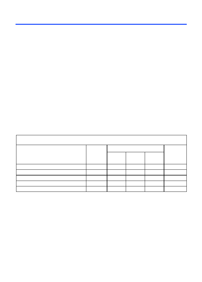
Table 1. FLEX 6000 Device Features
Feature
EPF6010A
EPF6016
EPF6016A
EPF6024A
Typical gates
(1)
10,000
16,000
16,000
24,000
Logic elements (LEs)
880
1,320
1,320
1,960
Maximum I/O pins
102
204
171
218
Supply voltage (V
CCINT
)
3.3 V
5.0 V
3.3 V
3.3 V

2
Altera Corporation
FLEX 6000 Programmable Logic Device Family Data Sheet
...and More
Features
s
Powerful I/O pins
≠
Individual tri-state output enable control for each pin
≠
Programmable output slew-rate control to reduce switching
noise
≠
Fast path from register to I/O pin for fast clock-to-output time
s
Flexible interconnect
≠
FastTrack
Æ
Interconnect continuous routing structure for fast,
predictable interconnect delays
≠
Dedicated carry chain that implements arithmetic functions such
as fast adders, counters, and comparators (automatically used by
software tools and megafunctions)
≠
Dedicated cascade chain that implements high-speed, high-fan-
in logic functions (automatically used by software tools and
megafunctions)
≠
Tri-state emulation that implements internal tri-state networks
≠
Four low-skew global paths for clock, clear, preset, or logic
signals
s
Software design support and automatic place-and-route provided by
Altera's development system for Windows-based PCs, Sun
SPARCstations, and HP 9000 Series 700/800
s
Flexible package options
≠
Available in a variety of packages with 100 to 256 pins, including
the innovative FineLine BGA
TM
packages (see
Table 2
)
≠
SameFrame
TM
pin-compatibility (with other FLEX
Æ
6000 devices)
across device densities and pin counts
≠
Thin quad flat pack (TQFP), plastic quad flat pack (PQFP), and
ball-grid array (BGA) packages (see
Table 2
)
≠
Footprint- and pin-compatibility with other FLEX 6000 devices
in the same package
s
Additional design entry and simulation support provided by
EDIF 2 0 0 and 3 0 0 netlist files, the library of parameterized modules
(LPM), Verilog HDL, VHDL, DesignWare components, and other
interfaces to popular EDA tools from manufacturers such as
Cadence, Exemplar Logic, Mentor Graphics, OrCAD, Synopsys,
Synplicity, VeriBest, and Viewlogic
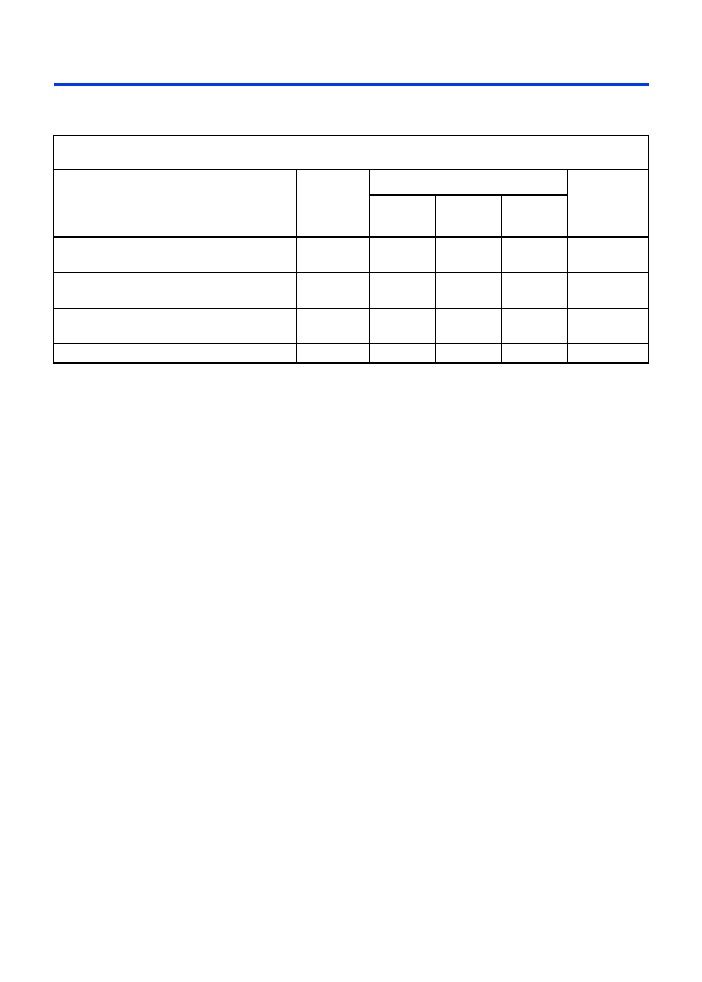
Table 2. FLEX 6000 Package Options & I/O Pin Count
Device
100-Pin
TQFP
100-Pin
FineLine BGA
144-Pin
TQFP
208-Pin
PQFP
240-Pin
PQFP
256-Pin
BGA
256-pin
FineLine BGA
EPF6010A
71
102
EPF6016
117
171
199
204
EPF6016A
81
81
117
171
171
EPF6024A
117
171
199
218
219
Altera Corporation
3
FLEX 6000 Programmable Logic Device Family Data Sheet
General
Description
The Altera
Æ
FLEX 6000 programmable logic device (PLD) family provides
a low-cost alternative to high-volume gate array designs. FLEX 6000
devices are based on the OptiFLEX architecture, which minimizes die size
while maintaining high performance and routability. The devices have
reconfigurable SRAM elements, which give designers the flexibility to
quickly change their designs during prototyping and design testing.
Designers can also change functionality during operation via in-circuit
reconfiguration.
FLEX 6000 devices are reprogrammable, and they are 100
%
tested prior to
shipment. As a result, designers are not required to generate test vectors
for fault coverage purposes, allowing them to focus on simulation and
design verification. In addition, the designer does not need to manage
inventories of different gate array designs. FLEX 6000 devices are
configured on the board for the specific functionality required.
Table 3
shows FLEX 6000 performance for some common designs. All
performance values shown were obtained using Synopsys DesignWare or
LPM functions. Special design techniques are not required to implement
the applications; the designer simply infers or instantiates a function in a
Verilog HDL, VHDL, Altera Hardware Description Language (AHDL), or
schematic design file.
Note:
(1)
This performance value is measured as a pin-to-pin delay.
Table 3. FLEX 6000 Device Performance for Common Designs
Application
LEs Used
Performance
Units
-1 Speed
Grade
-2 Speed
Grade
-3 Speed
Grade
16-bit loadable counter
16
172
153
133
MHz
16-bit accumulator
16
172
153
133
MHz
24-bit accumulator
24
136
123
108
MHz
16-to-1 multiplexer (pin-to-pin)
(1)
10
12.1
13.4
16.6
ns
16
◊
16 multiplier with a 4-stage pipeline
592
84
67
58
MHz
4
Altera Corporation
FLEX 6000 Programmable Logic Device Family Data Sheet
Table 4
shows FLEX 6000 performance for more complex designs.
Note:
(1)
The applications in this table were created using Altera MegaCore
TM
functions
.
FLEX 6000 devices are supported by Altera development systems; a
single, integrated package that offers schematic, text (including AHDL),
and waveform design entry, compilation and logic synthesis, full
simulation and worst-case timing analysis, and device configuration. The
Altera software provides EDIF 2 0 0 and 3 0 0, LPM, VHDL, Verilog HDL,
and other interfaces for additional design entry and simulation support
from other industry-standard PC- and UNIX workstation-based EDA
tools.
The Altera software works easily with common gate array EDA tools for
synthesis and simulation. For example, the Altera software can generate
Verilog HDL files for simulation with tools such as Cadence Verilog-XL.
Additionally, the Altera software contains EDA libraries that use device-
specific features such as carry chains which are used for fast counter and
arithmetic functions. For instance, the Synopsys Design Compiler library
supplied with the Altera development systems include DesignWare
functions that are optimized for the FLEX 6000 architecture.
The Altera development system runs on Windows-based PCs, Sun
SPARCstations, and HP 9000 Series 700/800.
f
See the
MAX+PLUS II Programmable Logic Development System & Software
Data Sheet
and the
Quartus Programmable Logic Development System &
Software Data Sheet
for more information.
Table 4. FLEX 6000 Device Performance for Complex Designs
Note (1)
Application
LEs Used
Performance
Units
-1 Speed
Grade
-2 Speed
Grade
-3 Speed
Grade
8-bit, 16-tap parallel finite impulse response
(FIR) filter
599
94
80
72
MSPS
8-bit, 512-point fast Fourier transform (FFT)
function
1,182
75
63
89
53
109
43
µ
S
MHz
a16450
universal asynchronous
receiver/transmitter (UART)
487
36
30
25
MHz
PCI bus target with zero wait states
609
56
49
42
MHz

Altera Corporation
5
FLEX 6000 Programmable Logic Device Family Data Sheet
Functional
Description
The FLEX 6000 OptiFLEX architecture consists of logic elements (LEs).
Each LE includes a 4-input look-up table (LUT), which can implement any
4-input function, a register, and dedicated paths for carry and cascade
chain functions. Because each LE contains a register, a design can be easily
pipelined without consuming more LEs. The specified gate count for
FLEX 6000 devices includes all LUTs and registers.
LEs are combined into groups called logic array blocks (LABs); each LAB
contains 10 LEs. The Altera software automatically places related LEs into
the same LAB, minimizing the number of required interconnects. Each
LAB can implement a medium-sized block of logic, such as a counter or
multiplexer.
Signal interconnections within FLEX 6000 devices--and to and from
device pins--are provided via the routing structure of the FastTrack
Interconnect. The routing structure is a series of fast, continuous row and
column channels that run the entire length and width of the device. Any
LE or pin can feed or be fed by any other LE or pin via the FastTrack
Interconnect. See "FastTrack Interconnect" on
page 17
of this data sheet
for more information.
Each I/O pin is fed by an I/O element (IOE) located at the end of each row
and column of the FastTrack Interconnect. Each IOE contains a
bidirectional I/O buffer. Each IOE is placed next to an LAB, where it can
be driven by the local interconnect of that LAB. This feature allows fast
clock-to-output times of less than 8 ns when a pin is driven by any of the
10 LEs in the adjacent LAB. Also, any LE can drive any pin via the row and
column interconnect. I/O pins can drive the LE registers via the row and
column interconnect, providing setup times as low as 2 ns and hold times
of 0 ns. IOEs provide a variety of features, such as JTAG BST support,
slew-rate control, and tri-state buffers.
Figure 1
shows a block diagram of the FLEX 6000 OptiFLEX architecture.
Each group of ten LEs is combined into an LAB, and the LABs are
arranged into rows and columns. The LABs are interconnected by the
FastTrack Interconnect. IOEs are located at the end of each FastTrack
Interconnect row and column.