Document Outline
- QFP Carrier Development Socket Data Sheet

Æ
Altera Corporation
1
QFP Carrier &
Development Socket
August 1999, ver. 13
Data Sheet
A-DS-QFP-13
General
13
Information
Features
s
Quad flat pack (QFP) carriers protect fragile leads on QFP devices
during shipping and device handling.
s
QFP development sockets allow on-board electrical and mechanical
prototype testing with QFP packages.
s
Carriers and development sockets are available for 100-, 160-, 208-,
240-, and 304-pin devices.
s
Development socket footprints are compatible with QFP footprints,
providing a smooth transition from prototype to production.
s
Together, carriers and sockets help prevent electrostatic damage to
the devices while providing excellent AC circuit performance.
General
Description
Altera QFP carriers and development sockets protect the fragile leads on
QFP devices during shipping and throughout the development cycle.
Each socket is designed with a lead footprint that is compatible with the
device, so it can be used during both mechanical and electrical
prototyping. QFP carriers and development sockets are currently
available for 100-, 160-, 208-, 240-, and 304-pin QFP packages.
Figure 1
shows the carrier and development socket for the 100-pin QFP device (the
160- and 208-pin QFP carriers and development sockets are similar).
Figure 1. 100-Pin QFP Carrier & Development Socket
Development
Socket Base
Development
Socket Lid
QFP Carrier
QFP Device
Beveled Corner
Indicates Location
of Pin 1

2
Altera Corporation
QFP Carrier & Development Socket Data Sheet
Figure 2
shows the carrier and development socket for the 240-pin QFP
device (the 304-pin QFP carrier and development socket are similar).
Figure 2. 240-Pin QFP Carrier & Development Socket
QFP Carrier
The carrier is a static-dissipative, molded plastic shell that holds the QFP
device in a secure frame to prevent mechanical damage to the device
leads. The device is held in the carrier by recessed plastic clips (two clips
on the 100-pin carrier and four clips on the 160-, 208-, 240-, and 304-pin
carriers).
Figure 3
shows the dimensions of the QFP carriers.
All MAX 9000, MAX 7000, MAX 3000 and MAX 5000 QFP devices with
100 to 304 pins can be ordered in carriers, which eliminates the need to
handle the delicate device leads. The devices and carriers are packaged in
antistatic rails.
Devices can be programmed and erased while in the carrier. EPROM-
based QFP devices are erased with a UV lamp; EEPROM-based QFP
devices are erased electrically in a programming adapter.
1
QFP devices without protective carriers should be handled with
a vacuum wand in an electrostatically protected workplace to
reduce the possibility of mechanical or electrical device damage.
Development
Socket Lid
Development
Socket Base
QFP Carrier &
QFP Device
Lid Removal
Tool
Beveled Corner
Indicates Location
of Pin 1
Press

Altera Corporation
3
QFP Carrier & Development Socket Data Sheet
General
13
Information
Figure 3. QFP Carrier Dimensions
Dimensions are shown in millimeters. The carrier is rated from ≠65∞ C to 155∞ C, and is qualified to handle commercial and
industrial operating temperatures. Illustrations are not drawn to scale.
Pin Count
L
W
H
100
25.2
21.2
4.2
160
33.2
35.2
5.1
208
33.2
35.2
5.1
240
37.0
40.0
6.4
304
45.0
48.0
6.4
Indicates
Location
of Pin 1
L
W
H
100-Pin QFP Carrier
L
W
160- & 208-Pin QFP Carrier
Indicates
Location
of Pin 1
Indicates
Pin Count
160
H
L
W
240- & 304-Pin QFP Carrier
Indicates
Location
of Pin 1
Indicates
Pin Count
240
Pin 1
H

4
Altera Corporation
QFP Carrier & Development Socket Data Sheet
QFP
Development
Socket
The QFP development socket footprint is compatible with the lead
footprint of the QFP device. The socket ensures the device's electrical
connection to the printed circuit board (PCB) and provides excellent AC
circuit performance, including low noise, low capacitance, and low
inductance. Although the QFP development socket is designed to
minimize noise, interconnect capacitance, and inductance, these effects
can be further reduced by mounting the device directly on the PCB for
production.
1
Altera recommends using the QFP development socket for
prototyping only. Altera does not recommend using sockets for
production.
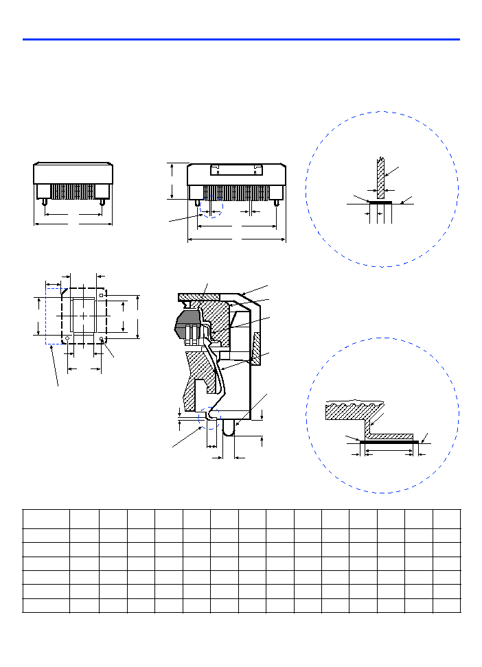
Figure 4
shows the dimensions of the QFP development socket. Details A
and B show the PCB pad layout length and width recommended for use
with the development socket. These industry-standard pad layout
dimensions are for the "gull-wing" lead that is typically found on QFP
packages. The layout pad extends from 0.05 mm to 0.13 mm beyond each
side of the lead width (A1), and 0.5 mm beyond each side of the lead
length (A2), as shown in Details A and B, respectively. A layout pad of
these dimensions is also suitable for use with QFP devices that do not use
carriers. To ensure correct board layout, pad sizes must be compatible
with the development socket and the QFP device leads.
Altera Corporation
5
QFP Carrier & Development Socket Data Sheet
General
13
Information
Figure 4. QFP Development Socket Dimensions
Dimensions are shown in millimeters. The tolerance of all layout pad dimensions is ±0.025 mm. The continuous duty rating
for the development socket is ≠65∞ C to 155∞ C. The carrier and development socket are qualified to handle commercial
and industrial operating temperatures.
Pin Count
A1
A2
A3
B1
B2
C
D1
D2
E1
E2
F1
F2
P1
P2
100
0.20
0.93
0.65
25.00 19.00 12.00 31.51 25.54 23.63 17.63 18.85 12.35
1.00
1.50
160
0.20
0.93
0.65
33.80 33.80 12.80 39.80 39.80 32.08 32.08 25.35 25.35
1.00
1.50
208
0.20
0.93
0.50
33.82 33.82 12.80 39.80 39.80 31.68 31.68 25.50 25.50
1.00
1.50
240
0.20
0.93
0.50
34.00 34.00 14.30 44.00 42.90 35.20 35.20 29.50 29.50
1.00
1.50
304
0.20
0.93
0.50
42.00 42.00 14.30 52.00 50.90 43.30 43.30 37.50 37.50
1.00
1.50
Tolerance
±
0.12
±
0.12
±
0.12
±
0.12
±
0.12
±
0.40
±
0.20
±
0.20
±
0.12
±
0.12
±
0.12
±
0.12
±
0.12
±
0.12
B1
F1
E1
F2
Development Socket
Package
Lead
QFP Carrier
Alignment
Post
Contact
A2
C
A1
B1
Recommended Board Layout
Contact & Lid Detail
D1
D2
E2
QFP Device
P1
P2
.25
A3
BSC
Development Socket Width
Development Socket Length
B2
B2
Diameter = 1.19
See Detail B
See Detail A
Detail B
A2
Contact
Development
Socket Base
Layout Pad
(Length)
0.5
0.5
Detail A
A1
Development
Socket Lead
0.05 ≠ 0.13
Layout
Pad
Board
For 240- and 304-pin QFP
packages, leave this space
for removal of development
socket lid.
4.5
Board