 | –≠–ª–µ–∫—Ç—Ä–æ–Ω–Ω—ã–π –∫–æ–º–ø–æ–Ω–µ–Ω—Ç: ES3044 | –°–∫–∞—á–∞—Ç—å:  PDF PDF  ZIP ZIP |
1
EV3083/S3044
SONET/SDH OC-48 TRANSCEIVER EVALUATION BOARD
August 5, 1999
EV3083/S3044
Æ
SONET/SDH OC-48 TRANSCEIVER EVALUATION BOARD
DESCRIPTION
The S3083/S3044 Evaluation Board provides a flexible platform for verifying the operation of the S3083/S3044
transceiver interface circuit. This document provides information on the board contents. It should be used in
conjunction with the S3083 and S3044 data sheets, which contains the full technical details on the chips
operation.
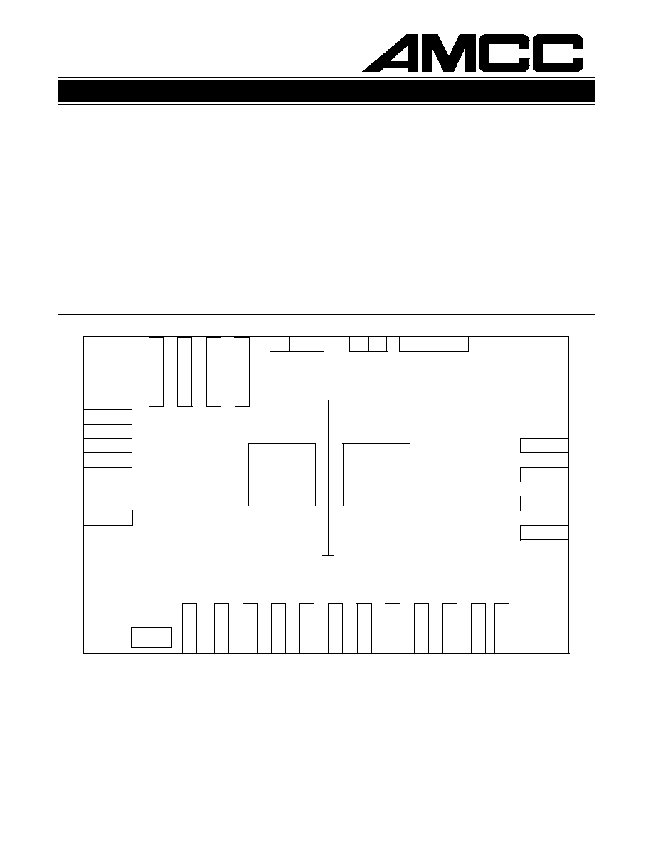
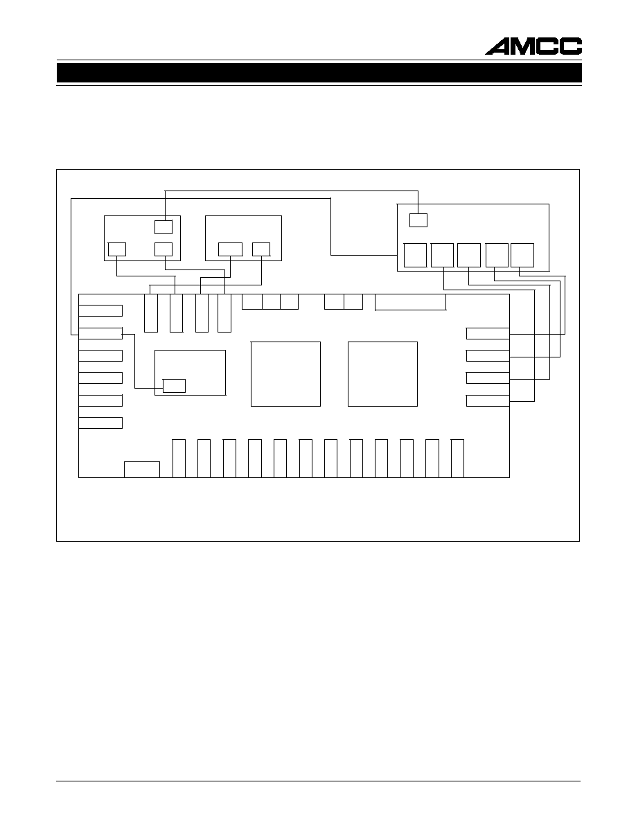
Figure 1 shows the outline of the S3083/S3044 Evaluation Board, and Figure 5 shows the block diagram of how
the S3083/S3044 Evaluation Board should be connected to test equipment for Bit Error Rate (BER) testing. In
this configuration the S3083/S3044 is configured for use with the internal VCO, using a 155.52 MHz reference
and operating at STS-48/STM-16 rate. Figure 6 shows the block diagram for jitter generation testing of the
S3083/S3044 Evaluation Board with jitter analyzer test equipment. Figure 7 shows the block diagram for Line
Loopback (LLEB) mode. Figure 8 shows the block diagram for Diagnostic Loopback (DLEB) mode.
Figure 1. Evaluation Board Top View
REFCLKN
REFCLKP
LSCLKP
LSCLKN
LSDP
LSDN
RSCLKN
RSCLKP
RSDN
RSDP
DS1
TSCLKP
TSCLKN
TSDP
TSDN
LLCLKP
LLCLKN
LLDP
LLDN
LLDN
LLDP
LLCLKN
LLCLKP
LSDN
LSDP
LSCLKN
LSCLKP
S3083 TX
S3044 RX
VEE
-3.3V GND
VEE
-3.3V
GND
DS1
-5.2V
RSTB
1. Note: DS = Dip Switch
2
EV3083/S3044
SONET/SDH OC-48 TRANSCEIVER EVALUATION BOARD
August 5, 1999
S3083
TX
VCC
EXTERNAL
REFCLK
155MHz or
2.4GHz
PCLKP
LSDP
LSCLKP
NC
155MCK
LOCKDET
PHERR
LSCLKN
TSCLKN
TSDP
TSDN
TSCLKP
REFCLKN
REFCLKP
10K
1K
TESTEN
RSTB
DLEB
LLEB
AVCC
LLDP
LLCLKP
PICLKP
CAP1
LLCLKN
LLDN
1K
RSTB
PICLKN
PCLKN
LSDN
GND
CAP1
75
75
2.2uF
-3.3V
10K
PHINIT
45
43
20
22
21
23
24
47
54
55
56
57
77
78
13
9
8
5
11
12
14
15
67
66
VCC - 3, 16, 17, 41, 48, 50, 52, 59, 60,
62, 64, 70
AVCC - 69, 72, 74, 80
HEL33
DIVIDE
BY 4
HEL33
DIVIDE
BY 4
-5.2V
-5.2V
330
0.1uF/100pF
0.1uF/100pF
0.001uF
330
51
1
2
6
7
10K
VEE - 4, 10, 18, 19, 42, 51, 53, 58, 61,
63, 65, 75,
AVEE - 68, 71, 73, 79
10uF
VEE = -3.3V
GND
10uF
-5.2V
0
0
-5.2V
-5.2V
0805 "0"
Ohm jumper:
P0.0GCT-ND
Inductor = 0603, 600 Ohms at 100 MHz Ferrite
Bead: BLM11A601SPTM00-03
L
VEE
VCC
AVCC
25
26
27
28
29
30
31
32
33
34
35
36
37
38
39
40
PIN15
PIN0
PIN1
PIN2
PIN3
PIN4
PIN5
PIN6
PIN7
PIN8
PIN9
PIN10
PIN11
PIN12
PIN13
PIN14
46
1
2
A
B
*
* With a 155MHz clock, position 1 is used and switch A and B are closed.
With a 2.4GHz clock, position 2 is used and switch A and B are open
330
330
330
VEE
PINxx
100 to 400
TX Input Termination
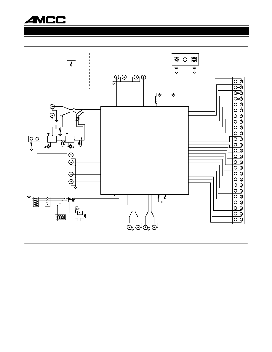
Figure 2. Schematic of the S3083 Evaluation Board
3
EV3083/S3044
SONET/SDH OC-48 TRANSCEIVER EVALUATION BOARD
August 5, 1999
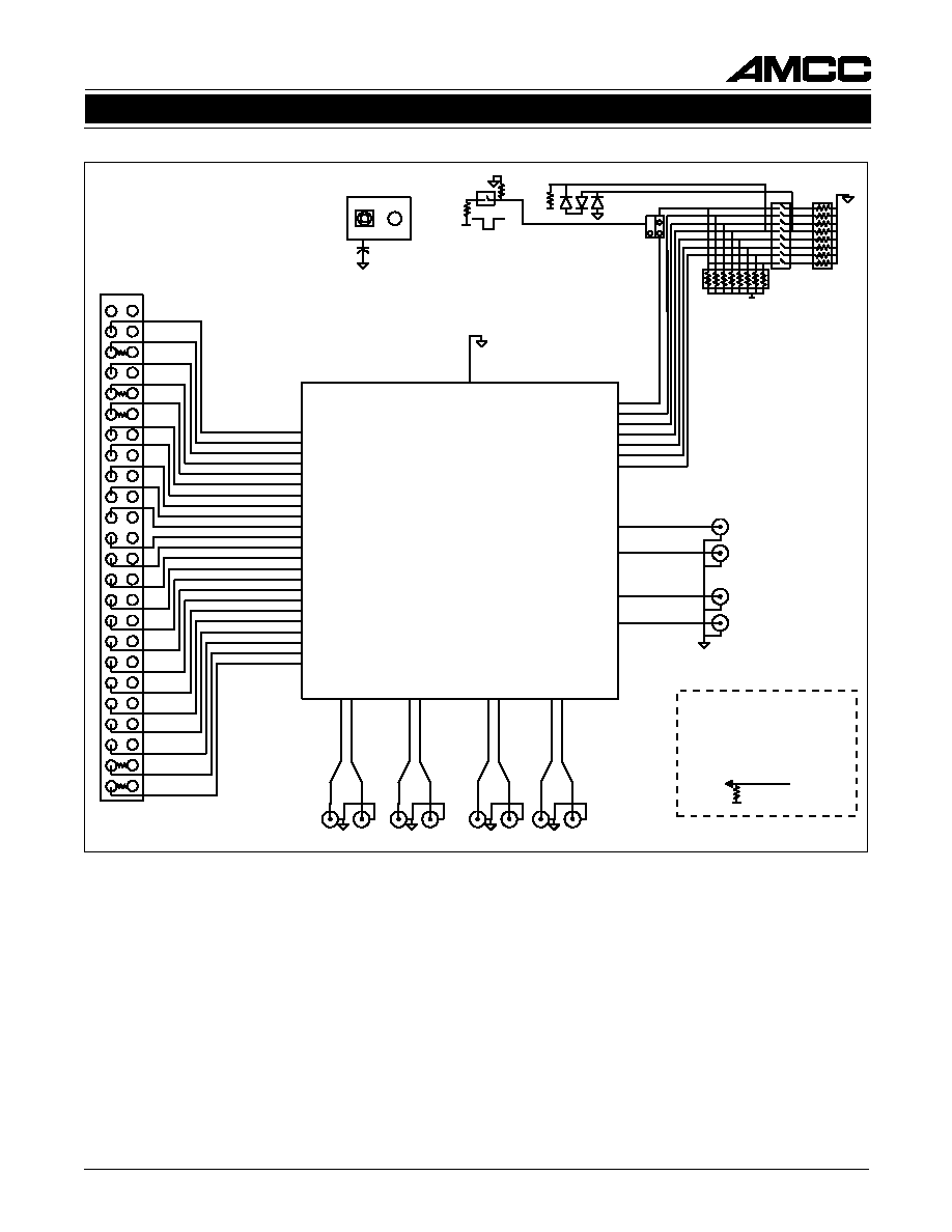
Figure 3. Schematic of the S3044 Evaluation Board
VCC
GND
31
30
25
29
51
52
28
S3044
RX
10K
1K
-3.3V
1K
RSTB
10K
NC
OOF
FRAMEN
KILLRXCLK
SDPECL
LLEB
DLEB
RSTB
SEARCH
FP
OVREF
POCLKP
RX155MCKP
10uF
VEE = -3.3V GND
1K
VEE
RX155MCKN
THD
POUT0
POUT1
POUT2
POUT3
POUT4
POUT5
POUT6
POUT7
POUT8
POUT9
POUT10
POUT11
POUT12
POUT13
POUT14
POUT15
POCLKN
16
17
18
19
22
23
24
VCC - 1, 5, 9, 11, 13, 15, 26, 42, 54, 56,
64, 67, 72, 76, 78,
POUTxx
100 to 400
RX OUTPUT
TERMINATION
VEE - 2, 6, 10, 12, 14, 21, 27, 40,
41, 53, 55, 63, 66, 71, 75, 77
LSDN
LSDP
LSCLKN
LSCLKP
LLCLKP
LLCKKN
LLDP
LLDN
61
62
68
69
73
74
79
80
VEE
RSCLKN
RSDN
RSCLKP
RSDP
3
4
7
8
VCC
50
32
33
34
35
36
37
38
39
43
44
45
46
47
48
49
Diodes:
IN 4002
9711
330
330
330
330
330

4
EV3083/S3044
SONET/SDH OC-48 TRANSCEIVER EVALUATION BOARD
August 5, 1999
6, 14, 21, 27,
53, 55, 63, 66, 71,
75, 77
2
40, 41
S3044 RX Power and Ground
Connections
0603 X7R Capacitors
Ground (VCC) = 1, 5, 9, 11, 13, 15, 26, 42,
54, 56, 64, 67, 72, 76, 78
100pF
0.1
µ
F
VEE
100pF
0.1
µ
F
1
µ
F
VEE
100pF
0.1
µ
F
100pF
0.1
µ
F
VEE
Pins 10, 12 are tied to VEE
S3083 TX Power and Ground
Connections
4, 10, 18, 19, 42,
51, 53, 58, 75, 79
61, 63, 65
VCO_GND 68
VCO_POW 69
71, 73
72, 74, 80
Ground (VCC) = 3, 16, 17, 41, 48, 50,
52, 59, 60, 62, 64, 70
100pF
0.1
µ
F
VEE
100pF
0.1
µ
F
0.1
µ
F
100pF
VEE
L
L
0.1
µ
F
100pF
VEE
L
L
Inductors (L) = 0603, 600 Ohms at 100
MHz Ferrite Bead: BLM11A601SPTM00-03
Capacitors 0603 X7R
Figure 4. Power and Ground Connections
5
EV3083/S3044
SONET/SDH OC-48 TRANSCEIVER EVALUATION BOARD
August 5, 1999
Figure 5 depicts how the S3083/S3044 Evaluation board can be connected for BER measurements, and shows
all of the dip switch settings and the power supply requirements for use with test equipment that utilizes 50 ohms
to ground termination.
Figure 5. BER Test Setup (S3083/S3044 Setup for Normal Operation Serial In Serial Out)
REFCLKN
REFCLKP
LSCLKP
LSCLKN
LSDP
LSDN
RSCLKN
RSCLKP
RSDN
RSDP
DS1
VEE
-3.3V
GND -5.2V
S3083 TX
VEE
-3.3V
GND
S3044 RX
DS2
TSCLKP
TSCLKN
TSDP
TSDN
LLCLKP
LLCLKN
LLDP
LLDN
LLDN
LLDP
LLCLKN
LLCLKP
LSDN
LSDP
LSCLKN
LSCLKP
DIVIDE BY 16
INPUT
ANRITSU MP1650A PULSE GENERATOR
DSO TEK CSA
803A
ANRITSU MP1653A
ERROR DETECTOR
CH1
CH2
TRIG
IN
DATA
IN
CLK
IN
CLK
DATA
CLK
OUT1
/CLK
OUT1
CLK/
16
SWITCH SETTING:
DS1:
LLEB=1
DLEB=1
RSTB=1
TESTN= 0
DS2:
RSTB=1
DLEB=1
LLEB=1
SDPECL=1
KILLRXCLK=1
FRAME=0
OOF=1
NC=1
/DATA
OUT
DATA
OUT
Pattern