 | –≠–ª–µ–∫—Ç—Ä–æ–Ω–Ω—ã–π –∫–æ–º–ø–æ–Ω–µ–Ω—Ç: EV2002 | –°–∫–∞—á–∞—Ç—å:  PDF PDF  ZIP ZIP |
Part Number EV2002
Revision 1.0 - April 13, 2000
EV2002
Dual Serial Backplane Device
1
EVALUATION BOARD
Introduction
The S2002 evaluation board provides a flexible platform for verifying the operation of the S2002 Dual Serial Back-
plane Device. This document provides information on the S2002 evaluation board's contents and layout. It should
be used in conjunction with the S2002 product data sheet. Contact your local AMCC field applications engineer or
regional sales manager to discuss any questions or concerns you may have.
EV2002 Kit Contents
S2002 evaluation board
EV2002 device specification (This document)
Two minicoax cables labeled as "Cable #1" (To loop back clock in parallel loopback configuration)
Two minicoax cables labeled as "Cable #2" (To loop back KFLAGx, KGENx, and DNx in parallel loopback
configuration)
Board Description
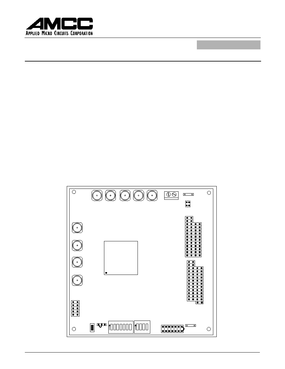
The top view of the S2002 evaluation board is shown in Figure 1. The high-speed differential LVPECL receive
RXxP/N, and transmit TXxP/N signals (where lower case "x" is A and B for each channel) are brought in and out of
the device on SMA connectors, as shown on the top and left edges of the board. The reference clock is brought in
through the SMA connector labeled as REFCLK.
Figure 1. S2002 Evaluation Board
*ERRB in the S2002 data sheet is labeled as "ERRC" on the S2002 evaluation board.
AMCC
Applied Micro Circuits Corp.
6290 Sequence Dr.
San Diego, CA 92121
S2002 Evaluation Board
AMCC
S2002
GND
GND
GND
GND
I/P
O/P
DNB
KGENB
DINB7
DINB6
DINB5
DINB4
DINB3
DINB2
DINB1
DINB0
TCLKB
RCBP
RCBN
ERRC
KFLAGB
DOUTB7
DOUTB6
DOUTB5
DOUTB4
DOUTB3
DOUTB2
DOUTB1
DOUTB0
EOFB
DNA
KGENA
DINA7
DINA6
DINA5
DINA4
DINA3
DINA2
DINA1
DINA0
TCLKA
TCLK0
RCAP
RCAN
ERRA
KFLAGA
DOUTA7
DOUTA6
DOUTA5
DOUTA4
DOUTA3
DOUTA2
DOUTA1
DOUTA0
EOFA
REFCLK
TXAN
TXAP
RXAP
RXAN
RXBP
RXBN
RESET
TXBN
TXBP
VDD GND
"1"
"0"
1 2 3 4 5 6 7
ON
GND
REFCLK(S)
DINB7(S)
1 2 3 4
ON
TDO
TCK
TMS
TDI
TRS
FR SW
TO DUT
FR DIPSWITCH
RESET
LPENA
LPENB
MODE
TMODE
RATE
CLKSEL
SYNC
LC BYP
CMODE
TESTMODE
DOUTB3
DINB2
TCLKB
DINB3
DIND0
DIND2
TESTMODE1
*
1
A
2
EV2002 ≠Dual Serial Backplane Device
EVALUATION BOARD
Revision 1.0 - April 13, 2000
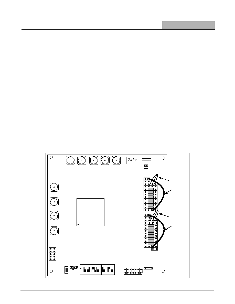
Parallel Loopback Test Setup
Typical tests performed with the S2002 evaluation board are Bit Error Rate Testing (BERT) and jitter testing. In each
case, it is easiest to configure the evaluation board for serial input and output (I/O), looping back the parallel I/O with
jumpers. The serial I/O (parallel loopback) configuration is shown in Figure 2 and is described below.
DIP switch settings for parallel loopback, where low = logic 0 and high = logic 1, are:
Signal Name
DIP Switch Setting
LPENA
low
LPENB
low
TMODE
high
RATE
high or low (determined by the desired serial data rate)
CLKSEL
high or low (determined by the desired reference clock rate)
SYNC
low
CMODE
high
TESTMODE
low
In order to configure the board for parallel loopback, the parallel input data must be clocked into the device with the
TCLKx input clocks as shown in Figure 2. This clock is provided by looping the RCxP output clock back into the
respective TCLKx input with one of the minicoax cables labeled as "Cable #1" that are provided in the EV2002 kit.
Also, in this test configuration, the KFLAGx output must be looped back into the DNx and KGENx inputs by using
the minicoax cables labeled as "Cable #2" that are provided in the EV2002 kit. These cables need only be con-
nected for the channel(s) under test.
Figure 2. Parallel Loopback Configuration
AMCC
S2002 Evaluation Board
AMCC
S2002
GND
GND
GND
GND
I/P
O/P
DNB
KGENB
DINB7
DINB6
DINB5
DINB4
DINB3
DINB2
DINB1
DINB0
TCLKB
RCBP
RCBN
ERRC
KFLAGB
DOUTB7
DOUTB6
DOUTB5
DOUTB4
DOUTB3
DOUTB2
DOUTB1
DOUTB0
EOFB
DNA
KGENA
DINA7
DINA6
DINA5
DINA4
DINA3
DINA2
DINA1
DINA0
TCLKA
TCLK0
RCAP
RCAN
ERRA
KFLAGA
DOUTA7
DOUTA6
DOUTA5
DOUTA4
DOUTA3
DOUTA2
DOUTA1
DOUTA0
EOFA
REFCLK
TXAN
TXAP
RXAP
RXAN
RXBP
RXBN
RESET
TXBN
TXBP
VDD GND
"1"
"0"
1 2 3 4 5 6 7
ON
GND
REFCLK(S)
DINB7(S)
1 2 3 4
ON
TDO
TCK
TMS
TDI
TRS
FR SW
TO DUT
FR DIPSWITCH
RESET
LPENA
LPENB
MODE
TMODE
RATE
CLKSEL
SYNC
LC BYP
CMODE
TESTMODE
DOUTB3
DINB2
TCLKB
DINB3
DIND0
DIND2
TESTMODE1
1
A
Cable #1
Cable #1
Cable #2
Cable #2

3
EV2002 ≠ Dual Serial Backplane Device
EVALUATION BOARD
Revision 1.0 - April 13, 2000
Electrical Connections
Power Connections
A terminal post is provided on the top edge of the board for the power and ground connections to the S2002 Dual
Serial Backplane Device. The S2002 voltage is specified at +3.3 V +/-5%.
Parallel I/O Header Terminals
Parallel input and output (I/O) signals are brought in and out on the connector banks on the right edge of the board.
There is one connector bank for each channel (A and B).
DINx[0:7] ≠ Data In. TTL input. Transmit Data for Channels A and B. Parallel data on this bus is clocked in on the
rising edge of TCLKx or REFCLK.
KGENx ≠ K-Character Generation. TTL input. KGENA high causes the data on DINA[0:7] to be encoded into a K-
Character. (See S2002 data sheet).
DNx ≠ Data_Not. TTL input. When low, data present on DINx[0:7] is 8B/10B encoded and transmitted serially.
When high, special character/sequences are generated as indicated in the S2002 data sheet.
DOUTx[0:7] ≠ Data Out. TTL output. Receive Data Outputs for Channels A and B. Parallel data on this bus is valid
on the rising edge of RCxP in full clock mode, and valid on the rising edge of both RCxP and RCxN in half clock
mode.
KFLAGx ≠ K-Character Flag. TTL output. A high on KFLAGx indicates that a valid control character has been
detected.
ERRx ≠ Receive Error. TTL output. A high on ERRx indicates the occurrence of either a parity error or an invalid
codeword error during decoding of the received data.
TCLKx ≠ Transmit Clock. TTL input. When TMODE is high, this signal is used to clock data on DINx[0:7], DNx, and
KGENx into the S2002. When TMODE is low, TCLKx is ignored.
TCLKO ≠ Transmit Clock Out. TTL output. TTL Output Clock at the parallel data rate. This clock is provided for use
by upstream circuitry.
RCxP/N ≠ Receive Clock. TTL output. Parallel receive data, DOUTx[0:7], KFLAGx, ERRx, and EOFx are valid on
the rising edge of RCxP when in full clock mode, and valid on the rising edge of both RCxP and RCxN in half clock
mode.
EOFx ≠ End of Frame Detect. TTL output. A high on EOFx indicates that a valid K28.5 has been detected and is
present on the parallel data outputs DOUTx[0:7].
TDO ≠ Test Data Out. TTL output (tristate). JTAG data output. Can be high impedance under JTAG controller
command.
TCK ≠ Test Clock. TTL input. JTAG test clock.
TMS ≠ Test Mode Select. TTL input. Enables JTAG testing of device.
TDI ≠ Test Data In. TTL input. JTAG data input.
TRS ≠ Test Reset. TTL input. Resets JTAG test state machine.
FR SW ≠ Provided with a jumper to TO DUT to enable the push-button RESET on the evaluation board.
TO DUT ≠ Provided with a jumper to FR SW to enable the push-button RESET on the evaluation board.
FR DIPSWITCH ≠ Not used for this device.
REFCLK(S), DNB7(S) ≠ Not used for this device.
DOUTB3, DINB2, TCLKB, DINB3, DIND0, DIND2 ≠ Not used for this device.
TESTMODE1 ≠ Test Mode Control. Provided with a jumper to logic 0 for normal operation.
4
EV2002 ≠Dual Serial Backplane Device
EVALUATION BOARD
Revision 1.0 - April 13, 2000
SMA Connectors
RXxP/N ≠ Receive Serial Data for Channels A or B. Differential LVPECL inputs.
TXxP/N ≠ Transmit Serial Data for Channels A or B. Differential LVPECL outputs.
REFCLK ≠ Reference Clock. TTL input. Clock used for the transmit VCO and frequency check for the clock recov-
ered from the receiver serial data.
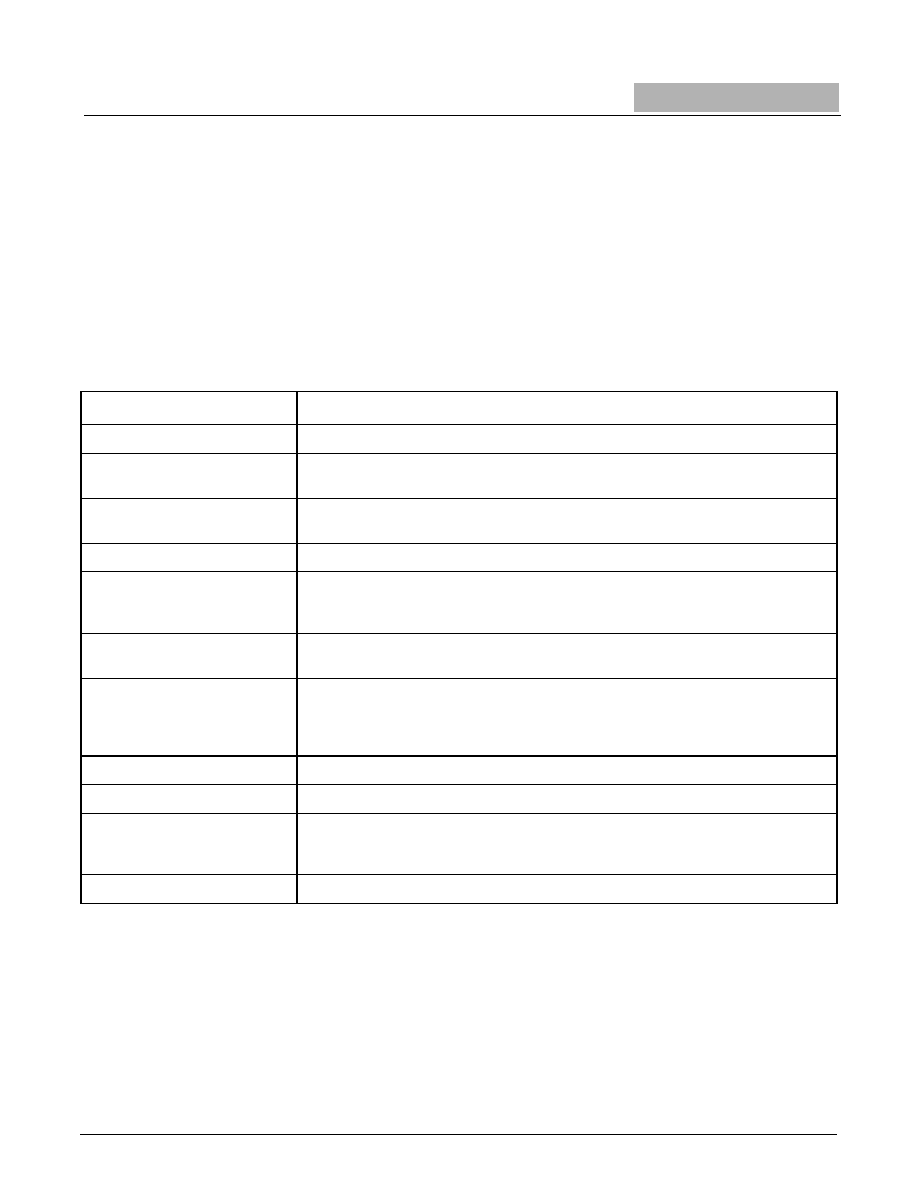
DIP Switches
The S2002 evaluation board is provided with DIP switches at the bottom of the board to control the static functions
of the on-board device. DIP switch settings are outlined in Table 1. Moving the switch to the "ON" position creates
a logic 1 (high), moving it away from the "ON" setting creates a logic 0 (low).
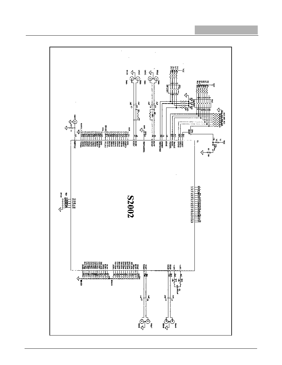
Schematic and Bill of Materials
The S2002 evaluation board schematic is shown in Figure 3. The power and ground connections for the S2002 eval-
uation board are shown in Figure 4. The bill of materials for the S2002 evaluation board is provided in Tables 2 and 3.
Table 1. DIP Switch Settings
DIP Name
Description
RESET
Not used for this device. Use push-button RESET instead.
LPENA
Loopback Enable Channel A. When low, the device performs normal transceiver opera-
tion. When high the serial output for each channel is looped back to its input.
LPENB
Loopback Enable Channel B. When low, the device performs normal transceiver opera-
tion. When high the serial output for each channel is looped back to its input.
MODE
Not used for this device.
TMODE
Transfer Mode Control. When TMODE is low, REFCLK is used to clock data on
DINx[0:7], DNx, SYNC, and KGENx into the S2002. When TMODE is high, TCLKx is
used to clock data into the S2002.
RATE
When low the S2002 operates with the serial output rate equal to the VCO frequency.
When high the S2002 operates with the VCO internally divided by 2 for all functions.
CLKSEL
REFCLK Select input. This signal configures the PLL for the appropriate REFCLK fre-
quency. When CLKSEL = 0, the REFCLK frequency equals the parallel data rate. When
CLKSEL = 1, the REFCLK frequency is half the parallel data rate (and is internally x2
multiplied).
SYNC
When high, used to generate a special sequence of K28.5 characters.
LC BYP
Not used for this device.
CMODE
Clock Mode Control. When low, the rate of the parallel output clock (RCxP/N) is half the
data rate. When high, the rate of the parallel output clock (RCxP/N) is equal to the data
rate.
TESTMODE
Test Mode Control. Low for normal operation.
5
EV2002 ≠ Dual Serial Backplane Device
EVALUATION BOARD
Revision 1.0 - April 13, 2000
Figure 3. S2002 Evaluation Board Schematic