 | –≠–ª–µ–∫—Ç—Ä–æ–Ω–Ω—ã–π –∫–æ–º–ø–æ–Ω–µ–Ω—Ç: EV2060QF | –°–∫–∞—á–∞—Ç—å:  PDF PDF  ZIP ZIP |
1
EV2060
GIGABIT ETHERNET TRANSCEIVER EVALUATION BOARDS
REVISION 4.0
May 9, 2000
EV2060
Æ
GIGABIT ETHERNET TRANSCEIVER EVALUATION BOARDS
REVISION 4.0
EVALUATION BOARD OVERVIEW
This document describes operation and usage of the S2060 evaluation boards. The evaluation boards allow
users to become familiar with the functionality of the S2060 Gigabit Ethernet Transceiver. Specifically, Bit Error
Rate (BER), jitter, and basic performance can be tested using the evaluation boards. This document provides a
complete board description, explains various test configurations, and contains a bill of materials with a corre-
sponding schematic. This document should be used in conjunction with the S2060 data sheet and application
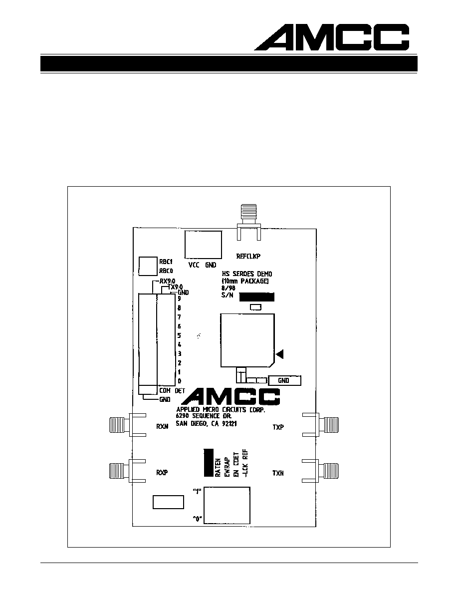
note. Figure 1 shows an outline of the S2060A evaluation board.
Figure 1. S2060 Evaluation Board
GND
A
A
A
B
C
D
D
D
A
A
2
EV2060
GIGABIT ETHERNET TRANSCEIVER EVALUATION BOARDS
REVISION 4.0
May 9, 2000
EVALUATION BOARD DESCRIPTION
This section describes the functionality of the connectors and settings recommended for the S2060 evaluation
boards. Brief descriptions of the SMA connectors on board, dip switch descriptions and settings, power and
grounds, output levels, header settings, and probes are presented. The letters "A", "B", "C", and "D" correspond
to specific parts on the evaluation board shown in Figure 1, and are described in the following section according
to their letter designation in Figure 1.
[A] SMA Connectors
SMA connectors are provided for the differential serial data input/output signals and output clock. Additional
SMA connectors are provided for an optional differential serial input clock, the external TTL reference clock and
the optional external parallel input clock. Table 1 gives a description of the SMA connectors.
Table 1. SMA Connectors
s
r
o
t
c
e
n
n
o
C
n
o
i
t
p
i
r
c
s
e
D
)
N
X
R
/
P
X
R
(
a
t
a
D
l
a
i
r
e
S
e
v
i
e
c
e
R
0
6
0
2
S
e
h
t
f
o
s
t
u
p
n
i
a
t
a
d
l
a
i
r
e
S
.
s
t
u
p
n
i
l
a
i
t
n
e
r
e
f
f
i
D
)
N
X
T
/
P
X
T
(
t
u
p
t
u
O
a
t
a
D
l
a
i
r
e
S
t
i
m
s
n
a
r
T
.
a
t
a
d
t
u
p
t
u
o
a
t
a
d
l
a
i
r
e
S
.
s
t
u
p
t
u
o
l
a
i
t
n
e
r
e
f
f
i
D
)
K
L
C
F
E
R
(
k
c
o
l
C
e
c
n
e
r
e
f
e
R
.
g
n
i
k
c
o
l
c
e
c
n
e
r
e
f
e
R
e
m
a
N
p
i
D
n
o
i
t
p
i
r
c
s
e
D
N
E
T
A
R
e
h
t
r
o
f
s
'
L
L
P
e
h
t
s
e
r
u
g
i
f
n
o
c
l
a
n
g
i
s
s
i
h
T
.
w
o
L
e
v
i
t
c
A
.
t
c
e
l
e
S
e
t
a
R
5
2
6
s
i
e
g
n
a
r
g
n
i
t
a
r
e
p
o
e
h
t
,
e
v
i
t
c
a
n
i
n
e
h
W
.
y
c
n
e
u
q
e
r
f
C
B
T
e
t
a
i
r
p
o
r
p
p
a
.
z
H
G
5
2
.
1
s
i
e
g
n
a
r
g
n
i
t
a
r
e
p
o
e
h
t
,
e
v
i
t
c
a
n
e
h
W
.
z
H
M
P
A
R
W
E
s
t
u
p
t
u
o
a
t
a
d
l
a
i
r
e
s
r
e
t
t
i
m
s
n
a
r
t
e
h
t
,
e
v
i
t
c
a
n
e
h
W
.
h
g
i
H
e
v
i
t
c
A
.
p
a
r
W
e
l
b
a
n
E
c
i
t
a
t
s
e
r
a
N
/
P
X
T
.
s
t
u
p
n
i
a
t
a
d
l
a
i
r
e
s
r
e
v
i
e
c
e
r
e
h
t
o
t
d
e
t
u
o
r
y
ll
a
n
r
e
t
n
i
e
r
a
d
e
t
c
e
l
e
s
e
r
a
s
t
u
p
n
i
l
a
i
r
e
s
N
/
P
X
R
e
h
t
,
e
v
i
t
c
a
n
i
n
e
h
W
.
e
t
a
t
s
s
i
h
t
n
i
)
1
c
i
g
o
l
(
.
)
n
o
i
t
a
r
e
p
o
l
a
m
r
o
n
(
T
E
D
C
_
N
E
e
h
t
f
o
n
o
i
t
c
e
t
e
d
s
e
l
b
a
n
e
,
e
v
i
t
c
a
n
e
h
W
.
h
g
i
H
e
v
i
t
c
A
.
t
c
e
t
e
D
a
m
m
o
C
e
l
b
a
n
E
.
w
o
ll
o
f
o
t
a
t
a
d
e
h
t
r
o
f
y
r
a
d
n
u
o
b
e
m
a
r
f
d
r
o
w
e
h
t
t
e
s
o
t
n
r
e
t
t
a
p
c
n
y
s
a
m
m
o
c
.
d
e
m
a
r
f
n
u
s
a
d
e
t
a
e
r
t
s
i
a
t
a
d
,
e
v
i
t
c
a
n
i
n
e
h
W
F
E
R
_
K
C
L
-
e
v
i
e
c
e
r
e
h
t
,
n
e
p
o
r
o
e
v
i
t
c
a
n
i
n
e
h
W
.
w
o
L
e
v
i
t
c
A
.
t
u
p
n
I
e
c
n
e
r
e
f
e
R
o
t
k
c
o
L
e
h
t
,
e
v
i
t
c
a
n
e
h
W
.
)
n
o
i
t
a
r
e
p
o
l
a
m
r
o
n
(
a
t
a
d
g
n
i
m
o
c
n
i
e
h
t
o
t
k
c
o
l
ll
i
w
L
L
P
.
t
u
p
n
i
C
B
T
e
h
t
o
t
k
c
o
l
o
t
d
e
c
r
o
f
s
i
L
L
P
e
v
i
e
c
e
r
Table 2. Dip Switch Functional Description
[B] Dip Switches
The evaluation board is equipped with a DIP switch to control the static control functions of the on-board
devices. For both arrays the OFF (open = "0") condition of the DIP switch asserts a logic low on the assigned
signal, and the ON (closed = "1") condition asserts a logic high. Note that "0" and "1" are printed on the
evaluation board. Table 2 shows the functional DIP switch descriptions. Table 3 shows DIP switch settings
corresponding to the tests described at the end of this document.
3
EV2060
GIGABIT ETHERNET TRANSCEIVER EVALUATION BOARDS
REVISION 4.0
May 9, 2000
t
o
N
(
)
d
e
l
e
b
a
L
N
E
T
A
R
P
A
R
W
E
T
E
D
C
_
N
E
F
E
R
_
K
C
L
-
T
S
E
T
R
E
B
0
1
0
0
1
T
S
E
T
R
E
T
T
I
J
0
1
0
0
1
Table 3. Dip Switch Settings for Test and Evaluation Configurations
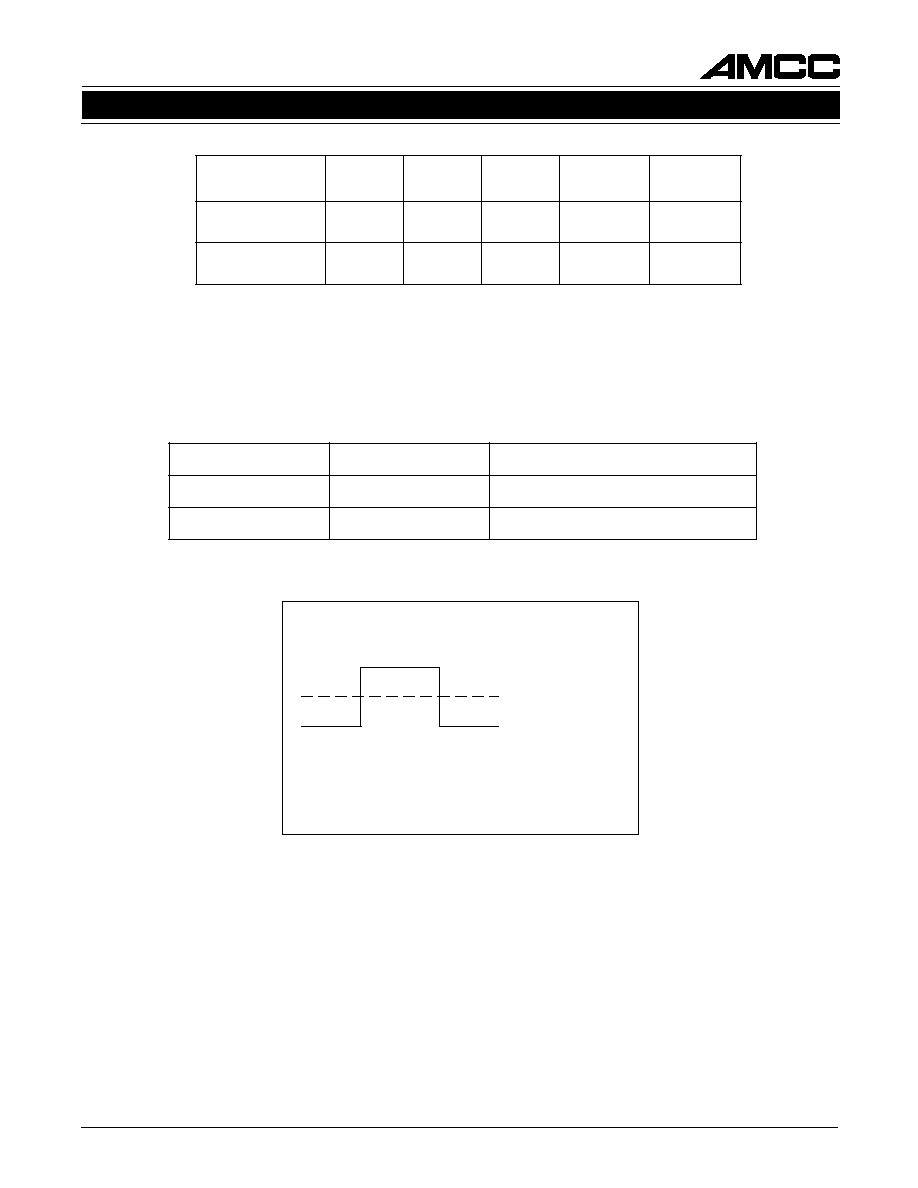
Table 4. S2060 Power and Ground Values
VOH
VOL
Termination = 50
to (VCC-2V)
or 150
to VEE
Vcc -1.3 V (internal
DC bias point)
Figure 2. Single-Ended LVPECL Output Swing
[C] Power/Ground
Three terminal outputs are provided at the top edge of the board for Vcc and Vee. The S2060 is specified for 3.3
V +/- 5%.
The TXP/N single-ended LVPECL output swing is shown in Figure 2. The bias point is internally set 1.3 volts
below the Vcc rail. As discussed in both the S2060 data sheet and application note, 150
pulldown resistors are
recommended on the positive and negative outputs for full output voltage swing. Test equipment inputs, how-
ever, typically provide 50
loads. When interfacing to test equipment the Vcc and Vee input levels may be
shifted to 2.0 V and ≠1.3 V respectively in order to maintain full voltage swing with the smaller load. Table 4
summarizes the voltage rail settings and associated output loading.
t
s
o
P
l
a
n
i
m
r
e
T
c
c
V
t
s
o
P
l
a
n
i
m
r
e
T
e
e
V
n
o
i
t
a
n
i
m
r
e
T
t
u
p
t
u
O
L
C
E
P
V
L
V
3
.
3
V
0
.
2
0
5
1
e
e
V
o
t
V
0
.
2
V
3
.
1
≠
0
5
c
c
V
o
t
)
D
N
G
(
V
0
.
2
≠

4
EV2060
GIGABIT ETHERNET TRANSCEIVER EVALUATION BOARDS
REVISION 4.0
May 9, 2000
Table 5. Evaluation Board Header Descriptions
r
e
d
a
e
H
n
o
i
t
p
i
r
c
s
e
D
1
C
B
R
0
C
B
R
s
i
a
t
a
d
e
v
i
e
c
e
r
l
e
ll
a
r
a
p
,
e
d
o
m
e
t
a
r
ll
u
f
n
I
.
s
k
c
o
l
C
e
t
y
B
e
v
i
e
c
e
R
y
r
a
t
n
e
m
e
l
p
m
o
C
d
il
a
v
s
i
a
t
a
d
t
u
p
t
u
o
,
e
t
a
r
f
l
a
h
r
o
F
.
1
C
B
R
d
n
a
0
C
B
R
f
o
s
e
g
d
e
g
n
i
s
i
r
e
h
t
n
o
d
il
a
v
.
1
C
B
R
f
o
e
g
d
e
g
n
i
s
i
r
e
h
t
n
o
T
E
D
_
M
O
C
s
e
t
a
c
i
d
n
i
T
E
D
_
M
O
C
,
e
v
i
t
c
a
s
i
T
E
D
C
_
N
E
n
e
h
W
.
h
g
i
H
e
v
i
t
c
A
.
t
c
e
t
e
D
a
m
m
o
C
n
o
p
U
.
]
9
:
0
[
X
R
s
t
i
b
s
u
b
l
e
ll
a
r
a
p
e
h
t
n
o
t
n
e
s
e
r
p
s
i
r
e
t
c
a
r
a
h
c
c
n
y
s
e
h
t
t
a
h
t
s
i
h
t
)
y
t
i
r
a
l
o
p
e
v
i
t
i
s
o
p
,
x
x
x
1
1
1
1
1
0
0
(
r
e
t
c
a
r
a
h
c
c
n
y
s
a
m
m
o
c
e
h
t
f
o
n
o
i
t
c
e
t
e
d
e
n
o
r
o
f
h
g
i
h
s
n
i
a
m
e
r
d
n
a
1
C
B
R
f
o
e
g
d
e
g
n
i
s
i
r
e
h
t
n
o
d
il
a
v
s
i
a
t
a
d
t
u
p
t
u
o
c
i
g
o
l
(
w
o
l
d
l
e
h
s
i
T
E
D
_
M
O
C
,
e
v
i
t
c
a
n
i
s
i
T
E
D
C
_
N
E
n
e
h
W
.
d
o
i
r
e
p
k
c
o
l
c
1
C
B
R
t
u
p
t
u
o
T
E
D
_
M
O
C
e
h
t
,
t
u
p
n
i
T
E
D
C
_
N
E
e
h
t
f
o
e
t
a
t
s
f
o
e
g
n
a
h
c
n
o
p
U
.
)
0
.
s
e
m
i
t
e
t
y
b
3
f
o
m
u
m
i
x
a
m
a
y
b
d
e
y
a
l
e
d
e
b
ll
i
w
e
s
n
o
p
s
e
r
]
9
:
0
[
X
R
n
o
d
il
a
v
s
i
s
u
b
s
i
h
t
n
o
a
t
a
d
l
e
ll
a
r
a
p
,
t
u
p
t
u
o
e
t
a
r
ll
u
f
r
o
F
.
s
t
u
p
t
u
O
a
t
a
D
e
v
i
e
c
e
R
.
d
e
v
i
e
c
e
r
t
i
b
t
s
r
i
f
e
h
t
s
i
]
0
[
X
R
.
1
C
B
R
d
n
a
0
C
B
R
f
o
s
e
g
d
e
g
n
i
s
i
r
e
h
t
]
9
:
0
[
X
T
.
C
B
T
f
o
e
g
d
e
g
n
i
s
i
r
e
h
t
n
n
i
d
e
k
c
o
l
c
s
i
s
u
b
s
i
h
t
n
o
a
t
a
d
l
e
ll
a
r
a
P
.
a
t
a
D
t
i
m
s
n
a
r
T
.
t
s
r
i
f
d
e
t
t
i
m
s
n
a
r
t
s
i
]
0
[
X
T
D
N
G
.
d
n
u
o
r
G
[D] Probes (Headers)
RCB1, RCB0, and COM_DET are probe points. The output levels of RCB1, RCB0, and COM_DET pins can be
probed during testing. These pins must be left unjumpered.
RX[0:9], TX[0:9] and GND can be either jumpered, utilized as probe points, or utilized as active I/O. RX[0:9] and
TX[0:9] can be jumpered such that parallel output (RX[0:9] ) is bridged directly to the parallel input (TX[0:9]).
Selected RX[0:9] and TX[0:9] pins can also be jumpered to ground to set up a static input configuration. The
probe descriptions are given in Table 5. DUT input and output signals are typically routed to and from the
evaluation board through the serial I/O. Providing evaluation board I/O through the parallel connectors would
require the user to construct a cable harness.
5
EV2060
GIGABIT ETHERNET TRANSCEIVER EVALUATION BOARDS
REVISION 4.0
May 9, 2000
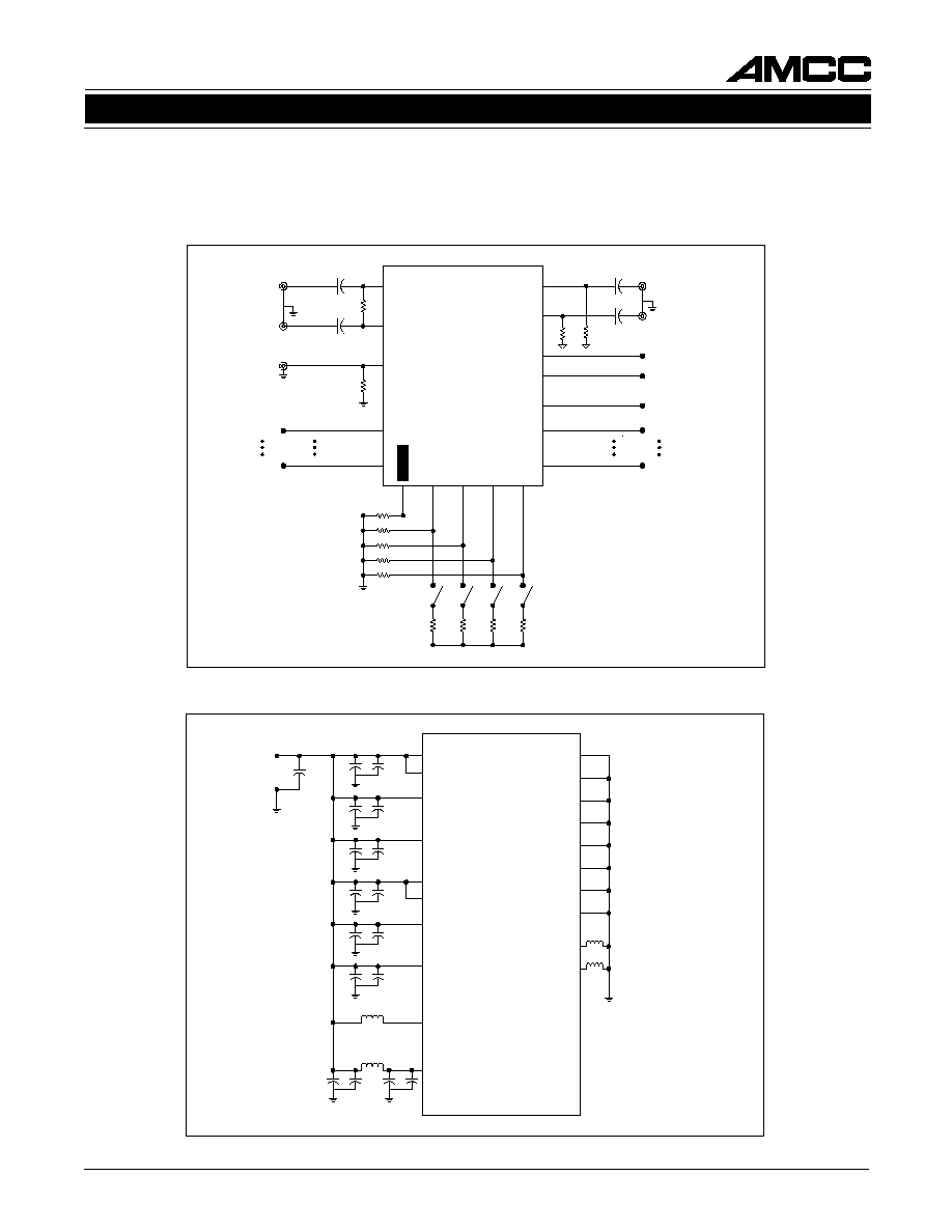
SCHEMATIC/BILL OF MATERIALS
Figures 3 and 4 provide a schematic representation of the evaluation boards. Table 6 lists the Bill of Materials for
the evaluation boards.
Figure 3. Signal Connections
Figure 4. Power and Ground Connections
S2060
C1
R2
R1
R4
R2
R3
R3
RX9
RX0
REFCLKP
RXN
RXP
SMA
SMA
TXP
TXN
RBC0
RBC1
COM-DET
TX0
TX9
RATEN
EWRAP
EN_CDET
LCK_REF
C1
C1
C1
21
25
32
47
56
58
64
15
51
5
21
10
20
23
37
42
55
60
18
50
L
L
L
L
Power
Terminal
(1x2)
Vcc
S2060
C3
C1
C2
C1
C2
C1
C2
C1
C2
C1
C2
C1
C2
C1
C2
C1
C2