 | –≠–ª–µ–∫—Ç—Ä–æ–Ω–Ω—ã–π –∫–æ–º–ø–æ–Ω–µ–Ω—Ç: EV2065 | –°–∫–∞—á–∞—Ç—å:  PDF PDF  ZIP ZIP |
Part Number EV2065
Revision 1.0 - November 18, 1999
EV2065
Quad Serial Backplane Device with Dual I/O
AMCC Confidential and Proprietary
1
EVALUATION BOARD
Introduction
The S2065 evaluation board provides a flexible platform for verifying the operation of the S2065 Quad Serial Back-
plane Device with Dual I/O. This document provides information on the evaluation board's contents. It should be
used in conjunction with the S2065 product data sheet. Contact your local AMCC field applications engineer or
regional sales manager to discuss any questions or concerns you may have.
EV2065 Kit Contents
S2065 evaluation board
EV2065 Device Specification (This document)
Four minicoax cables (To loop back clock in parallel loopback configuration)
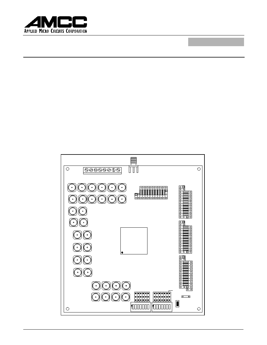
Board Description
The top view of the EV2065 evaluation board is shown in Figure 1. The high speed differential LVPECL receive
RXxP/N, and transmit TXxP/N, where x = A through D, are brought in and out on the SMA connectors, as shown
on the left side of the board.
Figure 1. S2065 Evaluation Board
REFCLK
AMCC
S2065
GND
RCCP
RCCN
ERRC
KFLAGC
DOUTC7
DOUTC6
DOUTC5
DOUTC4
DOUTC3
DOUTC2
DOUTC1
DOUTC0
EOFC
SOFC
KGENC
DINC7
DINC6
DINC5
DINC4
DINC3
DINC2
DINC1
DINC0
TCLKC
SOFB
KGENB
DINB7
DINB6
DINB5
DINB4
DINB3
DINB2
DINB1
DINB0
TCLKB
RCBP
RCBN
ERRB
KFLAGB
DOUTB7
DOUTB6
DOUTB5
DOUTB4
DOUTB3
DOUTB2
DOUTB1
DOUTB0
EOFB
SOFA
KGENA
DINA7
DINA6
DINA5
DINA4
DINA3
DINA2
DINA1
DINA0
TCLKA
TCLK0
RCAP
RCAN
ERRA
KFLAGA
DOUTA7
DOUTA6
DOUTA5
DOUTA4
DOUTA3
DOUTA2
DOUTA1
DOUTA0
EOFA
GND
GND
INPUT
OUTPUT
RCDP
RCDN
ERRD
KFLAGD
DOUTD7
DOUTD6
DOUTD5
DOUTD4
DOUTD3
DOUTD2
DOUTD1
DOUTD0
EOFD
SOFD
KGEND
DIND7
DIND6
DIND5
DIND4
DIND3
DIND2
DIND1
DIND0
TCLKD
GND
GND
O/P
I/P
GND
RX
VDDA
TX
VDD
RX
VDD
PECL
VDD
DIG
VDD
GND
TTL
VDD
AMCC
S2065 Evaluation Board
RX2CP
RX1CN
RX1DP
RX2DP
TX1AN
TX1AP
TX1BP
TX1BN
TX2AN
TX2AP
TX1CN
TX1CP
RESET
TX1DN
TX2BP
TX2CN
TX2DP
TX1DP
TX2BN
TX2CP
TX2DN
RX2DN
RX1DN
RX1CP
RX2CN
RESET
LPEN
RATE
MODE-10
TMODE
CLKSEL
RXSELD
RXSELC
RXSELB
RXSELA
LC BYP
CMODE
CH_LOCK
1 2 3 4 5 6 7
ON
1 2 3 4 5 6 7
ON
GND
RX2BP
RX1BP
RX1AN
RX2AN
RX2BN
RX1BN
RX1AP
RX2AP
1
A
2
AMCC Confidential and Proprietary
EV2065 ≠ Quad Serial Backplane Device
with Dual I/O
EVALUATION BOARD
Revision 1.0 - November 18, 1999
The reference clock is brought in through the SMA connector labeled REFCLK. Power and ground are brought in
through the connector at the top of the board. The S2065 voltage is specified at 3.3V +/- 5%. Parallel Inputs/Out-
puts are brought in and out on the connector banks on the right side of the board; there is one connector bank for
each channel (A through D). Input and output static control signals are controlled with the use of the DIP switches
at the bottom of the board. DIP switch settings are outlined in Tables 1 and 2. Moving the switch to the on position
creates a logic 1 (High), moving it away from the on setting creates a logic 0 (Low). In addition to the DIP switches,
the control signals are brought out on headers. The jumpers must be installed (between middle and bottom pins)
for the DIP switches to be utilized. The top header row is ground, as labeled. Several component sites on the board
are intentionally not populated, including the lower left corner (labled Hewlett Packard). These are designed into
the board for use in factory testing, and are not required for demonstration purposes.
Table 1. DIP Switch 1 Settings
DIP Name
Description
RESET
When Low, the S2065 is held in reset. When High, the S2065 operates normally.
LPEN
Loopback Enable. When Low, the device performs normal transceiver operation. When
High, the serial output for each channel is looped back to its input. The serial outputs are
squelched when LPEN = High.
RATE
When Low, the S2065 operates with the serial output rate equal to the VCO frequency.
When High, the S2065 operates with the VCO internally divided by 2 for all functions.
MODE-10
Test signal. Not connected.
TMODE
Transmit Mode Control. When TMODE is Low, REFCLK is used to clock data on
DINx[7:0], SOFx, and KGENx into the S2065. When TMODE is High, TCLKx is used to
clock data into the S2065. In Channel Lock mode (CH_LOCK HIGH), all four channels
are clocked by TCLKA. In independent mode (CH_LOCK LOW) each channel is clocked
by its respective TCLK.
CLKSEL
REFCLK Select input. This signal configures the PLL for the appropriate REFCLK fre-
quency. When CLKSEL = 0, the REFCLK frequency should equal the parallel word rate.
When CLKSEL = 1, the REFCLK frequency should be 1/2 the parallel word rate (and is
internally x2 multiplied).
AMCC Confidential and Proprietary
3
EV2065 ≠ Quad Serial Backplane Device
with Dual I/O
EVALUATION BOARD
Revision 1.0 - November 18, 1999
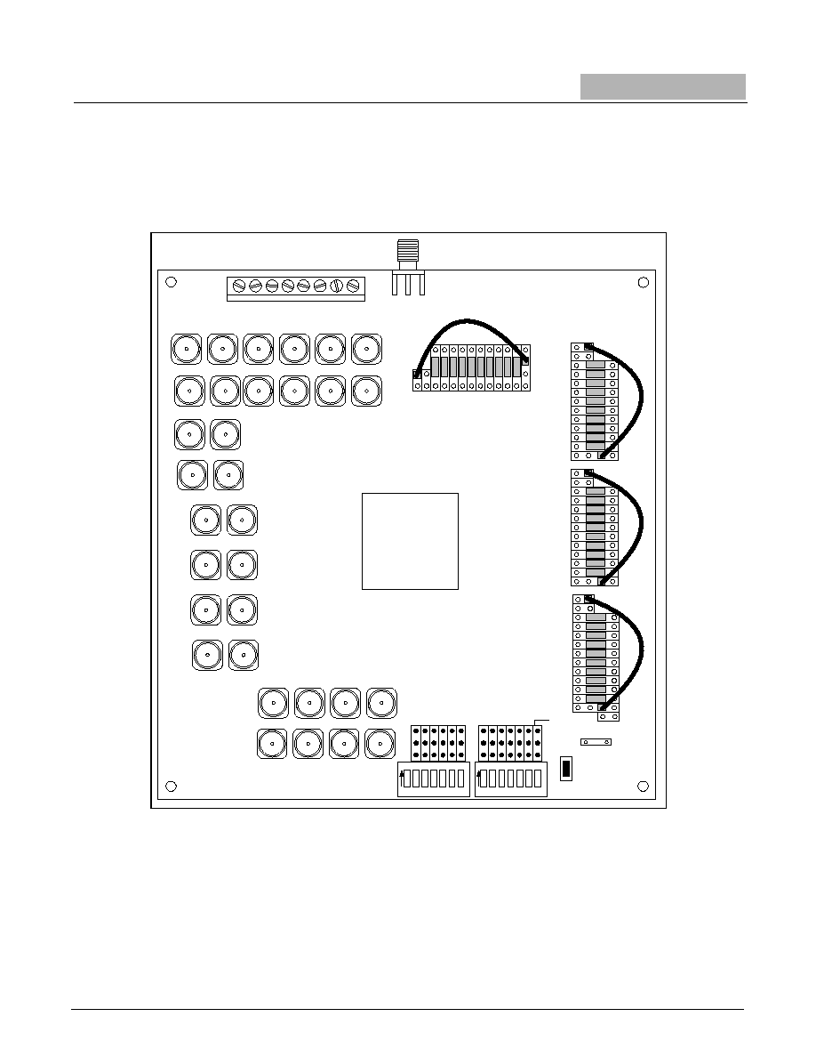
Test Setups
Typical tests performed with the S2065 evaluation board are Bit Error Rate Testing (BERT) and jitter testing. In
each case it is easiest to configure the evaluation board for serial input/output, looping back the parallel input/out-
put with jumpers. The serial input/output (parallel loopback) configuration is shown in Figure 2 and is described
below.
DIP switch settings for parallel loopback:
RESET
HIGH
LPEN
LOW
RATE
HIGH or LOW (determined by desired serial data rate)
MODE-10
Do not connect
TMODE
HIGH
CLKSEL
HIGH or LOW (determined by desired reference clock rate)
RXSELD
HIGH or LOW (determined by desired input)
RXSELC
HIGH or LOW (determined by desired input)
RXSELB
HIGH or LOW (determined by desired input)
RXSELA
HIGH or LOW (determined by desired input)
LC_BYP
Do not connect
CMODE
HIGH
CH_LOCK
LOW
Table 2. DIP Switch 2 Settings
DIP Name
Description
RXSELD
Channel D Input Select Control. Low selects input RX1D, High selects RX2D. (Internal
pull-up when not connected).
RXSELC
Channel C Input Select Control. Low selects input RX1C, High selects RX2C. (Internal
pull-up when not connected).
RXSELB
Channel B Input Select Control. Low selects input RX1B, High selects RX2B. (Internal
pull-up when not connected).
RXSELA
Channel A Input Select Control. Low selects input RX1A, High selects RX2A. (Internal
pull-up when not connected).
LC_BYP
Test signal. Not connected.
CMODE
Clock Mode Control for receiver data stream. When Low, the rate of the parallel output
clock (RCxP/N) is 1/2 the data rate, for ping/pong clocking. When High, the rate of the
parallel output clock (RCxP/N) is equal to the data rate.
CH_LOCK
Channel Lock Mode Control. Parallel input mode control. When High, locks all four
channels together. (See S2065 data sheet). When Low, provides independent channel
operation.
4
AMCC Confidential and Proprietary
EV2065 ≠ Quad Serial Backplane Device
with Dual I/O
EVALUATION BOARD
Revision 1.0 - November 18, 1999
In order to configure the board for parallel loopback, the parallel input data must be clocked into the device with the
TCLKx input clocks as shown in Figure 2. This clock is provided by looping the RCxP output clock back into the
respective TCLKx input with one of the minicoax cables provided in the EV2065 Kit. These cables need only be
connected for the channel(s) under test.
Figure 2. Parallel Loopback Configuration
REFCLK
AMCC
S2065
GND
RCCP
RCCN
ERRC
KFLAGC
DOUTC7
DOUTC6
DOUTC5
DOUTC4
DOUTC3
DOUTC2
DOUTC1
DOUTC0
EOFC
SOFC
KGENC
DINC7
DINC6
DINC5
DINC4
DINC3
DINC2
DINC1
DINC0
TCLKC
SOFB
KGENB
DINB7
DINB6
DINB5
DINB4
DINB3
DINB2
DINB1
DINB0
TCLKB
RCBP
RCBN
ERRB
KFLAGB
DOUTB7
DOUTB6
DOUTB5
DOUTB4
DOUTB3
DOUTB2
DOUTB1
DOUTB0
EOFB
SOFA
KGENA
DINA7
DINA6
DINA5
DINA4
DINA3
DINA2
DINA1
DINA0
TCLKA
TCLK0
RCAP
RCAN
ERRA
KFLAGA
DOUTA7
DOUTA6
DOUTA5
DOUTA4
DOUTA3
DOUTA2
DOUTA1
DOUTA0
EOFA
GND
GND
INPUT
OUTPUT
RCDP
RCDN
ERRD
KFLAGD
DOUTD7
DOUTD6
DOUTD5
DOUTD4
DOUTD3
DOUTD2
DOUTD1
DOUTD0
EOFD
SOFD
KGEND
DIND7
DIND6
DIND5
DIND4
DIND3
DIND2
DIND1
DIND0
TCLKD
GND
GND
O/P
I/P
GND
RX
VDDA
TX
VDD
RX
VDD
PECL
VDD
DIG
VDD
GND
TTL
VDD
AMCC
S2065 Evaluation Board
RX2CP
RX1CN
RX1DP
RX2DP
TX1AN
TX1AP
TX1BP
TX1BN
TX2AN
TX2AP
TX1CN
TX1CP
RESET
TX1DN
TX2BP
TX2CN
TX2DP
TX1DP
TX2BN
TX2CP
TX2DN
RX2DN
RX1DN
RX1CP
RX2CN
RESET
LPEN
RATE
MODE-10
TMODE
CLKSEL
RXSELD
RXSELC
RXSELB
RXSELA
LC BYP
CMODE
CH_LOCK
1 2 3 4 5 6 7
ON
1 2 3 4 5 6 7
ON
GND
RX2BP
RX1BP
RX1AN
RX2AN
RX2BN
RX1BN
RX1AP
RX2AP
AMCC Confidential and Proprietary
5
EV2065 ≠ Quad Serial Backplane Device
with Dual I/O
EVALUATION BOARD
Revision 1.0 - November 18, 1999
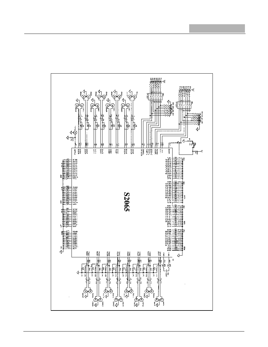
Schematic / Bill 0f Materials
Figures 3 and 4 provide a schematic representation of the EV2065 evaluation board. The bill of materials are out-
lined in Tables 3 and 4.
Figure 3. EV2065 Schematic