 | –≠–ª–µ–∫—Ç—Ä–æ–Ω–Ω—ã–π –∫–æ–º–ø–æ–Ω–µ–Ω—Ç: EV3050 | –°–∫–∞—á–∞—Ç—å:  PDF PDF  ZIP ZIP |
1
EV3050
OC-48 CLOCK RECOVERY UNIT EVALUATION BOARD
July 8, 1999
EV3050
Æ
OC-48 CLOCK RECOVERY UNIT EVALUATION BOARD
DESCRIPTION
The S3050 Evaluation Board provides a flexible plat-
form for verifying the operation of AMCC OC-48
clock recovery units. This document provides infor-
mation on the board's contents and layout. It should
be used in conjuction with the S3050 data sheet,
which contains full technical details on chip opera-
tion.
The S3050 board is factory configured with the
S3050 device, and includes a test point to monitor
the LOCKDET output. The board is configured for
use with an external oscillator connected to the
REFCLKP/N connectors.
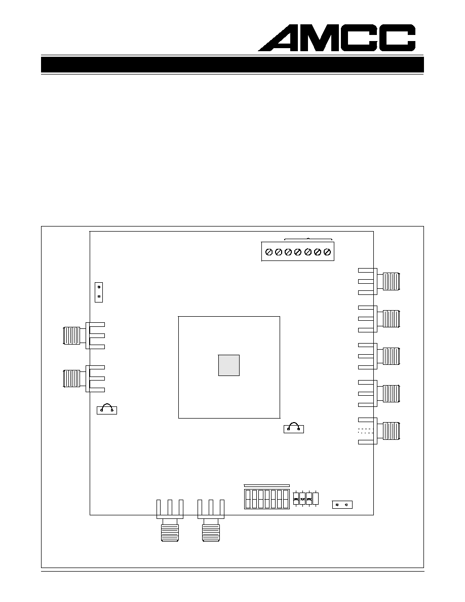
Power Connections
Terminal posts are provided at the top edge of the
board allowing separate control of voltage levels for
the S3050 itself. For operation with standard test
equipment, the board should be operated below
ground, with the VEE supply at -5V DC.
Figure 1. Board Layout
REFCLKP*
AMCC
S3050
GND
VEE7
AMCC
6290 SEQUENCE DRIVE
SAN DIEGO, CA 92121
S3050 MULTI-RATE
SONET/SDH CRU
SERCLKOP
SERCLKON
SERDATOP
SERDATON
VCOD32**
LOCKDET
GND
REFCLKN*
GND
GND
SERDATIP
SERDATIN
TESTSIG (TESTEN)
GND
BYPASS
LCKREFN
SDN
OFF ON
2 3 4
1
RESET
6 7
5
RATESEL1
RATESEL0
NC
R
Used for internal purposes
ELECTRICAL CONNECTIONS
* REFCLKP is labled as REFCLKN and REFCLKN is labled as REFCLKP on this board.
** VCOD32 is for internal use only.
2
EV3050
OC-48 CLOCK RECOVERY UNIT EVALUATION BOARD
July 8, 1999
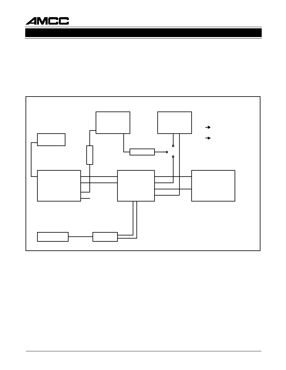
SET-UP FOR JITTER MEASUREMENT
Figure 2 depicts how the S3050 Evaluation Board can be connected for Jitter measurements and shows all of
the DIP switch settings and power supply requirements. The connection from A to B will be used for the PK-PK
edge/PK-PK Jitter on the DSO (Digital Storage Oscilloscope). The connection from A to C will be used for Jitter
Transfer, Jitter Tolerance and Jitter Generation measurement on the Transition Analyzer.
HP 70841B
B.E.R.T.
Tx (2.488 GHz)
S3050
HP 70842B
B.E.R.T.
Rx (2.488 GHz)
HP 70820A
Transition Analyzer
Tek CSA 803
D.S.O.
HP 3325
HP 8624B
BUFFER
SERDATIP
SERDATIN
CLK P
CLK N
MODULATION
INPUT
INPUT : 2
INPUT : 1
HP pn# 0955-0731
HP pn# 0955-0731
SERCLKOP
SERCLKON
SERDATOP
SERDATON
REFCLK
155.52 MHz
A
B
C
REFCLKP
REFCLKN
MAIN SIGNAL
CONNECTION
MEASUREMENT
A B :
PK-PK JITTER
A C :
JITTER TRANSFER
JITTER TOLERANCE
JITTER GENERATION
SWITCH
RATESEL "0"
RATESEL "1"
RESET
BYPASS
SDN
LCKREFN
#
2
3
4
5
7
6
HI (0V)
SEE TABLE 1
SEE TABLE 1
RESETS DATA
VCO/OFF
DATA OUT/OFF
LCK/DATA
LO (-5.0V)
SEE TABLE 1
SEE TABLE 1
NORMAL = LO
VCO/ON = LO
DATA OUT/ON = LO
LCK/REF = HI
POWER
VCC=GND :0V
VEE : -5.0V
Bandpass filter
2.488 GHz
Bandpass filter
2.488 GHz
(Note 2)
(Note 1)
Figure 2. Jitter Measurement Setup
Notes:
1. Edge Jitter is measured on SERDATON edge with data eye.
2. Can go single-ended with REFCLK at 200 mW (REFCLKP) and REFCLKN terminated with 50
to ground.
Make sure that the cables to BERT (SERCLK/SERDAT) are of equal length (EXACT). Different lengths will create bit errors. (When
measuring, cables of signals under test must be of equal length.)

3
EV3050
OC-48 CLOCK RECOVERY UNIT EVALUATION BOARD
July 8, 1999
y
l
p
p
u
S
r
e
w
o
P
t
u
p
n
I
l
a
n
i
m
o
N
e
g
a
t
l
o
V
l
a
n
g
i
S
f
o
e
p
y
T
t
u
p
t
u
O
L
M
C
n
o
i
t
a
n
i
m
r
e
T
C
C
V
T
U
D
E
E
V
T
U
D
V
0
V
0
.
5
-
L
C
E
=
t
u
p
n
I
L
M
C
=
t
u
p
t
u
O
0
5
D
N
G
o
t
Table 1. Power Connections for DUT and Test Equipment Interface
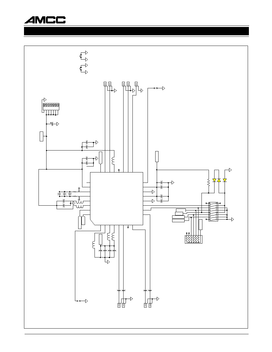
SMA Connectors
SMA connectors are provided for the differential serial data input/output signals and output clock. Cables to
these connectors must be the same length.
Serial Data In [SERDATIP/N] ≠ ECL Differential inputs. Serial Data In. Clock is recovered from the transitions
on these inputs.
Reference Clock [REFCLKP/N] ≠ ECL Differential inputs. These inputs are used to establish the initial operat-
ing frequency of the clock recovery PLL and also used as a standby clock in the absence of data. These inputs
must be provided with a differential clock of 155.52 MHz. (AC Coupled).
Serial Data Out [SERDATOP/N] ≠ CML outputs. This signal is the delayed version of the incoming data stream
(SERDATI) updated on the falling edge of Serial Clock Out (SERCLKOP).
Serial Clock Output [SERCLKOP/N] ≠ CML outputs. This signal is phase aligned with Serial Data Out
(SERDATOP).
Jumper
Lock Detect [LOCKDET] -- TTL output. Indicates that the Clock Recovery has locked onto the incoming data
stream.
Dip Switches
The Evaluation Board is equipped with a DIP switch to control the static control functions of the on-board
devices. For both arrays the OFF (open = "0") condition of the DIP switch asserts a logic low on the assigned
signal, and the ON (closed = "1") condition asserts a Logic High. Figure 2 shows the DIP switch settings needed
for a particular test case. (Should show Logic "1" or Logic "0").
4
EV3050
OC-48 CLOCK RECOVERY UNIT EVALUATION BOARD
July 8, 1999
Figure 3. Schematic
C14
0.1uF
C15
0.1uF
C16
0.1uF
SERDA
TIP
J4
SERDA
TIN
J5
REFCLKP
J9
REFCLKN
J10
C17
0.1uF
23
SERCLKOP
22
SERCLKON
21
A
VEE
19
SERDA
T
O
P
18
SERDA
T
O
N
17
VCODIV32
25
26
27
28
29
30
2
A
VCC
3
A
VEE
4
A
VEE
5
SERDA
TIP
6
SERDA
TIN
1
TESTEN
7
NC
8
REFCLKP
11
SDN
12
VCC
13
VEE
14
VCC
15
VEE
9
REFCLKN
10
LCKREFN
16
LOCKDET
20
NC
24
24
150K
150K
24
RA
TESEL1
32
31
S3050
U1
C18
100pF
C19
0.1uF
C20
100pF
3050VEE
1N4148
D1
D2
1N4148
D3
1N4148
R3
1K
R4
1K
SW1
BYPASS
3050VEE
RATESEL1
RESET
RATESEL0
OPEN ="0"
CLOSED ="1"
TESTEN
JP1
L3
3
C13
0.1uF
C12
100pF
C1
1
0.1uF
C10
100pF
C9
0.1uF
10
µ
F
10
µ
F
2.2
µ
F
C6
100pF
C5
0.1uF
C4
100pF
C3
0.1uF
L6
L5
L4
L2
L1
RA
TESEL0
RESET
RA
TESEL1
3050VEE
JP3
JP4
1
2
3
4
5
6
7
J1
GND
LOOPS
C7
0.1uF
C8
100pF
3050VEE
C2
10uF
SERCLKOP
J2
SERCLKON
J3
JP2
LOCKDET
SERDA
T
O
P
J6
SERDA
T
O
N
J7
VCOD32
J8
VCC
VEE
CAP2
CAP1
AVCC
AVEE
RESET
RATESEL0
6
11
10
9
8
7
15
1
3
2
14
16
5
4
13
12
3
4
1
2
5
6
7
*
*
* subject to change
5
EV3050
OC-48 CLOCK RECOVERY UNIT EVALUATION BOARD
July 8, 1999
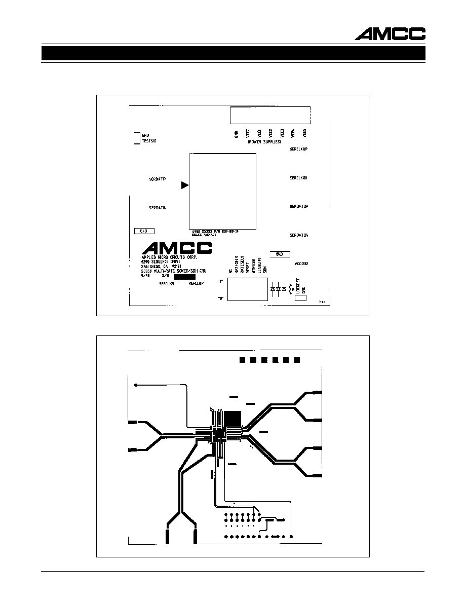
Figures 4 through 9 show the layout of the S3050 Evaluation Board.
Figure 4.
Figure 5.