 | –≠–ª–µ–∫—Ç—Ä–æ–Ω–Ω—ã–π –∫–æ–º–ø–æ–Ω–µ–Ω—Ç: S2018 | –°–∫–∞—á–∞—Ç—å:  PDF PDF  ZIP ZIP |
1
S2018
17 X 17 3.2 GBIT/S DIFFERENTIAL CROSSPOINT SWITCH
July 25, 2000 / Revision D
S2018
Æ
17 X 17 3.2 GBIT/S DIFFERENTIAL CROSSPOINT SWITCH
DEVICE
SPECIFICATION
FEATURES
∑ SiGe BiCMOS Technology
∑ 17 x 17 differential crosspoint switch
∑ Broadcast and multicast switching capability
∑ Differential 200 mV to 1400 mV input data
∑ Differential 200 mV to 1300 mV
programmable output swing
∑ Up to 3.2 Gbps NRZ data rate
∑ LVTTL configuration controls
∑ Internal 100
line-to-line terminations on high-
speed differential inputs
∑ Reconfigurable without disturbing operation
∑ 35 mm x 35 mm 352 pin SBGA package
∑ +3.3 V only power supply
∑ 4 W typical power dissipation with
800 mV output swing
∑ Complies with Bellcore and ITU-T Standard
APPLICATIONS
∑ Dense Wavelength Division Multiplexing
(DWDM) systems
∑ Internet switches
∑ Digital video
∑ Digital demultiplexing
∑ Microwave or fiber-optic data distribution
∑ High-speed automatic test equipment
∑ Datacom or telecom switching
GENERAL DESCRIPTION
The S2018 is a high speed 17 x 17 differential cross-
point switch with full broadcast capability. Any of its
17 differential LVPECL input signal pairs can be con-
nected to any or all of its 17 differential CML output
signal pairs.
The differential 10K LVPECL logic data path makes
the part ideal for high-speed applications. The differ-
ential nature of the data path is retained throughout
the crosspoint structure to minimize data distortion
and to handle NRZ data rates up to 3.2 gigabits per
second. The high-speed serial inputs to the S2018
are internally biased and have internal 100
line-to-
line terminations.
LVTTL configuration controls simplify interfacing to
slower speed circuitry. Once a new configuration has
been entered into the configuration register file, the
S2018 can be completely reconfigured by pulsing
the CONFIGN input.
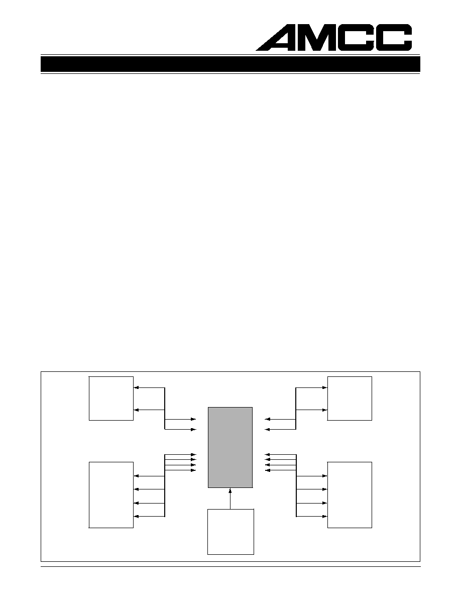
Figure 1 shows a system block diagram incorporat-
ing the S2018 with AMCC serial backplane devices.
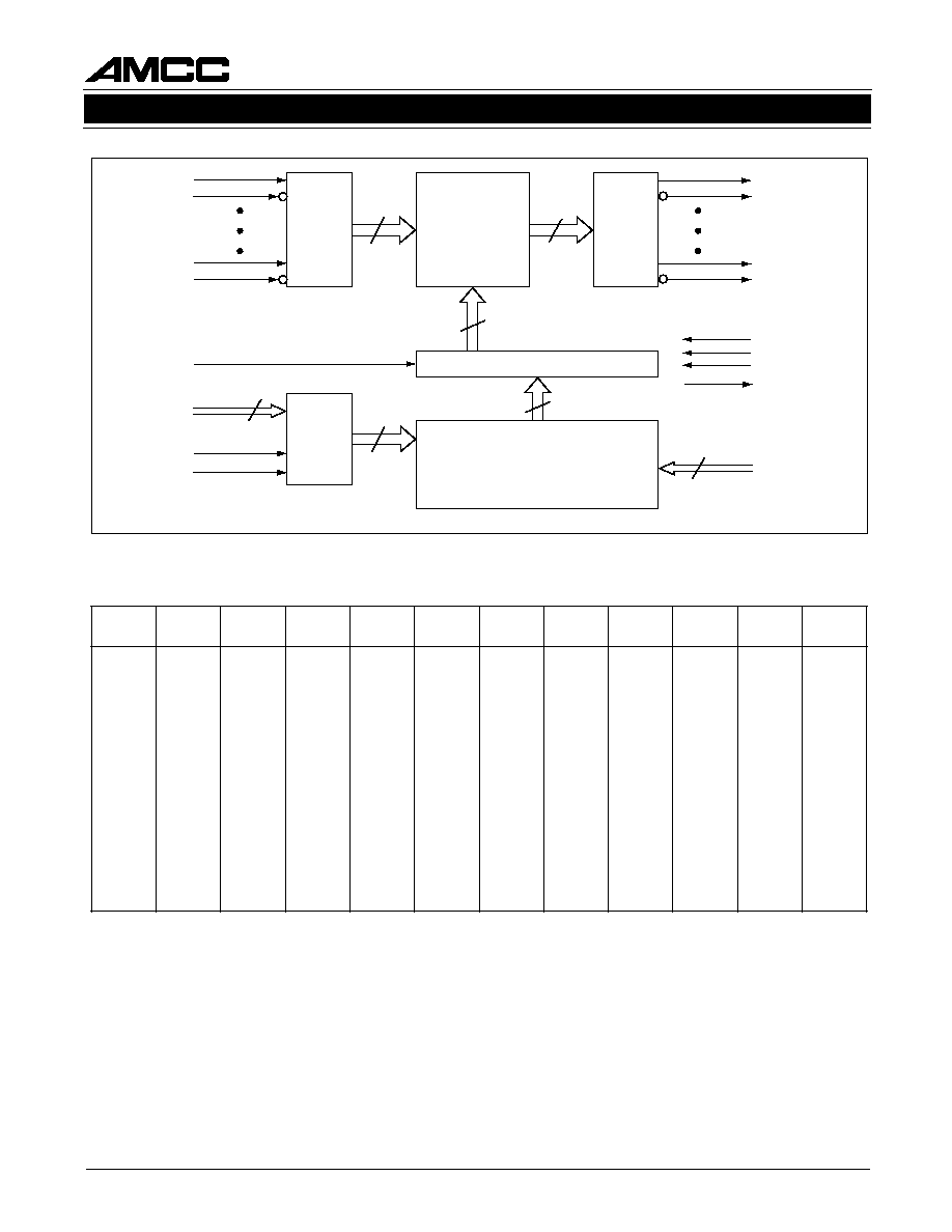
Figure 2 shows the basic operation of the switch.
Figure 1. System Block Diagram
.
.
.
.
.
.
.
.
16
0
S2062
S2004
.
.
.
.
.
.
.
.
0
16
S2064
S2002
S2018
Crosspoint
Switch
Crosspoint
Control
(
µ
P &
DRAM)
2
S2018
17 X 17 3.2 GBIT/S DIFFERENTIAL CROSSPOINT SWITCH
July 25, 2000 / Revision D
Figure 2. Functional Block Diagram
Diff.
LVPECL
Input
Buffers
Diff.
CML
Output
Buffers
17 x 17
Differential
Crosspoint
34
34
DIN0P
DIN16P
DOUT0P
DOUT16P
Active Configuration Latch
85
17 x 5
Configuration
Register File
85
IADDR[4:0]
DATA
17
5:17
Decode
EN
CONFIGN
LOADN
CSN
OADDR[4:0]
5
5
SELECT
DOUT0N
DOUT16N
DIN0N
DIN16N
VADJUST3
VADJUST2
VADJUST1
VCSHIGH
F
F
I
D
T
U
P
N
I
4
R
D
D
A
I
3
R
D
D
A
I
2
R
D
D
A
I
1
R
D
D
A
I
0
R
D
D
A
I
F
F
I
D
T
U
P
T
U
O
4
R
D
D
A
O
3
R
D
D
A
O
2
R
D
D
A
O
1
R
D
D
A
O
0
R
D
D
A
O
0
N
I
D
1
N
I
D
2
N
I
D
3
N
I
D
4
N
I
D
5
N
I
D
6
N
I
D
7
N
I
D
8
N
I
D
9
N
I
D
0
1
N
I
D
1
1
N
I
D
2
1
N
I
D
3
1
N
I
D
4
1
N
I
D
5
1
N
I
D
6
1
N
I
D
0
0
0
0
0
0
0
0
0
0
0
0
0
0
0
0
1
0
0
0
0
0
0
0
0
1
1
1
1
1
1
1
1
X
0
0
0
0
1
1
1
1
0
0
0
0
1
1
1
1
X
0
0
1
1
0
0
1
1
0
0
1
1
0
0
1
1
X
0
1
0
1
0
1
0
1
0
1
0
1
0
1
0
1
X
0
T
U
O
D
1
T
U
O
D
2
T
U
O
D
3
T
U
O
D
4
T
U
O
D
5
T
U
O
D
6
T
U
O
D
7
T
U
O
D
8
T
U
O
D
9
T
U
O
D
0
1
T
U
O
D
1
1
T
U
O
D
2
1
T
U
O
D
3
1
T
U
O
D
4
1
T
U
O
D
5
1
T
U
O
D
6
1
T
U
O
D
0
0
0
0
0
0
0
0
0
0
0
0
0
0
0
0
1
0
0
0
0
0
0
0
0
1
1
1
1
1
1
1
1
X
0
0
0
0
1
1
1
1
0
0
0
0
1
1
1
1
X
0
0
1
1
0
0
1
1
0
0
1
1
0
0
1
1
X
0
1
0
1
0
1
0
1
0
1
0
1
0
1
0
1
X
Table 1. Input/Output Address of S2018
Note: X denotes don't care
3
S2018
17 X 17 3.2 GBIT/S DIFFERENTIAL CROSSPOINT SWITCH
July 25, 2000 / Revision D
DATA TRANSFER
For each configured connection between a differen-
tial input pair and an enabled output pair, any data
appearing at the input pair will be passed immedi-
ately through to the output pair.
CONFIGURATION
The S2018 can be selectively configured one output
pair at a time, or any number of output pairs simulta-
neously. Configuration data is stored in 17 registers,
one register for each output pair. The data in these
17 configurations register makes up the configura-
tion register file. As shown in Figure 2, the configura-
tion data is passed in parallel from all 17 registers to
a latch, which holds the active switch configuration.
This two-stage arrangement allows one or more out-
put pairs to be configured simultaneously. A Chip
Select pin (CSN) is provided to simplify interfacing
this switch to the system microprocessor.
The S2018 minimizes the configuration time through
the use of the active configuration latch. While the
switch is operational, and prior to the time at which it
must be reconfigured, a new configuration is loaded
into the configuration register file. Once the configu-
ration register file contains the desired connection
information, the contents of the registers are trans-
ferred in parallel to the active configuration latch by
the CONFIGN strobe.
To connect an output to a given input, the output to
be configured is selected using the OADDR[4:0]
(OADDR4=MSB) inputs. See Table 1. With the out-
put configuration register selected, the desired input
selection must be provided in the IADDR[4:0]
(IADDR4=MSB) inputs. The IADDR[4:0] information
is stored into the selected output configuration regis-
ter by the LOADN strobe. The configuration process
is described by the flow chart in Figure 5.
The active configuration latch can be made transpar-
ent by activating the CONFIGN input. When this is
done, changes strobed into the output pair configu-
ration registers by the LOADN input pair will be
passed immediately to the switch.
The S2018 supports both broadcast and multicast
operation: any of the 17 differential input pairs can
be connected to any or all of the 17 differential out-
put pairs.
OUTPUT SWING ADJUST
The S2018 output swing can be adjusted by con-
necting one or more of the VADJUSTx pins to the
VCSHIGH pin according to Table 2. Note that as the
output swing is increased, the power dissipated by
the part is proportionally increased (See Table 10).
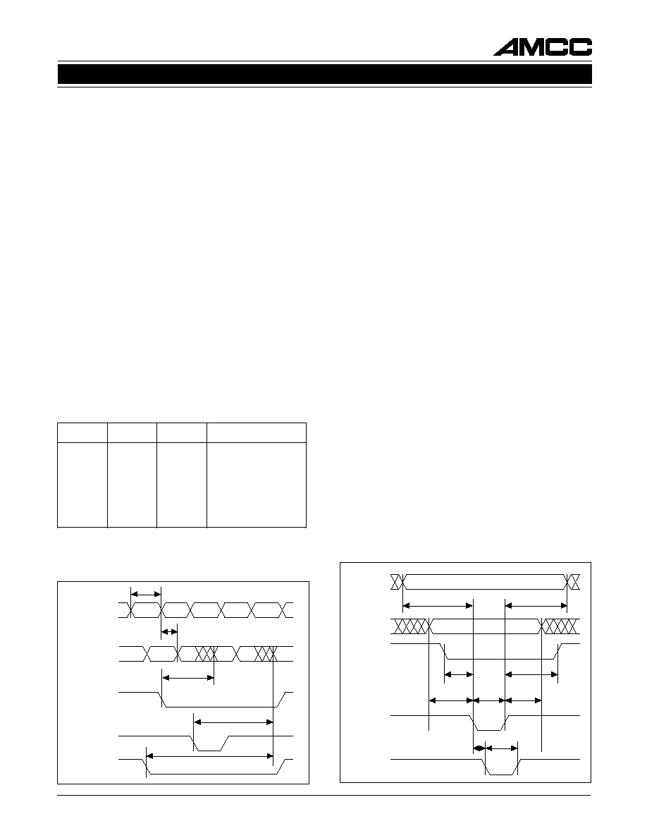
Figure 3. Data Transfer Waveforms
Figure 4. Reconfiguration Waveforms
1
t
s
u
j
d
a
V
2
t
s
u
j
d
a
V
3
t
s
u
j
d
a
V
)
.
f
f
i
D
p
p
V
m
(
x
x
T
U
O
D
T
O
T
O
T
O
T
O
T
T
O
O
T
T
O
O
O
T
T
T
T
0
4
2
0
4
4
0
0
6
0
8
7
0
4
9
0
0
1
1
0
6
2
1
Table 2. Output Swing Adjust Pin Settings
Note: T = Ties pin(s) VADJUSTx to pin VCSHIGH
O = Open
tCFDO
tLDDO
tDIDO
DIMPW
DIN[16:0]P/N
DOUT[16:0]P/N
CONFIGN
CSN
LOADN
A
A
B
C
D
E
B
C
D
E
tCSDO
tSUIA
LDMPW
tHIA
tSULC
CFMPW
tSUOA
tHOA
OADDR[4:0]
IADDR[4:0]
CSN
LOADN
VALID
VALID
CONFIGN
tSUCS
tHCS
4
S2018
17 X 17 3.2 GBIT/S DIFFERENTIAL CROSSPOINT SWITCH
July 25, 2000 / Revision D
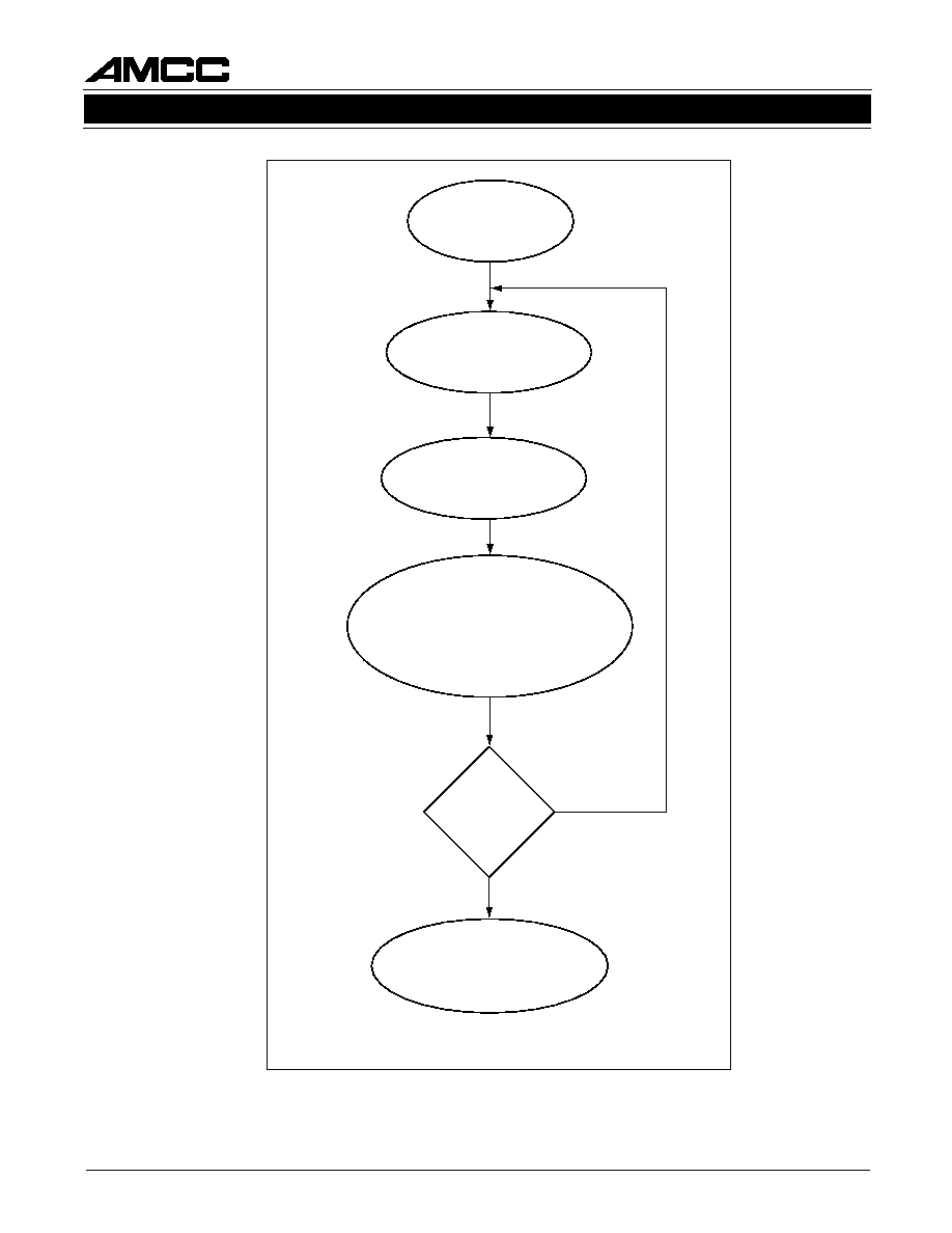
Activate
CSN
Configure OADDR[4:0]
to desired output.
See Table 1.
Configure IADDR[4:0]
to desired input.
See Table 1.
Strobe LOADN
to store the input address (IADDR[4:0])
in the section of the Configuration
Register File pointed to by the
output register (OADDR[4:0])
Configure
another
output?
Strobe CONFIGN
to store all connections to the
Active Configuration Latch
YES
NO
Figure 5. S2018 Configuration Flow Chart

5
S2018
17 X 17 3.2 GBIT/S DIFFERENTIAL CROSSPOINT SWITCH
July 25, 2000 / Revision D
Table 3. Data Transfer Timing
1,2
r
e
t
e
m
a
r
a
P
n
o
i
t
p
i
r
c
s
e
D
n
i
M
p
y
T
x
a
M
s
t
i
n
U
s
n
o
i
t
i
d
n
o
C
t
O
D
I
D
N
/
P
]
0
:
6
1
[
N
I
D
m
o
r
f
y
a
l
e
d
n
o
i
t
a
g
a
p
o
r
P
N
/
P
]
0
:
6
1
[
T
U
O
D
o
t
5
.
1
s
n
t
O
D
F
C
f
o
e
g
d
e
g
n
il
l
a
f
m
o
r
f
y
a
l
e
d
n
o
i
t
a
g
a
p
o
r
P
d
il
a
v
N
/
P
]
0
:
6
1
[
T
U
O
D
o
t
N
G
I
F
N
O
C
3
s
n
t
O
D
D
L
f
o
e
g
d
e
g
n
il
l
a
f
m
o
r
f
y
a
l
e
d
n
o
i
t
a
g
a
p
o
r
P
d
il
a
v
N
/
P
]
0
:
6
1
[
T
U
O
D
o
t
N
D
A
O
L
)
w
o
L
d
l
e
h
s
i
N
G
I
F
N
O
C
n
e
h
w
(
4
s
n
t
O
D
S
C
f
o
e
g
d
e
g
n
il
l
a
f
m
o
r
f
y
a
l
e
d
n
o
i
t
a
g
a
p
o
r
P
n
e
h
w
(
d
il
a
v
N
/
P
]
0
:
6
1
[
T
U
O
D
o
t
N
S
C
)
w
o
L
d
l
e
h
s
i
N
G
I
F
N
O
C
0
1
s
n
I
D
W
P
M
N
/
P
]
0
:
5
1
[
N
I
D
f
o
h
t
d
i
w
e
s
l
u
P
0
8
2
s
p
6
1
I
D
W
P
M
N
/
P
6
1
N
I
D
f
o
h
t
d
i
w
e
s
l
u
P
0
9
s
p
F
X
A
M
e
t
a
R
a
t
a
D
2
.
3
s
p
b
G
T
S
M
R
r
e
t
t
ij
t
u
p
n
i
y
n
a
,
n
o
i
t
a
l
u
m
u
c
c
a
r
e
t
t
ij
m
o
d
n
a
R
:
t
a
t
u
p
t
u
o
y
n
a
o
t
s
p
b
G
2
.
3
s
p
b
G
5
.
2
s
p
b
G
5
.
1
9
.
1
9
.
1
9
.
1
3
3
3
s
p
r
e
t
t
ij
t
u
p
t
u
o
S
M
R
h
t
i
w
d
e
t
a
l
u
m
u
c
c
a
n
o
d
e
t
s
e
T
.
e
d
o
c
7
.
8
2
K
.
s
i
s
a
b
e
l
p
m
a
s
a
T
r
e
t
t
ij
J
D
y
n
a
,
n
o
i
t
a
l
u
m
u
c
c
a
r
e
t
t
ij
c
i
t
s
i
n
i
m
r
e
t
e
D
:
t
u
p
t
u
o
y
n
a
o
t
t
u
p
n
i
s
p
b
G
2
.
3
s
p
b
G
5
.
2
s
p
b
G
5
.
1
9
1
8
1
8
1
7
2
7
2
7
2
s
p
t
u
p
t
u
o
c
i
t
s
i
n
i
m
r
e
t
e
D
d
e
t
a
l
u
m
u
c
c
a
r
e
t
t
ij
d
e
t
s
e
T
.
n
r
e
t
t
a
p
5
.
8
2
K
.
s
i
s
a
b
e
l
p
m
a
s
a
n
o
.
k
a
e
p
-
o
t
-
k
a
e
P
e
n
o
w
e
k
S
m
o
r
f
s
h
t
a
p
n
e
e
w
t
e
b
w
e
k
s
t
s
a
c
d
a
o
r
B
e
l
p
i
t
l
u
m
o
t
)
]
0
:
5
1
[
N
I
D
(
t
u
p
n
i
e
n
o
y
n
a
s
e
d
u
l
c
x
E
.
)
]
0
:
5
1
[
T
U
O
D
(
s
t
u
p
t
u
o
.
]
6
1
[
T
U
O
D
d
n
a
]
6
1
[
N
I
D
0
4
1
s
p
ll
a
w
e
k
S
e
l
p
i
t
l
u
m
m
o
r
f
s
h
t
a
p
n
e
e
w
t
e
b
w
e
k
S
s
t
u
p
t
u
o
e
l
p
i
t
l
u
m
o
t
)
]
0
:
5
1
[
N
I
D
(
s
t
u
p
n
i
d
n
a
]
6
1
[
N
I
D
s
e
d
u
l
c
x
E
.
)
]
0
:
5
1
[
T
U
O
D
(
.
]
6
1
[
T
U
O
D
0
5
1
s
p
6
1
e
n
o
w
e
k
S
m
o
r
f
s
h
t
a
p
n
e
e
w
t
e
b
w
e
k
s
t
s
a
c
d
a
o
r
B
e
l
p
i
t
l
u
m
o
t
)
]
0
:
6
1
[
N
I
D
(
t
u
p
n
i
e
n
o
y
n
a
.
)
]
0
:
6
1
[
T
U
O
D
(
s
t
u
p
t
u
o
0
0
3
s
p
6
1
ll
a
w
e
k
S
e
l
p
i
t
l
u
m
m
o
r
f
s
h
t
a
p
n
e
e
w
t
e
b
w
e
k
S
s
t
u
p
t
u
o
e
l
p
i
t
l
u
m
o
t
)
]
0
:
6
1
[
N
I
D
(
s
t
u
p
n
i
.
)
]
0
:
6
1
[
T
U
O
D
(
0
6
4
s
p
T
r
T
,
f
)
%
0
8
o
t
%
0
2
(
e
t
a
R
e
g
d
E
t
u
p
t
u
O
5
2
1
s
p
0
0
1
.
e
n
il
-
o
t
-
e
n
il
1. All data transfer timing measured from the crossing point of the differential inputs to the crossing point of the differential outputs.
2. All data measured with 800 mVpp swing.