 | –≠–ª–µ–∫—Ç—Ä–æ–Ω–Ω—ã–π –∫–æ–º–ø–æ–Ω–µ–Ω—Ç: S2020B | –°–∫–∞—á–∞—Ç—å:  PDF PDF  ZIP ZIP |
1
S2020/S2021
HIPPI SOURCE/DESTINATION INTERFACE CIRCUITS
Æ
HIPPI SOURCE/DESTINATION INTERFACE CIRCUITS
S2020/S2021
FEATURES
∑ Functionally compliant with the ANSI HIPPI
standard
∑ 32-Bit data channel
∑ Equivalent single channel rate of 800 Mbits/sec
∑ Host-side interface single-ended TTL designed
for use with external FIFO
∑ Channel-side interface differential ECL 10K
∑ Four rank data and control signal
synchronization
∑ Byte parity checking
∑ Length/Longitudinal Redundancy Checkword
(LLRC) generation and checking
∑ Automatic division of data into HIPPI bursts
∑ 16-Bit READY counter for flow control
∑ Maximum latency through both ICs
Connection: 600ns, Data: 400ns
∑ Diagnostic modes for self test
∑ Standard +5V, 0V(gnd), and -5.2V power
requirements
∑ 225-pin ceramic PGA package
∑ 208-pin Thermally Enhanced Plastic (TEP)
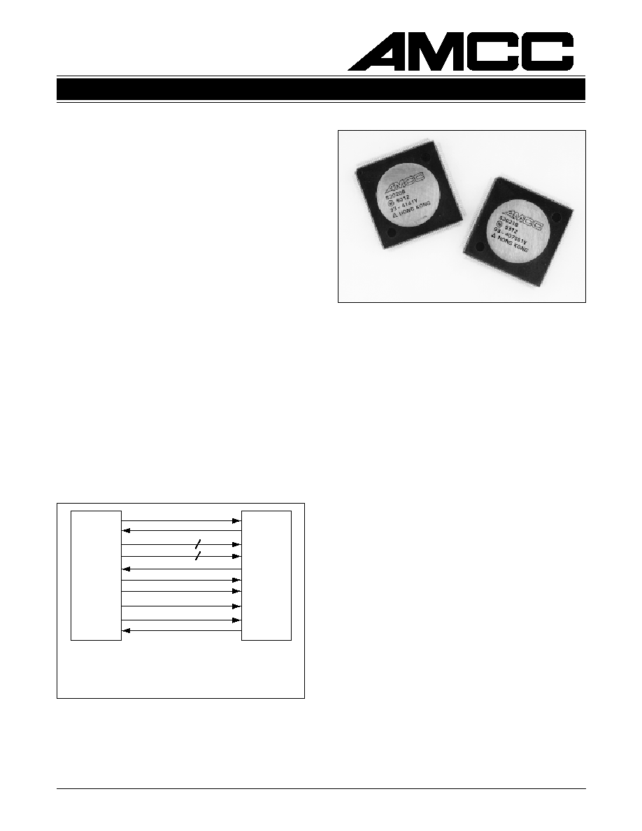
S2020/S2021 HIPPI Chipset
Figure 1. Interface Signal Summary
GENERAL DESCRIPTION
The S2020 and the S2021 are Source and Destination
interface circuits, respectively, for the High-
Performance Parallel Interface (HIPPI) standard.
These circuits are designed to completely meet the
signalling protocol of the proposed ANSI HIPPI
specification: current document number X3.183≠
1991 They include both LLRC generation and
checking as well as byte parity checking. The
S2021 also incorporates a sophisticated four rank
synchronization scheme to ensure that the incoming
data and control signals are coupled to the local
clock. Data flow control is provided by a 16-bit ready
counter in both the Source and the Destination
circuits. HIPPI data BURST partitioning is also
provided in the Source circuit.
Architected and designed by Network Systems
Corporation, the S2020 and S2021 utilize AMCC's
1.5-micron BiCMOS technology. AMCC's BiCMOS
technology is especially optimized for high performance
mixed mode ECL/TTL applications such as the
HIPPI Source and Destination interfaces. AMCC
pioneered ECL/TTL mixed mode BiCMOS capability
and continues to be the leading U.S. supplier of
BiCMOS VLSI circuits.
Request
Connect
Data Bus
Parity Bus
Ready
Packet
Burst
Clock
Interconnect S
D
Interconnect D
S
Source: ANSI X3.183≠1991
High-Performance Parallel Interface.
Mechanical, Electrical, and Signalling
Protocol Specification (HIPPI-PH).
Source
Destination
32
4
DEVICE SPECIFICATION
2
S2020/S2021
HIPPI SOURCE/DESTINATION INTERFACE CIRCUITS
HIPPI OVERVIEW
The individual HIPPI channel is a simplex interface,
meaning that data moves in one direction from the
HIPPI Source (S2020) to the HIPPI Destination
(S2021). Thus a fully bidirectional interface requires
the use of two HIPPI channels as indicated in the
System Block Diagram.
Once the connection is established, data transfer
can proceed according to the Physical Framing
Hierarchy (see Figure 3). The basic data block is the
Burst consisting of from 1 to 256 words of 32 data
bits and 4 bits of odd byte parity. Each Burst is
delimited by the assertion and deassertion of the
BURST signal by the data Source. Every burst is
followed immediately by Length/Longitudinal Redun-
dancy Checkword (LLRC) which is the even parity
for each bit for the entire length of the Burst together
with the modulo 256 count of the number of words in
the Burst. The count is included in the parity
calculation for the least significant 8 bits of the LLRC
word. For the normal full burst of 256 words, the
count is all zeros (256 base 2 truncated to 8 bits).
Figure 2. System Block Diagram
Figure 3. Physical Framing Hierarchy
HOST
MEMORY
SYSTEM
FIFO
S
2
0
2
0
S
2
0
2
1
S
2
0
2
1
S
2
0
2
0
FIFO
FIFO
FIFO
HOST
MEMORY
SYSTEM
HIPPI
HIPPI
The transfer of data from the Source to the
Destination depends on the physical connection of
the two endpoints and the exchange of requesting,
acknowledging, and data delimiting signals. The
Source and Destination circuits both observe the
state of the INTERCONNECT signals to verify a
physically intact channel. If both Source and
Destination are interconnected, the Source may
initiate a data transfer by asserting the REQUEST
signal. At the same time the Source places a 32 bit
word also known as the I-Field on the data lines
together with the appropriate Byte parity. The Upper
Level Protocols (ULPs) controlling the Source and
Destination may use this information for routing. The
Destination responds to the REQUEST by asserting
the CONNECT signal either for a short period while
leaving the READY signal inactive to actively reject
the REQUEST, or by asserting CONNECT and then
asserting the READY signal to accept the REQUEST
and indicate the availability of an input data buffer.
The Destination can also accept the REQUEST by
asserting CONNECT for a longer period without
sending a READY, thus indicating a temporary delay
in the availability of an input data buffer. The Source
may remove the I-Field data after detecting the
CONNECT signal.
Disabled
Packet
Wait Burst LLRC Wait
Burst LLRC Wait
Burst LLRC
Packet
Wait
Packet
I-Field
Connection
256 words of 32 bits each
Source: ANSI X3.183≠1991
High-Performance Parallel Interface.
Mechanical, Electrical, and Signalling
Protocol Specification (HIPPI-PH).
One or more Bursts are grouped as a Packet
delimited by the assertion and deassertion of the
PACKET signal by the Source. Wait periods are
placed between Bursts and between Packets to
allow synchronization adjustments between the
Source and Destination circuits. A connection may
contain one or more Packets. The details of the data
transfer handshake are shown in Figure 4.
S2020 AND S2021 DESCRIPTION
The S2020 Source and the S2021 Destination
circuits generate all of the required control and
handshaking signals described above in the correct
timing relationships, as well as providing Burst and
Packet control, READY to BURST coordination, and
LLRC generation and checking.

3
S2020/S2021
HIPPI SOURCE/DESTINATION INTERFACE CIRCUITS
The circuits provide diagnostic modes for testing the
devices themselves plus the circuitry that interfaces
to the device. In the self-test modes, the INTER-
C O N N E C T s i g n a l c a n b e d e a s s e r t e d . T h i s
effectively "unplugs" the device undergoing self-test
from the HIPPI channel making it unavailable for
connection and thus unable to generate spurious data
or control information while in the diagnostic mode.
S2020 HIPPI SOURCE DEVICE
This device meets the signalling protocol requirements
for a HIPPI-Source; i.e., it controls the forward signals
and receives and acts on the reverse signals.
The Host-side consists of 45 single-ended TTL inputs
used for data, control and the 50 MHz clock as well
as 9 single-ended TTL outputs used for control of
the external FIFO and to obtain device status.
The HIPPI-side consists of 40 differential ECL
outputs (forward signals), 2 differential ECL inputs
(reverse signals), 1 single-ended TTL output
(Source-to-Destination INTERCONNECT signal) and
1 single-ended ECL input (Destination-to-Source
INTERCONNECT signal).
ELECTRICAL REQUIREMENTS
The differential ECL outputs require eighty 330 Ohm
2% resistors, one per pin. The differential ECL inputs
require two 110 Ohm 2% resistors, one per input pair.
The two INTERCONNECT signals require external
transmit and receive networks to reliably implement the
signal swing required by the HIPPI Specification. For
the Source-to-Destination INTERCONNECT (output
signal), the required network is shown in Figure 10.
It should be noted that this network is only required if
switching control of the INTERCONNECT signal by
the Source device is desired. The network may be
omitted and a simple pull-down of the Source-to-
Destination INTERCONNECT via a 220 Ohm resistor
to Vee may be used as indicated in the ANSI standard.
For the Destination-to-Source INTER-CONNECT (input
signal), the required network is shown in Figure 11.
The network is strongly recommended for use on the
received INTERCONNECT signal to avoid risk of
saturation when operated with a switchable INTER-
CONNECT Destination device such as the S2021. It
is also recommended for use in the non-switched
passive pull-down applications to avoid damage to the
ECL input due to transients caused by mechanical
connection/disconnection cycles of the allowed cabling
while Source and Destination are under power.
Figure 4. Typical HIPPI-PH Waveforms
The Host systems are the actual originator and the
ultimate destination of the data sent over the HIPPI
channel. The purpose of the S2020 and S2021 is to
decouple the Host hardware and software from the
timing and formatting details of the interface. Each
circuit can be considered as having a "Host-side"
and a "HIPPI-side." The Host-side of the Source
circuit accepts data from the Host FIFO and passes
it to the HIPPI-side. The HIPPI-side controls the
forward signals (REQUEST, PACKET, BURST and
CLOCK) and receives the reverse signals (CONNECT
and READY) of the HIPPI channel. The HIPPI-side of
the Destination circuit receives the forward signals
and controls the reverse signals of the HIPPI
channel. The Host-side of the Destination delivers
the received data to the Host FIFO.
The Host-side of both circuits can be thought of as
consisting of four sections:
∑ Connect Control (for connecting/disconnecting
to/from the HIPPI channel)
∑ Data/FIFO Control (for moving data to/from the
Host logic)
∑ Data + Parity (for presenting data to/from the
Host logic
∑ Status/Control (for general control of the circuit
and to obtain status from the circuit)
The purpose of these circuits is to reduce the
complexity of the circuitry required to mate a Host
memory system to the HIPPI channel. The Host-side
is primarily single-ended TTL while the HIPPI-side is
primarily differential ECL. Beside meeting the
signalling protocol requirements of the HIPPI
standard, the circuits provide a reduction of the
signal lines to the host interface.
I-Field
LLRC
Data
Burst
LLRC
Data
Burst
LLRC
Data
Burst
REQUEST (S)
CONNECT(D)
READY (D)
PACKET (S)
BURST (S)
DATA BUS (S)
Source: ANSI X3.183≠1991
High-Performance Parallel Interface.
Mechanical, Electrical, and Signalling
Protocol Specification (HIPPI-PH).

4
S2020/S2021
HIPPI SOURCE/DESTINATION INTERFACE CIRCUITS
CONNECTION LATENCY
The Connection latency through the Source device
consists of two parts: 1) The delay from the rising
edge of the TTL input CONNECT_REQUEST to the
assertion of the REQUEST signal in parallel with the
placement of the I-Field data on the Host data bus
and its availability on the HIPPI channel data bus (4
clock cycles), and 2) the delay from the detection of
the CONNECT signal for the 17th clock cycle and
the assertion of the TTL outputs CONNECT_OUT
and ACCEPT/REJECT to the Host (3 to 4 clock
cycles). The total connection latency in the Source
device ranges from 7 to 8 clock cycles. This does
not include cable delay or Destination processing.
DATA LATENCY
The data latency through the Source device is
defined as the delay from the rising edge of the
BURST_AVAILABLE signal and the assertion of the
BURST signal on the HIPPI channel. The data
latency is 4 clock cycles. This does not include cable
delay or Destination processing.
SOURCE CONNECT CONTROL
Connection control is provided by four control signals
and two error flags on the Host-side of the Source
device. Using the signals the Host can "request" a
connection to a Destination and monitor the results
(whether the Destination has accepted or rejected the
connection request). Timeout mechanisms, if required,
must be provided by the Host hardware or software.
DESTINATION_AVAILABLE (output) [DSTAV]*
A high level on this signal indicates an active
Destination-to-Source INTERCONNECT signal. Low
indicates inactive INTERCONNECT.
CONNECT_REQUEST (input) [CNREQ]
This signal when high directs the Source device to
read the I-Field from the Host System (see HIPPI
Data Control, page ). When a valid I-Field is read, it
is placed on the HIPPI channel and the HIPPI
REQUEST signal is asserted. The information in the
I-Field can be used by intermediate HIPPI nodes
(nodes that are not end-points) to control the routing
of the associated connection. The Host would then
monitor the CONNECT_OUT and ACCEPT/REJECT
signals to determine the state of the connection.
Figure 5. HIPPI Source Block Diagram
*Bracketed signal name refers to pin matrix on pages 20≠23 (all signals).
Connect
Control
Data/
FIFO
Control
Status/
Control
Data
HIPPI
SOURCE
SIGNAL
Host-side
HIPPI-side
destination available
connect request
connect cut
accept/reject
short burst
packet available
burst available
data request
read clock
not read enable
data available
32 data + 4 parity
input parity error
mode select 0
mode select 1
mode select 2
50 MHz
sequence error
Source Not Dest.
32 data + 4 parity
request
packet
burst
clock
connect
ready
interconnects
85 ECL, 1 TTL
54 TTI

5
S2020/S2021
HIPPI SOURCE/DESTINATION INTERFACE CIRCUITS
CONNECT_OUT (output) [CNOUT]
This signal, along with the CONNECT_REQUEST
and ACCEPT/REJECT signals defines the current
state of the HIPPI connection. A high level indicates
active acceptance or rejection of a requested
connection.
ACCEPT/REJECT (output) [ACREJ]
This signal along with the CONNECT_REQUEST
and CONNECT_OUT signals defines the current
state of the HIPPI connection. A high level indicates
active acceptance of a requested connection.
SEQUENCE_ERROR (output) [SQERR]
This signal when high indicates the presence of
either a Source error state (PACKET_AVAILABLE
dropped before the first word of Burst transmitted or
CONNECT_REQUEST is reasserted before Destin-
ation has deasserted CONNECT) or Destination
error state (CONNECT is detected before REQUEST
has been asserted).
SOURCE_NOT_DESTINATION (output) [SRNDS]
This signal is used to distinguish between a Source
error (logic 1 state) and a Destination error (logic 0
state).
DATA/FIFO CONTROL
This interface provides control to the Source Host
system, of the flow and organization of the data to be
transferred over the HIPPI channel. It is intended for
this interface to attach to an external synchronous
FIFO, which is in turn attached to the Source Host
memory system. Recommended FIFO's capable of
buffering 4 or more Bursts are:
IDT P/N 72225LB20 1K x 18 bits
IDT P/N 72235LB20 2K x 18 bits
IDT P/N 72245LB20 4K x 18 bits
The signals of this interface can be divided into three
groups; Source FLOW control, Source FIFO control,
and HIPPI data control.
SOURCE FLOW CONTROL
After a HIPPI connection is established, data
transfer from the Source Host to the Destination
Host is enabled by the presence of data from the
Source Host and the current ability of the Destination
Host to accept data. The presence of data from the
Source Host is indicated to the Source device on the
Source FLOW control lines. The ability of the
Destination Host to receive data is determined by
the Source device's FLOW control circuit.
The Source device FLOW control circuit consists of a set
of 16-bit counters that automatically maintain the number
of READYs received from the HIPPI Destination and the
number of BURSTs sent to the HIPPI Destination. In
the Source device, these counters are reset when the
HIPPI channel is disconnected, and then enabled
when the HIPPI channel is reconnected. When the
BURST counter and the READY counter are equal,
data transfer will be disabled and both counters are
enabled. When the BURST counter and the READY
counter are not equal and their difference is not 65535
[(2exp16)-1], data transfer will be enabled and both
counters are enabled. When the difference between
the BURST counter and the READY counter is 65535,
data transfer is enabled and the READY counter is
disabled. Disabling the READY counter results in a limit
of 65535 pending READYs for the HIPPI connection.
The Source FLOW control signals are:
BURST_AVAILABLE (input) [BSTAV]
This signal when held high enables the initiation of a
data transfer from the FIFO, through the Source
device, to the HIPPI channel. When held low this
signal prevents the initiation of a data transfer. A
transition from high to low after a data transfer has
been initiated has no effect on that transfer (i.e., the
current Burst will terminate normally).
DATA_AVAILABLE (input) [DATAV]
This signal when high indicates the current presence of
at least one more word from the Source Host FIFO and
enables the synchronous load of the data bus into the
Source device. When low this signal disables the data
loading. It is intended that this signal be driven by the
Not Empty flag of the FIFO. In this configuration any
interruption of the data flow due to the FIFO not being
refilled by the host will result in a Short Burst with
normal LLRC and Burst termination. This signal must
be reasserted and the BURST_AVAILABLE signal
reasserted to start a subsequent Burst.
DATA_REQUEST (output) [DTREQ]
This signal indicates the current ability of the HIPPI
Destination to accept data. When high the signal
indicates a current connection on the HIPPI channel
and the inequality of the BURST and READY
counters in the Source device FLOW control circuit.
When low, (and during a HIPPI channel connection)
the signal indicates the equality of the BURST and
READY counters in the Source device FLOW control
circuit, i.e., the Source has sent one BURST to the
HIPPI Destination for each READY received from
that Destination.