
Applied Micro Circuits Corporation
6195 Lusk Blvd., San Diego, CA 92121 ∑ (619) 450-9333
1
HIGH PERFORMANCE SERIAL INTERFACE CIRCUITS
S2042/S2043
Optical
TX
Optical
RX
Optical
RX
Optical
TX
S2043
RX
S2042
TX
S2036
Open
Fiber
Control
(OFC)
S2036
Open
Fiber
Control
(OFC)
S2042
TX
S2043
RX
Fibre
Channel
Controller
Fibre
Channel
Controller
BiCMOS PECL CLOCK GENERATOR
Æ
PRELIMINARY
DEVICE SPECIFICATION
HIGH PERFORMANCE SERIAL INTERFACE CIRCUITS
S2042/S2043
FEATURES
∑ Functionally compliant with ANSI X3T11 Fibre
Channel physical and transmission protocol
standards
∑ S2042 transmitter incorporates phase-locked loop
(PLL) providing clock synthesis from low-speed
reference
∑ S2043 receiver PLL configured for clock and
data recovery
∑ 1062, 531 and 266 Mb/s operation
∑ 10- or 20-bit parallel TTL compatible interface
∑ 1 watt typical power dissipation for chipset
∑ +3.3/+5V power supply
∑ Low-jitter serial PECL compatible interface
∑ Lock detect
∑ Local loopback
∑ 10mm x 10mm 52 PQFP package
∑ Fibre Channel framing performed by receiver
∑ Continuous downstream clocking from receiver
∑ TTL compatible outputs possible with +5V I/O
power supply
APPLICATIONS
High-speed data communications
∑ Supercomputer/Mainframe
∑ Workstation
∑ Switched networks
∑ Proprietary extended backplanes
∑ Mass storage devices/RAID drives
GENERAL DESCRIPTION
The S2042 and S2043 transmitter and receiver pair
are designed to perform high-speed serial data trans-
mission over fiber optic or coaxial cable interfaces
conforming to the requirements of the ANSI X3T11
Fibre Channel specification. The chipset is select-
able to 1062, 531 or 266 Mbit/s data rates with
associated 10- or 20-bit data word.
The chipset performs parallel-to-serial and serial-to-
parallel conversion and framing for block-encoded
data. The S2042 on-chip PLL synthesizes the high-
speed clock from a low-speed reference. The S2043
on-chip PLL synchronizes directly to incoming digital
signals to receive the data stream. The transmitter
and receiver each support differential PECL-compat-
ible I/O for fiber optic component interfaces, to
minimize crosstalk and maximize data integrity. Lo-
cal loopback allows for system diagnostics. The TTL
I/O section can operate from either a +3.3V or a +5V
power supply. With a 3.3V power supply the chipset
dissipates only 1W typically.
Figure 1 shows a typical network configuration incor-
porating the chipset. The chipset is compatible with
AMCC's S2036 Open Fiber Control (OFC) device.
Figure 1. System Block Diagram

Applied Micro Circuits Corporation
6195 Lusk Blvd., San Diego, CA 92121 ∑ (619) 450-9333
2
HIGH PERFORMANCE SERIAL INTERFACE CIRCUITS
S2042/S2043
Loopback
Local loopback is supported by the chipset, and pro-
vides a capability for performing offline testing of the
interface to ensure the integrity of the serial channel
before enabling the transmission medium. It also al-
lows for system diagnostics.
OVERVIEW
The S2042 transmitter and S2043 receiver provide
serialization and deserialization functions for block-
encoded data to implement a Fibre Channel interface.
Operation of the S2042/S2043 chips is straightfor-
ward, as depicted in Figure 2. The sequence of
operations is as follows:
Transmitter
1. 10/20-bit parallel input
2. Parallel-to-serial conversion
3. Serial output
Receiver
1. Clock and data recovery from serial input
2. Serial-to-parallel conversion
3. Frame detection
4. 10/20-bit parallel output
The 10/20-bit parallel data handled by the S2042 and
S2043 devices should be from a DC-balanced encod-
ing scheme, such as the 8B/10B transmission code,
in which information to be transmitted is encoded 8
bits at a time into 10-bit transmission characters.
Internal clocking and control functions are transparent to
the user. Details of data timing can be seen in Figure 5.
A lock detect feature is provided on the receiver,
which indicates that the PLL is locked (synchronized)
to the reference clock or the data stream.
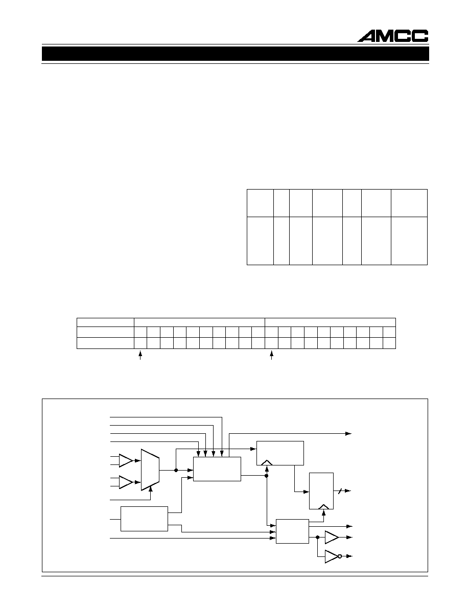
S2042 TRANSMITTER FUNCTIONAL
DESCRIPTION
The S2042 transmitter accepts parallel input data
and serializes it for transmission over fiber optic or
coaxial cable media. The chip is fully compatible with
the ANSI X3T11 Fibre Channel standard, and sup-
ports the Fibre Channel standard's data rates of 1062,
531 and 266 Mbit/sec.
The parallel input data word can be either 10 bits or
20 bits wide, depending upon DWS pin selection. A
block diagram showing the basic chip operation is
shown in Figure 3.
Figure 3. S2042 Functional Block Diagram
CONTROL
LOGIC
TEST
D(0..19)
OE1
OE0
DWS
REFCLK
REFSEL
RATESEL
2:1
10
10
20
10
DIVIDE-BY-2
PLL CLOCK
MULTIPLIER
F0 = F1 X 10/20
SHIFT
REGISTER
TX
TY
TLX
TLY
TCLK
TCLKN
DIVIDE-BY-2
D
Q
Parallel
Data In
S2042
Transmitter
S2043
Receiver
RefClk
Lock
Detect
RefClk
RCLK
Parallel
Data Out
Loopback
Loopback
Sync
Serial
Data
TCLK
Figure 2. Fibre Channel Interface Diagram
Applied Micro Circuits Corporation
6195 Lusk Blvd., San Diego, CA 92121 ∑ (619) 450-9333
3
HIGH PERFORMANCE SERIAL INTERFACE CIRCUITS
S2042/S2043
Reference Clock Input
The reference clock input (REFCLK) must be sup-
plied with a single-ended AC coupled crystal clock
source with 100 PPM tolerance to assure that the
transmitted data meets the Fibre Channel frequency
limits. The internal serial clock is frequency locked to
the reference clock. The word rate clock (TCLK, TCLKN)
output frequency is determined by the selected oper-
ating speed and word width. Refer to Table 1 for
TCLK/TCLKN clock frequencies.
Table 1. Transmitter Operating Modes
Data Rate
(Mbits/sec)
RATESEL
REFSEL
DWS
Word
Width
(Bits)
Reference
Clock
Frequency
(MHz)
1062.5
1062.5
531.25
531.25
265.625
0
0
1
1
Open
10
20
10
20
10
1
0
1
0
1
TCLK/TCLKN
Frequency
(MHz)
53.125
53.125
53.125
26.5625
26.5625
106.25
53.125
53.125
26.5625
26.5625
1
0
1
0
1
Parallel/Serial Conversion
The parallel-to-serial converter takes in 10-bit or 20-
bit wide data from the input latch and converts it to a
serial data stream. Parallel data is latched into the
transmitter on the positive going edge of REFCLK.
The data is then clocked synchronous to the clock
synthesis unit serial clock into the serial output shift
register. The shift register is clocked by the internally
generated bit clock which is 10 times the REFCLK
input frequency. The state of the serial outputs is
controlled by the output enable pins, OE0 and OE1.
D10 is transmitted first in 10-bit mode. D0 is trans-
mitted first in 20-bit mode. Table 2 shows the mapping
of the parallel data to the 8B/10B codes.
10-Bit/20-Bit Mode
The S2042 operates with either 10-bit or 20-bit par-
allel data inputs. Word width is selectable via the
DWS pin. In 10-bit mode, D10≠D19 are used and
D0≠D9 are ignored.
First Data Byte
Second Data Byte
19
18
17
16
15
14
13
12
11
10
j
h
g
f
i
e
d
c
b
a
9
8
7
6
5
4
3
2
1
0
TX[00:19] or
RX[00:19]
8b/10b alphabetic
representation
j
h
g
f
i
e
d
c
b
a
First bit transmitted in 20-bit mode
First bit transmitted in 10-bit mode
Table 2. Data Mapping to 8b/10b Alphabetic Representation
Figure 4. S2043 Functional Block Diagram
PLL CLOCK
RECOVERY
2:1
D
20
D
BITCLK
Q
SYNC
DETECT
LOGIC
CONTROL
LOGIC
RX
REFCLK
REFSEL
RATESEL
LOCK_REF
RY
RLX
RLY
LPEN
DWS
SYNCEN
LOCKDETN
D(0..19)
RCLK
SYNC
RCLKN
SHIFT
REGISTER
Applied Micro Circuits Corporation
6195 Lusk Blvd., San Diego, CA 92121 ∑ (619) 450-9333
4
HIGH PERFORMANCE SERIAL INTERFACE CIRCUITS
S2042/S2043
S2043 RECEIVER FUNCTIONAL
DESCRIPTION
The S2043 receiver is designed to implement the
ANSI X3T11 Fibre Channel specification receiver
functions. A block diagram showing the basic chip
function is provided in Figure 4.
Whenever a signal is present, the S2043 attempts to
achieve synchronization on both bit and transmis-
sion-word boundaries of the received encoded bit
stream. Received data from the incoming bit stream
is provided on the device's parallel data outputs.
The S2043 accepts serial encoded data from a fiber
optic or coaxial cable interface. The serial input stream
is the result of the serialization of 8B/10B encoded
data by an FC compatible transmitter. Clock recov-
ery is performed on-chip, with the output data
presented to the Fibre Channel transmission layer
as 10- or 20-bit parallel data. The chip is program-
mable to operate at the Fibre Channel specified
operating frequencies of 1062, 531 and 266 Mbit/s.
Serial/Parallel Conversion
Serial data is received on the RX, RY pins. The PLL
clock recovery circuit will lock to the data stream if the
clock to be recovered is within
±
100 PPM of the inter-
nally generated bit rate clock. The recovered clock is
used to retime the input data stream. The data is
then clocked into the serial to parallel output regis-
ters on the low going edge of RCLK. In 1062 Mbit/
sec, 10-bit mode, data is clocked out on the falling
edge of RCLK and RCLKN.The parallel data out can
be either 10 or 20 bits wide determined by the state
of the DWS pin. The word clock (RCLK) is synchro-
nized to the incoming data stream word boundary by
the detection of the fiber channel K28.5 synchroniza-
tion pattern (0011111010, positive running disparity).
10-Bit/20-Bit Mode
The S2043 will operate with either 10-bit or 20-bit
parallel data outputs. This option is selectable via
the DWS pin. See Table 4. In 10-bit mode, D10-D19
are used and D0-D9 are driven to the logic high state.
Reference Clock Input
The reference clock input must be supplied with a single-
ended AC coupled crystal clock source at
±
100 PPM
tolerance. See Table 4 for reference clock frequencies.
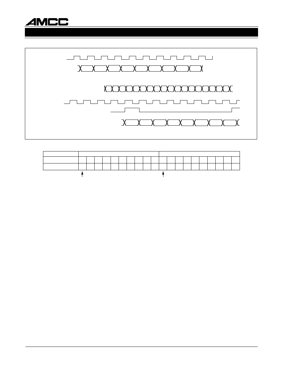
Framing
The S2043 provides SYNC character recognition and
data word alignment of the TTL level compatible output
data bus. In systems where the SYNC detect function
is undesired, a LOW on the SYNCEN input disables
the SYNC function and the data will be "un-framed".
First Data Byte
Second Data Byte
19
18
17
16
15
14
13
12
11
10
j
h
g
f
i
e
d
c
b
a
9
8
7
6
5
4
3
2
1
0
TX[00:19] or
RX[00:19]
8b/10b alphabetic
representation
j
h
g
f
i
e
d
c
b
a
First bit received in 20-bit mode
First bit received in 10-bit mode
Table 3. Data Mapping to 8b/10b Alphabetic Representation
REFCLK
(Input)
RCLK
(Output)
SYNC
(Output)
PARALLEL
DATA BUS
(Input)
K28.5,
Byte 1
of Data
Byte 2, 3
of Data
Byte 4, 5
of Data
Byte 6, 7
of Data
Byte 8, 9
of Data
Byte 10,
11 of Data
Byte 12,
13 of Data
Byte 14,15
of Data
K28.5
Byte 16
of Data
D1
D2
D3
D4
D5
D6
D7
D8
D9
D10
D11
D12
D13
D14
D15
PARALLEL
DATA BUS
(Output)
SERIAL DATA
S
2
0
4
2
S
2
0
4
3
K28.5
K28.5,
Byte 1
of Data
Byte 2, 3
of Data
Byte 4, 5
of Data
Byte 6, 7
of Data
Byte 8, 9
of Data
Byte 10,
11 of Data
Byte 12,
13 of Data
Byte 14,15
of Data
K28.5 D16
Figure 5. Functional Waveform
Applied Micro Circuits Corporation
6195 Lusk Blvd., San Diego, CA 92121 ∑ (619) 450-9333
5
HIGH PERFORMANCE SERIAL INTERFACE CIRCUITS
S2042/S2043
When framing is disabled by low SYNCEN, the S2043
simply achieves bit synchronization within 250 bit times
and begins to deliver parallel output data words whenever
it has received full transmission words. No attempt is made
to synchronize on any particular incoming character. The
SYNCEN input should be static during operation (i.e.
connected to VCC or GND). The S2043 will not main-
tain the existing byte synchronization when SYNCEN
transitions from the active to inactive state.
The SYNC output signal will go high whenever a
K28.5 character (positive disparity) is present on the
parallel data outputs. The SYNC output signal will be
low at all other times. This is true whether the S2043
is operating in 10-bit mode or in 20-bit mode. In 20-
bit mode, the K28.5 byte will always be placed in the
MSB (D0-D9). In 10-bit mode, the K28.5 will be
clocked with the RCLKN output.
Lock Detect
The S2043 lock detect function indicates the state of
the phase-locked loop (PLL) clock recovery unit. The
PLL will indicate lock within 250 bit times after the
start of receiving serial data inputs. If the serial data
inputs have an instantaneous phase jump (from a
serial switch, for example) the PLL will not indicate
an out-of-lock state, but will recover the correct phase
alignment within 250 bit times. If a run length of 64
bits is exceeded, or if the transition density is less
than 12%, the loop will be declared out of lock and
will attempt to re-acquire bit synchronization. When
lock is lost, the PLL will shift from the serial input
data to the reference clock, so that correct frequency
downstream clocking will be maintained.
In any transfer of PLL control from the serial data to
the reference clock, the RCLK/RCLKN output remains
phase continuous and glitch free, assuring the integ-
rity of downstream clocking.
Table 4. Receiver Operating Modes
Data Rate
(Mbits/sec)
RATESEL
REFSEL
DWS
Word
Width
(Bits)
Reference
Clock
Frequency
(MHz)
1062.5
1062.5
531.25
531.25
265.625
0
0
1
1
Open
10
20
10
20
10
1
0
1
0
1
RCLK/RCLKN
Frequency
(MHz)
53.125
53.125
53.125
26.5625
26.5625
106.25
53.125
53.125
26.5625
26.5625
1
0
1
0
1
Start-Up Procedure
The clock recovery PLL requires an initilization proce-
dure to correctly achieve lock on the serial data inputs.
At power-up or loss of lock, the PLL must first acquire
frequency lock to the local reference clock. This can be
accomplished in three ways: 1) The ≠LOCK_REF pin
can be connected to a 10 ms reset signal to initialize
the PLL. 2) By guaranteeing that no data is seen at the
serial data inputs for a minimum of 10 ms upon power-
up. 3) The S2043 can be put into the loopback mode
and the loopback outputs of the S2042 must be quies-
cent for a minimum of 10 ms after power-up.
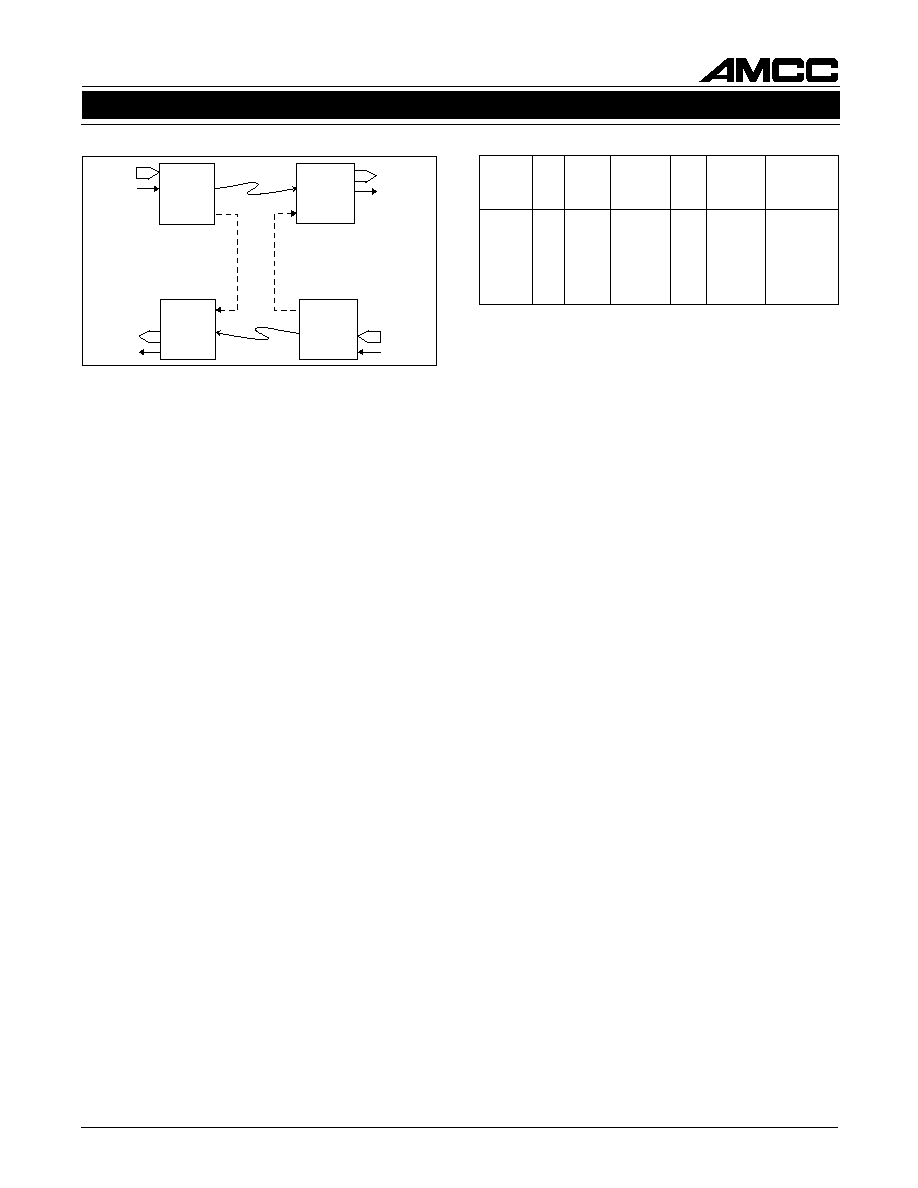
Other Operating Modes
Loopback
Local loopback requires a S2042 and a S2043 as shown
in the Figure 6. When enabled, serial data from the
S2042 transmitter is sent to the S2043 receiver, where
the clock is extracted and the data is deserialized. The
parallel data is then sent to the subsystem for verifica-
tion. This loopback mode provides the capability to
perform offline testing of the interface to guarantee the
integrity of the serial channel before enabling the trans-
mission medium. It also allows system diagnostics.
Operating Frequency Range
The S2042 and S2043 are optimized for operation at
the Fibre Channel rates of 266, 531 and 1062 Mbit/s.
Operation at other than Fibre channel rates is pos-
sible if the rate falls within
±
10% of the nominal rate.
REFCLK must be selected to be within 100 ppm of
the desired byte or word clock rate.
Test Modes
The TEST pin on the S2042 and the SYNCEN pin on
the S2043 provide a PLL bypass mode that can be
used for operating the digital area of the chip. In this
mode, clock signals are input through the reference
clock pins. This can be used for testing the device
during the manufacturing process or during an off-
line self-test. Sync detection is always enabled in
test mode.
Figure 6. Loopback Interface Diagram
Data In
S2042
Fibre
Channel
Transmitter
S2043
Fibre
Channel
Receiver
CLK
Data Out
Local
Loopback
S2043
Fibre
Channel
Receiver
S2042
Fibre
Channel
Transmitter
Local
Loopback
OE0, OE1
CLK
Data Out
Data In
OE0, OE1