 | –≠–ª–µ–∫—Ç—Ä–æ–Ω–Ω—ã–π –∫–æ–º–ø–æ–Ω–µ–Ω—Ç: S2044 | –°–∫–∞—á–∞—Ç—å:  PDF PDF  ZIP ZIP |
1
GLM COMPLIANT SERIAL INTERFACE CIRCUITS
S2044/S2045
BiCMOS PECL CLOCK GENERATOR
FEATURES
∑ Complies with the electrical and link levels of
the Gigabaud Link Module (GLM) specification
∑ Functionally compliant with ANSI X3T11 Fibre
Channel physical and transmission protocol
standards
∑ S2044 transmitter incorporates phase-locked
loop (PLL) providing clock synthesis from low-
speed reference
∑ S2045 receiver PLL configured for clock and
data recovery
∑ 1062 Mb/s (GLM), 531 Mb/s (HGLM) and
266 Mb/s (QGLM) operation
∑ 10- or 20-bit parallel TTL compatible interface
∑ 1 watt typical power dissipation for chipset
∑ +3.3/+5V power supply
∑ Low-jitter serial PECL compatible interface
∑ Lock detect
∑ Local loopback
∑ Compact 52 PQFP package
∑ Fibre Channel framing performed by receiver
∑ Continuous downstream clocking from receiver
∑ TTL compatible outputs possible with +5V I/O
power supply
APPLICATIONS
High-speed data communications
∑ Mainframe/Workstation
∑ Switched networks
∑ Proprietary extended backplanes
∑ Mass storage devices/RAID drives
GENERAL DESCRIPTION
The S2044 and S2045 transmitter and receiver pair
are designed to perform high-speed serial data trans-
mission over fiber optic or coaxial cable interfaces
conforming to the requirements of the ANSI X3T11
Fibre Channel specification. The chipset is Gigabaud
Link Module (GLM) compliant and supports 1062 Mb/s
(GLM) and 531 Mb/s Half-GLM (HGLM) and 266 Mb/s
Quarter-GLM (QGLM) modes with associated 10 or
20-bit data word.
The chipset performs parallel-to-serial and serial-to-
parallel conversion and framing for block-encoded
data. The S2044 on-chip PLL synthesizes the high-
speed clock from a low-speed reference. The S2045
on-chip PLL synchronizes directly to incoming digital
signals, to receive the data stream. The transmitter
and receiver each support differential PECL-compat-
ible I/O for fiber optic component interfaces, to
minimize crosstalk and maximize data integrity. Local
loopback allows for system diagnostics. The I/O sec-
tion can operate from either a +3.3V or a +5V power
supply. With a 3.3V power supply the chipset dissi-
pates only 1W typically.
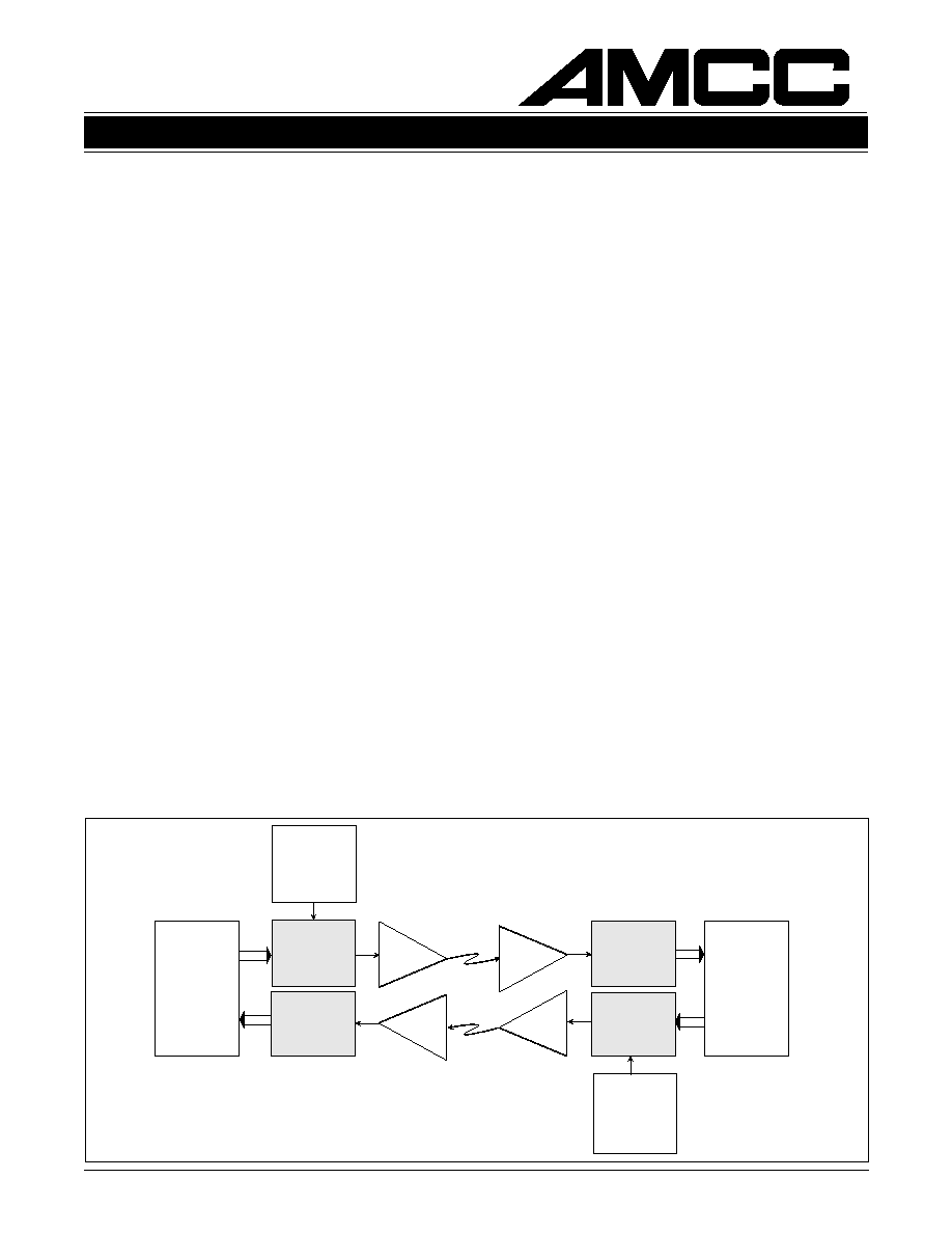
Figure 1 shows a typical network configuration incor-
porating the chipset. The chipset is compatible with
AMCC's S2036 Open Fiber Control (OFC) device.
Figure 1. System Block Diagram
Optical
TX
Optical
RX
Optical
RX
Optical
TX
S2045
RX
S2044
TX
S2036
Open
Fiber
Control
(OFC)
S2036
Open
Fiber
Control
(OFC)
S2044
TX
S2045
RX
Fibre
Channel
Controller
Fibre
Channel
Controller
Æ
PRELIMINARY
DEVICE SPECIFICATION
S2044/S2045
GLM COMPLIANT SERIAL INTERFACE CIRCUITS
2
GLM COMPLIANT SERIAL INTERFACE CIRCUITS
S2044/S2045
Table 1. Transmitter Operating Modes
Data Rate
(Mbits/sec)
RATESEL
REFSEL
DWS
Word
Width
(Bits)
Reference
Clock
Frequency
(MHz)
1062.5
1062.5
531.25
531.25
265.625
0
0
1
1
Open
10
20
10
20
10
1
0
1
0
1
TCLK/TCLKN
Frequency
(MHz)
53.125
53.125
53.125
26.5625
26.5625
106.25
53.125
53.125
26.5625
26.5625
1
0
1
0
1
Loopback
Local loopback is supported by the chipset, and pro-
vides a capability for performing offline testing of the
interface to ensure the integrity of the serial channel
before enabling the transmission medium. It also al-
lows for system diagnostics.
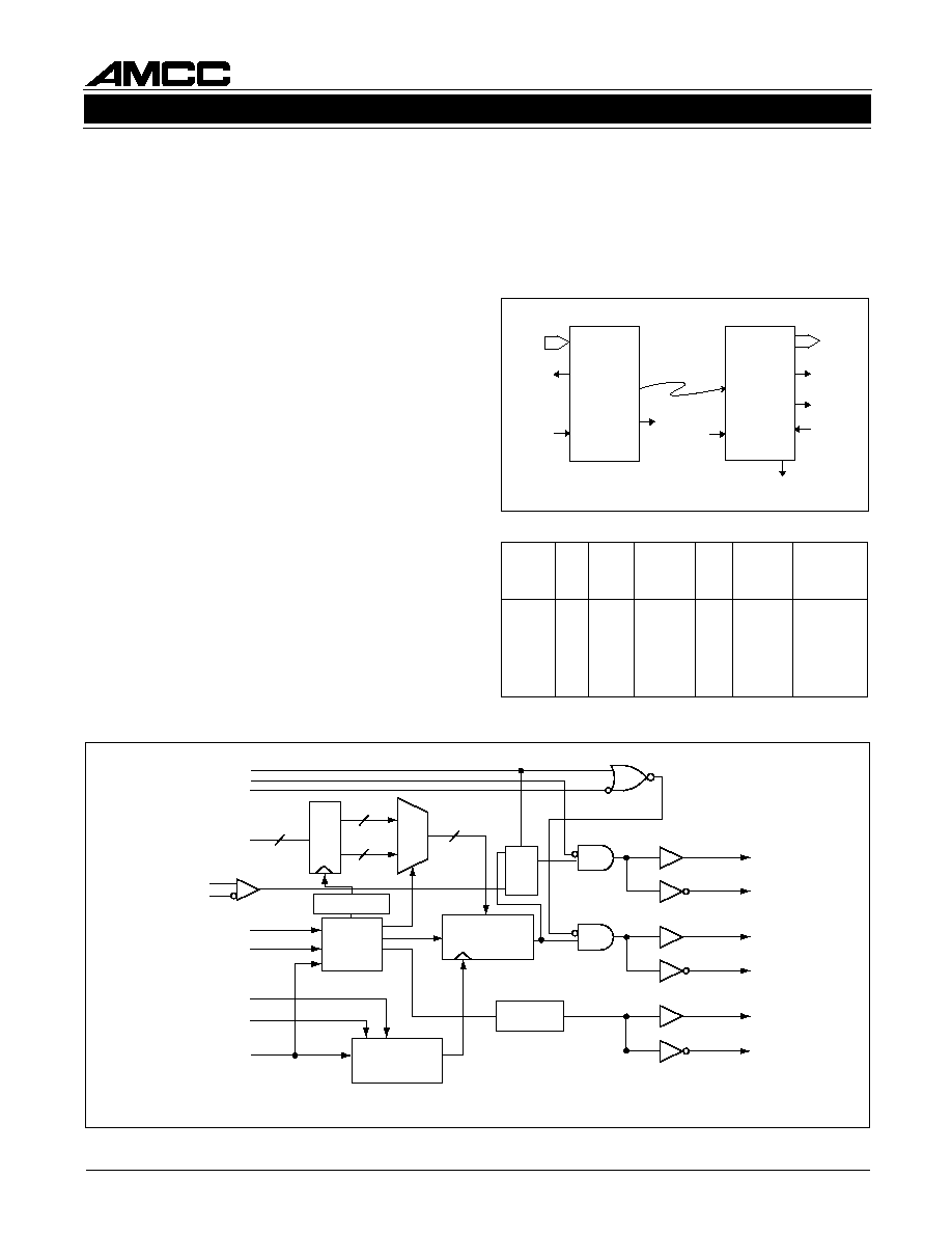
OVERVIEW
The S2044 transmitter and S2045 receiver provide
serialization and deserialization functions for block-
encoded data to implement a Fibre Channel interface.
Operation of the S2044/S2045 chips is straightfor-
ward, as depicted in Figure 2. The sequence of
operations is as follows:
Transmitter
1. 10/20-bit parallel input
2. Parallel-to-serial conversion
3. Serial output
Receiver
1. Clock and data recovery from serial input
2. Serial-to-parallel conversion
3. Frame detection
4. 10/20-bit parallel output
The 10/20-bit parallel data handled by the S2044 and
S2045 devices should be from a DC-balanced en-
coding scheme, such as the 8B/10B transmission
code, in which information to be transmitted is en-
coded 8 bits at a time into 10-bit transmission characters
1
.
Internal clocking and control functions are transparent to
the user. Details of data timing can be seen in Figure 5.
A lock detect feature is provided on the receiver, which
indicates that the PLL is locked (synchronized) to the
data stream.
1. A.X. Widmer and P.A. Franaszek, "A Byte-Oriented DC Balanced (0,4) 8B/10B Transmission Code," IBM Research Report RC 9391, May 1982.
Figure 2. Fibre Channel Interface Diagram
Parallel
Data In
S2044
Transmitter
S2045
Receiver
RefClk
Lock
Detect
RefClk
RCLK
Parallel
Data Out
Loopback
Loopback
Sync
Serial
Data
TCLK
CONTROL
LOGIC
TEST
[TX_SI]
[Tx(00:19)]
D(19..0)
OE1
[ ]
OE0
DWS
REFSEL
RATESEL
[+ SI]
[≠ SI]
[TBC]
REFCLK
2:1
10
10
20
10
DIVIDE-BY-2
PLL CLOCK
MULTIPLIER
F0 = F1 X 10/20
SHIFT
REGISTER
MUX
TX
TY
TLX
[+SO]
TLX
[-SO]
TCLK
TCLKN
DIVIDE-BY-2
D
0
1
Q
[ ]
= GLM Interface Pins
Figure 3. S2044 Functional Block Diagram

3
GLM COMPLIANT SERIAL INTERFACE CIRCUITS
S2044/S2045
First Data Byte
Second Data Byte
19
18
17
16
15
14
13
12
11
10
j
h
g
f
i
e
d
c
b
a
9
8
7
6
5
4
3
2
1
0
TX[00:19] or
RX[00:19]
8b/10b alphabetic
representation
j
h
g
f
i
e
d
c
b
a
First bit transmitted in 20-bit mode
First bit transmitted in 10-bit mode
Table 2. Data Mapping to 8b/10b Alphabetic Representation
Figure 4. S2045 Functional Block Diagram
PLL CLOCK
RECOVERY
2:1
D
20
D
BITCLK
Q
SYNC
DETECT
LOGIC
CONTROL
LOGIC
RX
RATESEL
REFSEL
[TBC]
REFCLK
[-LCK_REF]
LOCK_REF
RY
RLX
RLY
[EWRAP]
LPEN
DWS
[EN_CDET]
SYNCEN
LOCKDETN
[LUNUSE]
[FAULT]
[PARID1]
[STROBE ID]
D(0:19)
[RX(00:19)]
RCLK
[RBC1]
SYNC
[COM_DET]
RCLKN
[RBC0]
SHIFT
REGISTER
[ ]
GLM Interface PIns
S2044 TRANSMITTER FUNCTIONAL
DESCRIPTION
The S2044 transmitter accepts parallel input data
and serializes it for transmission over fiber optic or
coaxial cable media. The chip is fully compatible with
the ANSI X3T11 Fibre Channel standard, and sup-
ports the Fibre Channel standard's data rates of 1062,
531 and 266 Mbit/sec.
The parallel input data word can be either 10 bits or
20 bits wide, depending upon DWS pin selection. A
block diagram showing the basic chip function is
shown in Figure 3.
Parallel/Serial Conversion
The parallel-to-serial converter takes in 10-bit or 20-
bit wide data from the input latch and converts it to a
serial data stream. Parallel data is latched into the
transmitter on the positive going edge of REFCLK.
The data is then clocked synchronous to the clock
synthesis unit serial clock into the serial output shift
register. The shift register is clocked by the internally
generated bit clock which is 10 times the REFCLK
input frequency. The state of the serial outputs is
controlled by the output enable pins, OE0 and OE1.
D10 is transmitted first in 10-bit mode. D0 is transmit-
ted first in 20-bit mode. Table 2 shows the mapping
of the parallel data to the 8B/10B codes.
10-Bit/20-Bit Mode
The S2044 operates with either 10-bit or 20-bit parallel
data inputs. Word width is selectable via the DWS pin. In
10-bit mode, D10≠D19 are used and D0-D9 are ignored.
Reference Clock Input
The reference clock input (REFCLK) must be sup-
plied with a PECL single-ended AC coupled crystal
clock source with 100 PPM tolerance to assure that
the transmitted data meets the Fibre Channel fre-
quency limits. The internal serial clock is frequency
locked to the reference clock. The word rate clock
(TCLK, TCLKN) output frequency is determined by
the selected operating speed and word width. Refer
to Table 1 for TCLK/TCLKN clock frequencies.
4
GLM COMPLIANT SERIAL INTERFACE CIRCUITS
S2044/S2045
S2045 RECEIVER FUNCTIONAL
DESCRIPTION
The S2045 receiver is designed to implement the
ANSI X3T11 Fibre Channel specification receiver func-
tions. A block diagram showing the basic chip function
is provided in Figure 5.
Whenever a signal is present, the S2045 attempts to
achieve synchronization on both bit and transmission-
word boundaries of the received encoded bit stream.
Received data from the incoming bit stream is pro-
vided on the device's parallel data outputs.
The S2045 accepts serial encoded data from a fiber
optic or coaxial cable interface. The serial input stream
is the result of the serialization of 8B/10B encoded
data by an FC compatible transmitter. Clock recovery
is performed on-chip, with the output data presented
to the Fibre Channel transmission layer as 10- or 20-
bit parallel data. The chip is programmable to operate
at the Fibre Channel specified operating frequencies
of 1062, 531 and 266 Mbit/s.
Serial/Parallel Conversion
Serial data is received on the RX, RY pins. The PLL
clock recovery circuit will lock to the data stream if
the clock to be recovered is within
±
100 PPM of the
internally generated bit rate clock. The recovered clock
is used to retime the input data stream. The data is
then clocked into the serial to parallel output regis-
ters. The parallel data out can be either 10 or 20 bits
wide determined by the state of the DWS pin. The
word clock (RCLK) is synchronized to the incoming
data stream word boundary by the detection of the
fiber channel K28.5 synchronization pattern
(0011111010, positive running disparity).
10-Bit/20-Bit Mode
The S2045 will operate with either 10-bit or 20-bit
parallel data outputs. This option is selectable via the
DWS pin. See Tables 3 and 4. In 10-bit mode, D10≠
D19 are used and D0≠D9 are driven to the logic high state.
First Data Byte
Second Data Byte
19
18
17
16
15
14
13
12
11
10
j
h
g
f
i
e
d
c
b
a
9
8
7
6
5
4
3
2
1
0
TX[00:19] or
RX[00:19]
8b/10b alphabetic
representation
j
h
g
f
i
e
d
c
b
a
First bit received in 20-bit mode
First bit received in 10-bit mode
Table 3. Data Mapping to 8b/10b Alphabetic Representation
REFCLK
(Input)
RCLK
(Output)
SYNC
(Output)
PARALLEL
DATA BUS
(Input)
K28.5,
Byte 1
of Data
Byte 2, 3
of Data
Byte 4, 5
of Data
Byte 6, 7
of Data
Byte 8, 9
of Data
Byte 10,
11 of Data
Byte 12,
13 of Data
Byte 14,15
of Data
K28.5
Byte 16
of Data
D1
D2
D3
D4
D5
D6
D7
D8
D9
D10
D11
D12
D13
D14
D15
PARALLEL
DATA BUS
(Output)
SERIAL DATA
S
2
0
4
4
S
2
0
4
5
K28.5
K28.5,
Byte 1
of Data
Byte 2, 3
of Data
Byte 4, 5
of Data
Byte 6, 7
of Data
Byte 8, 9
of Data
Byte 10,
11 of Data
Byte 12,
13 of Data
Byte 14,15
of Data
K28.5 D16
Figure 5. Functional Waveform

5
GLM COMPLIANT SERIAL INTERFACE CIRCUITS
S2044/S2045
Figure 6. Loopback Diagram
Reference Clock Input
The reference clock input must be supplied with a
PECL single-ended AC coupled crystal clock source
at
±
100 PPM tolerance. See Table 4 for reference
clock frequencies.
Framing
The S2045 provides SYNC character recognition and
data word alignment of the TTL level compatible out-
put data bus. During the data realignment process,
the RCLK phase will be adjusted. No glitches will
occur in the RCLK signal due to the realignment. In
systems where the SYNC detect function is undes-
ired, a LOW on the SYNCEN input disables the SYNC
function and the data will be "un-framed".
When framing is disabled by low SYNCEN, the S2045
simply achieves bit synchronization within 250 bit times
and begins to deliver parallel output data words when-
ever it has received full transmission words. No
attempt is made to synchronize on any particular in-
coming character.
The SYNC output signal will go high whenever a K28.5
character (positive disparity) is present on the parallel
data outputs. The SYNC output signal will be low at
all other times. This is true whether the S2045 is
operating in 10-bit mode or in 20-bit mode.
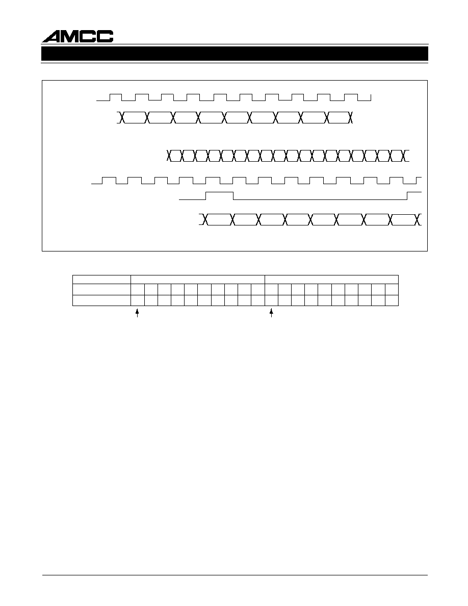
Lock Detect
The S2045 lock detect function indicates the state of
the phase-locked loop (PLL) clock recovery unit. The
PLL will indicate lock within 250 bit times after the
start of receiving serial data inputs. If the serial data
inputs have an instantaneous phase jump (from a
Data In
S2044
Fibre
Channel
Transmitter
S2045
Fibre
Channel
Receiver
CLK
Data Out
Local
Loopback
S2045
Fibre
Channel
Receiver
S2044
Fibre
Channel
Transmitter
Local
Loopback
OE0, OE1
CLK
Data Out
Data In
OE0, OE1
Data Rate
(Mbits/sec)
RATESEL
REFSEL
DWS
Word
Width
(Bits)
Reference
Clock
Frequency
(MHz)
1062.5
1062.5
531.25
531.25
265.625
0
0
1
1
Open
10
20
10
20
10
1
0
1
0
1
RCLK/RCLKN
Frequency
(MHz)
53.125
53.125
53.125
26.5625
26.5625
106.25
53.125
53.125
26.5625
26.5625
1
0
1
0
1
Table 4. Receiver Operating Modes
serial switch, for example) the PLL will not indicate
an out-of-lock state, but will recover the correct phase
alignment within 250 bit times. If a run length of 64
bits is exceeded, or if the transition density is less
than 12%, the loop will be declared out of lock and
will attempt to re-acquire bit synchronization. When
lock is lost, the PLL will shift from the serial input data
to the reference clock, so that correct frequency down-
stream clocking will be maintained.
In any transfer of PLL control from the serial data to
the reference clock, the RCLK/RCLKN output remains
phase continuous and glitch free, assuring the integ-
rity of downstream clocking.
Start-Up Procedure
The clock recovery PLL requires an initilization pro-
cedure to correctly achieve lock on the serial data
inputs. At power-up or loss of lock, the PLL must first
acquire frequency lock to the local reference clock.
This can be accomplished connecting the ≠LOCK_REF
pin to a 10 ms reset signal. If this is not possible, the
PLL can also be initialized by guaranteeing that no
data is seen at the serial data inputs for a minimum
of 10 ms upon power-up. If the serial data inputs
cannot be controlled, then the S2045 can be put into
the loopback mode and the loopback outputs of the
S2044 must be quiescent for a minimum of 10 ms
after power-up.