1
GIGABIT ETHERNET CHIPSET
S2046/S2050
March 29, 2000 / Revision B
BiCMOS PECL CLOCK GENERATOR
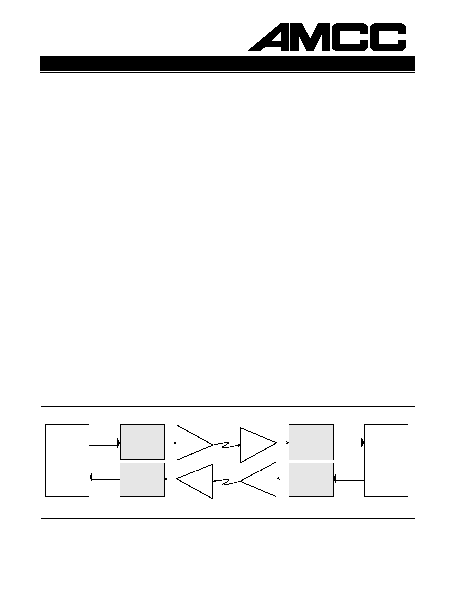
Figure 1. System Block Diagram
Æ
DEVICE
SPECIFICATION
S2046/S2050
GIGABIT ETHERNET CHIPSET
Optical
TX
Optical
RX
Optical
RX
Optical
TX
S2050
RX
S2046
TX
S2046
TX
S2050
RX
Gigabit
Ethernet
Controller
Gigabit
Ethernet
Controller
FEATURES
∑ Functionally compliant with the 802.3z specification
∑ S2046 transmitter incorporates phase-locked
loop (PLL) providing clock synthesis from low-
speed reference
∑ S2050 receiver PLL configured for clock and
data recovery
∑ 1250 Mbps (Gigabit Ethernet) operation
∑ 10- or 20-bit parallel TTL compatible interface
∑ +3.3/+5V power supply
∑ Low-jitter serial PECL compatible interface
∑ Lock detect
∑ Local loopback
∑ Compact 52 PQFP package
∑ Gigabit Ethernet framing performed by receiver
∑ Continuous downstream clocking from receiver
∑ TTL compatible outputs possible with +5V I/O
power supply
APPLICATIONS
High-speed data communications
∑ Ethernet backbone connections
∑ Mainframe
∑ Workstation
∑ Frame buffer
∑ Switched networks
∑ Data broadcast environments
∑ Proprietary extended backplanes
GENERAL DESCRIPTION
The S2046 and S2050 transmitter and receiver pair
are designed to perform high-speed serial data trans-
mission over fiber optic or coaxial cable interfaces
conforming to the requirements of the proposed 802.3z
specification. The chipset is Gigabit Ethernet compli-
ant and supports 1250 Mbps with an associated 10
or 20-bit data word.
The chipset performs parallel-to-serial and serial-to-
parallel conversion and framing for block-encoded
data. The S2046 on-chip PLL synthesizes the high-
speed clock from a low-speed reference. The S2050
on-chip PLL synchronizes directly to incoming digital
signals, to receive the data stream. The transmitter
and receiver each support differential PECL-compat-
ible I/O for fiber optic component interfaces, to
minimize crosstalk and maximize data integrity. Local
loopback allows for system diagnostics. The I/O sec-
tion can operate from either a +3.3V or a +5V power
supply. (See
Ordering Information.)
Figure 1 shows a typical network configuration incor-
porating the chipset.

2
GIGABIT ETHERNET CHIPSET
S2046/S2050
March 29, 2000 / Revision B
Figure 2. Interface Diagram
Parallel
Data In
S2046
Transmitter
S2050
Receiver
REFCLK
LOCKDETN
REFCLK
RCLK
Parallel
Data Out
RCLKN
Loopback
Loopback
SYNC
Serial
Data
TCLK
TCLKN
TLX/Y
TX/Y
RX/Y
RLX/Y
CONTROL
LOGIC
TEST
D[19:0]
OE1
OE0
DWS
REFSEL
REFCLK
2:1
10
10
20
10
PLL CLOCK
MULTIPLIER
F0 = F1 X 10/20
SHIFT
REGISTER
TX
TY
TLX
TLY
TCLK
TCLKN
DIVIDE-BY-2
D
Q
Figure 3. S2046 Functional Block Diagram
S2046/S2050 OVERVIEW
The S2046 transmitter and S2050 receiver provide
serialization and deserialization functions for block-
encoded data to implement a Gigabit interface.
Operation of the S2046/S2050 chips is straightfor-
ward, as depicted in Figure 2. The sequence of
operations is as follows:
Transmitter
1. 10/20-bit parallel input
2. Parallel-to-serial conversion
3. Serial output
Receiver
1. Clock and data recovery from serial input
2. Serial-to-parallel conversion
3. Frame detection
4. 10/20-bit parallel output
The 10/20-bit parallel data handled by the S2046 and
S2050 devices should be from a DC-balanced en-
coding scheme, such as the 8B/10B transmission
code, in which information to be transmitted is en-
coded 8 bits at a time into 10-bit transmission
characters.
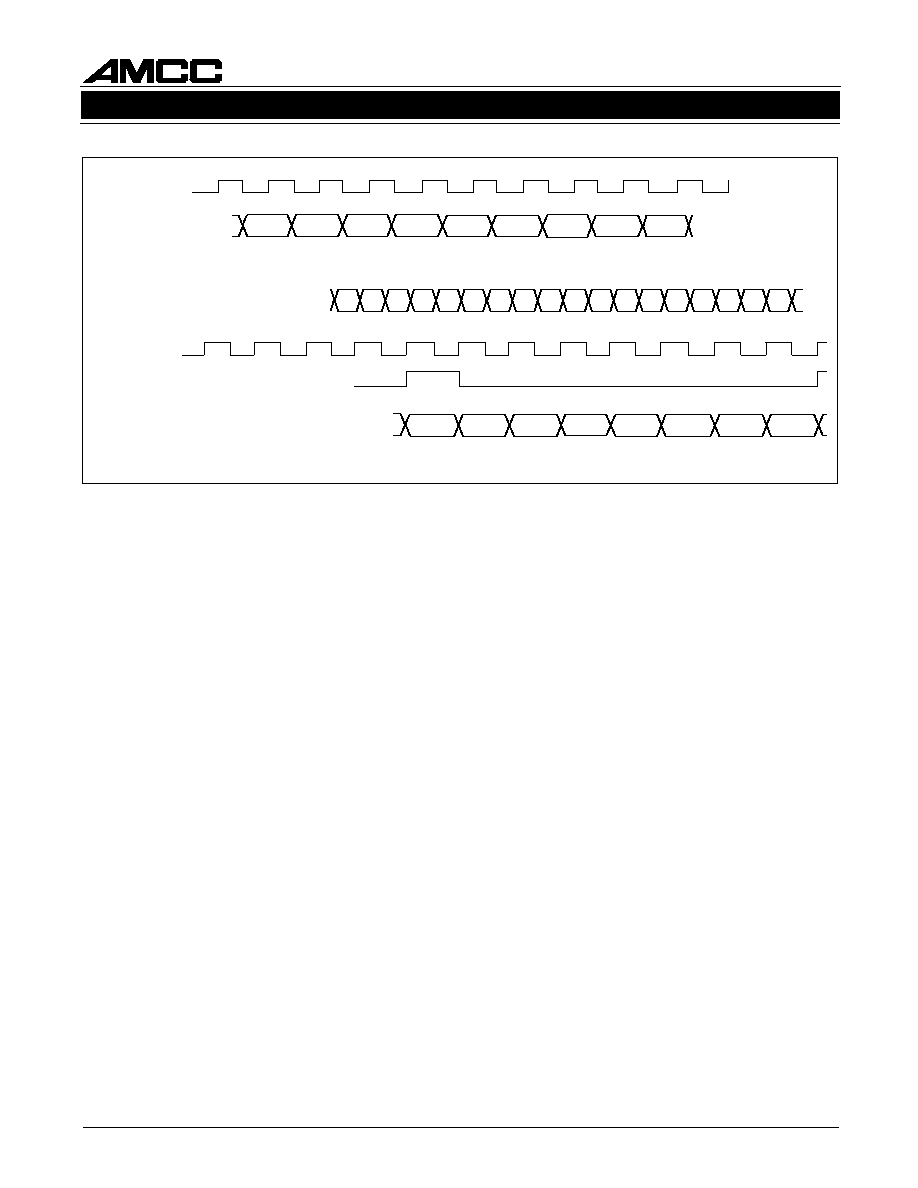
Internal clocking and control functions are transpar-
ent to the user. Details of data timing can be seen in
Figure 5.
A lock detect feature is provided on the receiver,
which indicates that the PLL is locked (synchronized)
to the data stream.
Loopback
Local loopback is supported by the chipset, and pro-
vides a capability for performing offline testing of the
interface to ensure the integrity of the serial channel
before enabling the transmission medium. It also al-
lows for system diagnostics.
S2046 TRANSMITTER
Architecture/Functional Description
The S2046 transmitter accepts parallel input data and
serializes it for transmission over fiber optic or coaxial
cable media. The S2046 is fully compliant with the
proposed 802.3z Specification, and supports the Gi-
gabit Ethernet data rate of 1250 Mbps.

3
GIGABIT ETHERNET CHIPSET
S2046/S2050
March 29, 2000 / Revision B
Table 1. Transmitter Operating Modes
Data Rate
(Mbps/sec)
REFSEL
DWS
Word
Width
(Bits)
Reference
Clock
Frequency
(MHz)
1250.0
1250.0
20
10
0
1
TCLK/TCLKN
Frequency
(MHz)
62.5
62.5
62.5
125.0
0
1
Table 2. Data Mapping to 8B/10B Alphabetic Representation
Figure 4. S2050 Functional Block Diagram
PLL CLOCK
RECOVERY
2:1
D
20
D
BITCLK
Q
SYNC
DETECT
LOGIC
CONTROL
LOGIC
RX
REFSEL
REFCLK
LOCKREFN
RY
RLX
RLY
LPEN
DWS
SYNCEN
LOCKDETN
D(0:19)
RCLK
SYNC
RCLKN
SHIFT
REGISTER
DIVIDER
The parallel input data word can be either 10 bits or
20 bits wide, depending upon DWS pin selection. A
block diagram showing the basic chip function is
shown in Figure 3.
Parallel/Serial Conversion
The parallel-to-serial converter takes in 10-bit or 20-
bit wide data from the input latch and converts it to a
serial data stream. Parallel data is latched into the
transmitter on the positive going edge of REFCLK.
The data is then clocked synchronous to the clock
synthesis unit serial clock into the serial output shift
register. The shift register is clocked by the internally
generated bit clock which is 10 or 20 times the
REFCLK input frequency. The state of the serial out-
puts is controlled by the output enable pins, OE0 and
OE1. D[10] is transmitted first in 10-bit mode. D[0] is
transmitted first in 20-bit mode. Table 2 shows the
mapping of the parallel data to the 8B/10B codes.
10-Bit/20-Bit Mode
The S2046 operates with either 10-bit or 20-bit paral-
lel data inputs. Word width is selectable via the DWS
pin. In 10-bit mode, D[10-19] are used and D[0-9] are
ignored. See Table 2.
Reference Clock Input
The reference clock input (REFCLK) must be supplied
with a PECL single-ended AC coupled crystal clock
source with 100 PPM tolerance to assure that the trans-
mitted data meets the proposed 802.3z Specification
frequency limits. The internal serial clock is frequency
locked to the reference clock. Refer to Table 1 for
reference clock frequencies.
e
t
y
B
a
t
a
D
t
s
r
i
F
e
t
y
B
a
t
a
D
d
n
o
c
e
S
r
o
]
9
1
:
0
[
X
T
]
9
1
:
0
[
X
R
0
1
2
3
4
5
6
7
8
9
0
1
1
1
2
1
3
1
4
1
5
1
6
1
7
1
8
1
9
1
c
i
t
e
b
a
h
p
l
a
B
0
1
/
B
8
n
o
i
t
a
t
n
e
s
e
r
p
e
r
a
b
c
d
e
f
g
h
i
j
a
b
c
d
e
f
g
h
i
j
First bit transmitted in 10-bit mode
First bit transmitted in 20-bit mode
4
GIGABIT ETHERNET CHIPSET
S2046/S2050
March 29, 2000 / Revision B
1. A.X. Widmer and P.A. Franaszek, "A Byte-Oriented DC Balanced (0,4) 8B/10B Transmission Code," IBM Research Report RC 9391,
May 1982.
REFCLK
(Input)
RCLK
(Output)
SYNC
(Output)
PARALLEL
DATA BUS
(Input)
K28.5,
Byte 1
of Data
Byte 2, 3
of Data
Byte 4, 5
of Data
Byte 6, 7
of Data
Byte 8, 9
of Data
Byte 10,
11 of Data
Byte 12,
13 of Data
Byte 14,15
of Data
K28.5
Byte 16
of Data
D1
D2
D3
D4
D5
D6
D7
D8
D9
D10
D11
D12
D13
D14
D15
PARALLEL
DATA BUS
(Output)
SERIAL DATA
S
2
0
4
6
S
2
0
5
0
K28.5
K28.5,
Byte 1
of Data
Byte 2, 3
of Data
Byte 4, 5
of Data
Byte 6, 7
of Data
Byte 8, 9
of Data
Byte 10,
11 of Data
Byte 12,
13 of Data
Byte 14,15
of Data
K28.5 D16
Figure 5. Functional Waveform
S2050 RECEIVER
Architecture/Functional Description
The S2050 receiver is designed to implement the
802.3z specification receiver functions. A block dia-
gram showing the basic chip function is provided in
Figure 4.
Whenever a signal is present, the S2050 attempts to
achieve synchronization on both bit and transmission-
word boundaries of the received encoded bit stream.
Received data from the incoming bit stream is pro-
vided on the device's parallel data outputs.
The S2050 accepts serial encoded data from a fiber
optic or coaxial cable interface. The serial input stream
is the result of the serialization of 8B/10B encoded
data by a compatible transmitter. Clock recovery is
performed on-chip, with the output data presented to
the transmission layer as 10- or 20-bit parallel data.
The chip operates at the Gigabit Ethernet frequency
of 1250 Mbps.
Serial/Parallel Conversion
Serial data is received on the RX, RY pins. The PLL
clock recovery circuit will lock to the data stream if
the clock to be recovered is within
±
100 PPM of the
internally generated bit rate clock. The recovered clock
is used to retime the input data stream. The data is
then clocked into the serial to parallel output regis-
ters. The parallel data out can be either 10 or 20 bits
wide determined by the state of the DWS pin. The
word clock (RCLKN) is synchronized to the incoming
data stream word boundary by the detection of the
COMMA synchronization pattern (0011111XXX, positive
running disparity).
10-Bit/20-Bit Mode
The S2050 will operate with either 10-bit or 20-bit par-
allel data outputs. This option is selectable via the
DWS pin. See Tables 2 and 3. In 10-bit mode, the
10:bit data word is output on D[10:19], and D[0:9] are
driven to the logic high state.

5
GIGABIT ETHERNET CHIPSET
S2046/S2050
March 29, 2000 / Revision B
Figure 6. Interface Diagram
Data In
S2046
Gigabit
Ethernet
Transmitter
S2050
Gigabit
Ethernet
Receiver
RCLK
Data Out
Local
Loopback
S2050
Gigabit
Ethernet
Receiver
S2046
Gigabit
Ethernet
Transmitter
Local
Loopback
TX/Y
TLX/Y
RX/Y
RLX/Y
TLX/Y
RX/Y
TX/Y
RLX/Y
OE1
OE0
LPEN
RCLK
Data Out
LPEN
Data In
OE0, OE1
Data Rate
(Mbits/sec)
REFSEL
DWS
Word
Width
(Bits)
Reference
Clock
Frequency
(MHz)
1250.0
1250.0
20
10
0
1
RCLK/RCLKN
Frequency
(MHz)
62.50
62.5
62.50
125.0
0
1
Table 3. Receiver Operating Modes
Table 4. Response of PLL Loop Circuit to Input Data Rate Variation
e
t
a
t
S
t
n
e
s
e
r
P
L
L
P
e
t
a
R
a
t
a
D
t
u
p
n
I
d
e
r
a
p
m
o
c
(
n
o
i
t
a
i
r
a
V
)
K
L
C
F
E
R
o
t
N
T
E
D
K
C
O
L
L
L
P
e
t
a
t
S
w
e
N
o
t
d
e
k
c
o
L
K
L
C
F
E
R
m
p
p
4
4
2
-
0
L
>
-
-
H
a
t
a
d
t
u
p
n
i
o
t
d
e
k
c
o
L
m
p
p
6
6
3
-
4
4
2
e
t
a
n
i
m
r
e
t
e
d
n
I
e
t
a
n
i
m
r
e
t
e
d
n
I
m
p
p
6
6
3
>
H
K
L
C
_
F
E
R
o
t
d
e
k
c
o
L
o
t
d
e
k
c
o
L
a
t
a
D
t
u
p
n
I
m
p
p
8
4
4
-
0
L
a
t
a
D
t
u
p
n
I
o
t
d
e
k
c
o
L
m
p
p
2
3
7
-
8
4
4
e
t
a
n
i
m
r
e
t
e
d
n
I
e
t
a
n
i
m
r
e
t
e
d
n
I
m
p
p
2
3
7
>
H
>
-
-
L
K
L
C
_
F
E
R
o
t
d
e
k
c
o
L
Reference Clock Input
The reference clock input must be supplied with a PECL
single-ended AC coupled crystal clock source at
±
100 PPM
tolerance. See Table 3 for reference clock frequencies.
Framing
The S2050 provides SYNC character recognition and
data word alignment of the TTL level compatible out-
put data bus. During the data realignment process,
the RCLKN phase will be adjusted, and the byte pre-
vious to the comma character will be lost. No glitches
will occur in the RCLKN signal due to the realign-
ment. In systems where the SYNC detect function is
undesired, a LOW on the SYNCEN input disables the
SYNC function and the data will be "unframed".
When framing is disabled by low SYNCEN, the S2050
simply achieves bit synchronization and begins to de-
liver parallel output data words whenever it has
received full transmission words. No attempt is made
to synchronize on any particular incoming character.
The SYNC output signal will go high whenever a
COMMA character (0011111XXX, positive running dis-
parity) is present on the parallel data outputs. The
SYNC output signal will be low at all other times. This
is true whether the S2050 is operating in 10-bit mode
or in 20-bit mode.
Lock Detect
The S2050 lock detect function indicates the state of
the phase-locked loop (PLL) clock recovery unit. The
PLL will indicate lock within 2.5
µ
s after the start of
receiving serial data inputs. If the serial data inputs
have an instantaneous phase jump (from a serial
switch, for example) the PLL will not indicate an out-
of-lock state, but will recover the correct phase
alignment. If a run length of 80-160 bits is exceeded
the loop will declare loss of lock. Input data rate varia-
tion (compared to REFCLK) can also cause loss of
lock. Table 4 shows the response of the PLL loop
circuit to input data rate variation. When lock is lost,
the PLL will attempt to reacquire bit synchronization,
and will shift from the serial input data to the refer-
ence clock so that the correct frequency downstream
clocking will be maintained.

6
GIGABIT ETHERNET CHIPSET
S2046/S2050
March 29, 2000 / Revision B
The LOCKDETN output will go to inactive when no
data is present on the serial data inputs. When
LOCKDETN is in the inactive state, it indicates that
the PLL is locking to the local reference clock to main-
tain downstream clocking. When LOCKDETN is in
the active state, it indicates that the PLL is attempting
to lock to the incoming serial data. When serial data
is restored, the LOCKDETN output will stay in the
active state.
When lock is lost, the PLL will attempt to reacquire bit
synchronization, and will shift from the serial input
data to the reference clock so that the correct down-
stream clocking will be maintained. The PLL will
continuously shift between the reference clock and
the input data until input data has been restored. While
the PLL is locked to the reference clock, LOCKDETN
will remain active, with one exception: when all of the
following conditions are met, the LOCKDETN output
toggle between active and inactive, reflecting the in-
ternal PLL shift between reference clock and input
data: (a) LOCKREFN is not active; (b) the signal (or
noise) on the high-speed input is above the voltage
input sensitivity threshold; (c) the signal (or noise) on
the high-speed input varies from the reference clock
by more than 244 ppm, and (d) the signal (or noise)
on the high-speed input passes the run length crite-
ria. When these conditions are met, LOCKDETN will
toggle, and the RCLK/RCLKN outputs will also shift
slightly in frequency.
In any transfer of PLL control from the serial data to
the reference clock, the RCLK/RCLKN output remains
phase continuous and glitch free, assuring the integ-
rity of downstream clocking.
OTHER OPERATING MODES
Loopback
The S2046 and S2050 have secondary high-speed I/O
to provide a local loopback path. The local loopback
configuration is shown in Figure 6. When OE1 is ac-
tive on the S2046, the high-speed data is passed out
the TLX/Y output. Operation of the TLX/Y output is
independent of the TX/Y output--data can be simul-
taneously output on both. With LPEN active on the
S2050, data on the RLX/Y input is passed through to
the parallel output. The local loopback path provides
the capability to perform off-line testing and system
diagnostics.
Operating Frequency Range
The S2046 and S2050 are optimized for operation at
the Gigabit Ethernet rate of 1250.0 Mbit/s. REFCLK
must be selected to be within 100 ppm of the desired
byte or word clock rate.
Test Modes
The TEST pin on the S2046 and the SYNCEN pin on
the S2050 provide a PLL bypass mode that can be
used for operating the digital area of the chip. In this
mode, clock signals are input through the reference
clock pins. This can be used for testing the device
during the manufacturing process or during an off-line
self-test. Sync detection is always enabled in test mode.
The SYNCEN input on the S2050 must transition
through mid-state in less than five REFCLK periods
to insure that PLL bypass mode is not exerted. In
order to guarantee that the S2050 enters PLL bypass
mode, SYNCEN must be held in mid state for more
than seven REFCLK cycles.

7
GIGABIT ETHERNET CHIPSET
S2046/S2050
March 29, 2000 / Revision B
Table 5. S2046 Pin Assignment and Descriptions
e
m
a
N
n
i
P
l
e
v
e
L
O
/
I
#
n
i
P
n
o
i
t
p
i
r
c
s
e
D
9
1
D
8
1
D
7
1
D
6
1
D
5
1
D
4
1
D
3
1
D
2
1
D
1
1
D
0
1
D
9
D
8
D
7
D
6
D
5
D
4
D
3
D
2
D
1
D
0
D
L
T
T
I
0
5
9
4
8
4
7
4
4
4
3
4
2
4
1
4
8
3
7
3
6
3
5
3
1
3
0
3
9
2
8
2
5
2
4
2
3
2
2
2
f
o
e
g
d
e
g
n
i
s
i
r
e
h
t
n
o
n
i
d
e
k
c
o
l
c
s
i
a
t
a
D
.
a
t
a
D
t
u
p
n
I
l
e
ll
a
r
a
P
t
i
b
-
0
1
n
I
.
t
s
r
i
f
d
e
t
t
i
m
s
n
a
r
t
s
i
]
0
[
D
,
e
d
o
m
t
i
b
-
0
2
n
I
.
K
L
C
F
E
R
s
i
]
0
1
[
D
d
n
a
,
d
e
r
o
n
g
i
e
r
a
]
9
:
0
[
D
,
d
e
s
u
e
r
a
]
9
1
:
0
1
[
D
,
e
d
o
m
.
t
s
r
i
f
d
e
t
t
i
m
s
n
a
r
t
D
N
G
D
N
G
--
0
2
.
d
n
u
o
r
g
o
t
d
e
t
c
e
n
n
o
c
e
b
t
s
u
m
n
i
p
s
i
h
T
S
W
D
c
i
t
a
t
S
L
T
T
I
9
1
a
t
a
d
l
e
ll
a
r
a
p
e
h
t
s
t
c
e
l
e
s
n
i
p
s
i
h
t
n
o
l
e
v
e
l
e
h
T
.
t
c
e
l
e
S
h
t
d
i
W
a
t
a
D
,
d
e
t
c
e
l
e
s
s
i
h
t
d
i
w
s
u
b
l
e
ll
a
r
a
p
t
i
b
-
0
2
a
,
W
O
L
n
e
h
W
.
h
t
d
i
w
s
u
b
s
i
s
u
b
a
t
a
d
l
e
ll
a
r
a
p
t
i
b
-
0
1
a
,
H
G
I
H
n
e
h
W
.
e
v
i
t
c
a
e
r
a
]
9
1
:
0
[
D
d
n
a
e
e
S
(
.
d
e
s
u
t
o
n
e
r
a
]
9
:
0
[
D
d
n
a
e
v
i
t
c
a
e
r
a
]
9
1
:
0
1
[
D
,
d
e
t
c
e
l
e
s
.
)
1
e
l
b
a
T
1
E
O
c
i
t
a
t
S
L
T
T
I
1
n
e
h
W
.
s
t
u
p
t
u
o
Y
L
T
/
X
L
T
r
o
f
l
o
r
t
n
o
c
e
l
b
a
n
E
t
u
p
t
u
O
W
O
L
e
v
i
t
c
A
.
e
t
a
t
s
w
o
l
c
i
g
o
l
e
h
t
n
i
n
i
a
m
e
r
d
n
a
d
e
l
b
a
s
i
d
e
r
a
Y
L
T
/
X
L
T
,
e
v
i
t
c
a
n
i
0
E
O
c
i
t
a
t
S
L
T
T
I
2
n
e
h
W
.
s
t
u
p
t
u
o
Y
T
/
X
T
r
o
f
l
o
r
t
n
o
c
e
l
b
a
n
E
t
u
p
t
u
O
W
O
L
e
v
i
t
c
A
.
e
t
a
t
s
w
o
l
c
i
g
o
l
e
h
t
n
i
n
i
a
m
e
r
d
n
a
d
e
l
b
a
s
i
d
e
r
a
Y
T
/
X
T
,
e
v
i
t
c
a
n
i
K
L
C
F
E
R
L
C
E
P
I
6
1
-
l
a
t
s
y
r
c
A
)
.
d
e
l
p
u
o
c
y
l
e
v
i
t
i
c
a
p
a
c
y
ll
a
n
r
e
t
x
E
(
.
k
c
o
l
C
e
c
n
e
r
e
f
e
R
e
h
T
.
r
e
il
p
i
t
l
u
m
k
c
o
l
c
L
L
P
e
h
t
r
o
f
k
c
o
l
c
e
c
n
e
r
e
f
e
r
d
e
ll
o
r
t
n
o
c
)
.
1
e
l
b
a
T
e
e
S
(
.
n
i
p
L
E
S
F
E
R
e
h
t
y
b
t
e
s
s
i
K
L
C
F
E
R
f
o
y
c
n
e
u
q
e
r
f
K
L
C
T
N
K
L
C
T
.
f
f
i
D
L
T
T
O
2
1
1
1
d
n
a
e
u
r
t
k
c
o
l
c
e
t
a
r
d
r
o
w
L
T
T
l
a
i
t
n
e
r
e
f
f
i
D
.
k
c
o
l
C
t
i
m
s
n
a
r
T
.
y
c
n
e
u
q
e
r
f
r
o
f
1
e
l
b
a
T
e
e
S
.
t
n
e
m
e
l
p
m
o
c
X
L
T
Y
L
T
.
f
f
i
D
L
C
E
P
O
5
4
t
a
h
t
s
t
u
p
t
u
o
L
C
E
P
l
a
i
t
n
e
r
e
f
f
i
D
.
t
u
p
t
u
O
k
c
a
b
p
o
o
L
l
a
i
r
e
S
t
i
m
s
n
a
r
T
o
t
d
e
d
n
e
t
n
i
e
r
a
y
e
h
T
.
Y
T
d
n
a
X
T
o
t
t
n
e
l
a
v
i
u
q
e
y
ll
a
n
o
i
t
c
n
u
f
e
r
a
e
h
t
s
i
X
L
T
.
1
E
O
y
b
d
e
l
b
a
n
E
.
g
n
i
t
s
e
t
k
c
a
b
p
o
o
l
r
o
f
d
e
s
u
e
b
.
t
u
p
t
u
o
e
v
i
t
a
g
e
n
e
h
t
s
i
Y
L
T
d
n
a
,
t
u
p
t
u
o
e
v
i
t
i
s
o
p
Y
T
X
T
.
f
f
i
D
L
C
E
P
O
9
8
t
i
m
s
n
a
r
t
t
a
h
t
s
t
u
p
t
u
o
L
C
E
P
l
a
i
t
n
e
r
e
f
f
i
D
.
t
u
p
t
u
O
l
a
i
r
e
S
t
i
m
s
n
a
r
T
0
5
1
e
v
i
r
d
d
n
a
a
t
a
d
l
a
i
r
e
s
e
h
t
.
d
n
u
o
r
g
o
t
X
T
.
0
E
O
y
b
d
e
l
b
a
n
E
.
t
u
p
t
u
o
e
v
i
t
a
g
e
n
e
h
t
s
i
Y
T
d
n
a
,
t
u
p
t
u
o
e
v
i
t
i
s
o
p
e
h
t
s
i

8
GIGABIT ETHERNET CHIPSET
S2046/S2050
March 29, 2000 / Revision B
e
m
a
N
n
i
P
l
e
v
e
L
O
/
I
#
n
i
P
n
o
i
t
p
i
r
c
s
e
D
L
E
S
F
E
R
c
i
t
a
t
S
L
T
T
I
8
1
e
e
S
(
.
y
c
n
e
u
q
e
r
f
k
c
o
l
c
e
c
n
e
r
e
f
e
r
e
h
t
s
t
c
e
l
e
S
.
t
c
e
l
e
S
e
c
n
e
r
e
f
e
R
)
.
1
e
l
b
a
T
C
C
V
L
C
E
V
3
.
3
+
≠
9
3
,
1
2
V
3
.
3
+
e
r
o
C
D
N
G
L
T
T
D
N
G
≠
,
5
1
,
4
1
4
3
d
n
u
o
r
G
L
T
T
C
C
V
L
T
T
/
V
5
+
V
3
.
3
≠
7
1
y
l
p
p
u
S
r
e
w
o
P
L
T
T
C
C
V
O
I
L
C
E
V
3
.
3
+
≠
0
1
,
3
y
l
p
p
u
S
r
e
w
o
P
O
/
I
L
C
E
P
E
E
V
O
I
L
C
E
D
N
G
≠
7
,
6
D
N
G
O
/
I
L
C
E
P
C
C
V
A
V
3
.
3
+
≠
2
3
,
7
2
y
l
p
p
u
S
r
e
w
o
P
g
o
l
a
n
A
E
E
V
A
D
N
G
≠
3
3
,
6
2
d
n
u
o
r
G
g
o
l
a
n
A
E
E
V
L
C
E
D
N
G
≠
,
0
4
,
3
1
2
5
,
1
5
d
n
u
o
r
G
e
r
o
C
C
N
≠
≠
6
4
,
5
4
d
e
t
c
e
n
n
o
C
t
o
N
Table 5. S2046 Pin Assignment and Descriptions (Continued)

9
GIGABIT ETHERNET CHIPSET
S2046/S2050
March 29, 2000 / Revision B
Table 6. S2050 Pin Assignment and Descriptions
e
m
a
N
n
i
P
l
e
v
e
L
O
/
I
#
n
i
P
n
o
i
t
p
i
r
c
s
e
D
9
1
D
8
1
D
7
1
D
6
1
D
5
1
D
4
1
D
3
1
D
2
1
D
1
1
D
0
1
D
9
D
8
D
7
D
6
D
5
D
4
D
3
D
2
D
1
D
0
D
L
T
T
O
5
4
3
4
2
4
0
4
8
3
7
3
5
3
4
3
2
3
1
3
9
2
8
2
5
2
4
2
2
2
1
2
8
1
7
1
5
1
4
1
s
i
s
u
b
a
t
a
d
l
e
ll
a
r
a
p
e
h
t
f
o
h
t
d
i
w
e
h
T
.
a
t
a
d
t
u
p
t
u
o
l
e
ll
a
r
a
P
s
i
s
u
b
s
i
h
t
n
o
a
t
a
d
l
e
ll
a
r
a
P
.
n
i
p
S
W
D
e
h
t
f
o
e
t
a
t
s
e
h
t
y
b
d
e
t
c
e
l
e
s
s
i
]
0
[
D
,
e
d
o
m
t
i
b
-
0
2
n
I
.
K
L
C
R
f
o
e
g
d
e
g
n
il
l
a
f
e
h
t
n
o
t
u
o
d
e
k
c
o
l
c
d
n
a
d
e
s
u
e
r
a
]
0
1
:
9
1
[
D
,
e
d
o
m
t
i
b
-
0
1
n
I
.
d
e
v
i
e
c
e
r
t
i
b
t
s
r
i
f
e
h
t
e
h
t
s
i
]
0
1
[
D
,
e
d
o
m
t
i
b
-
0
1
n
I
.
e
t
a
t
s
h
g
i
h
e
h
t
o
t
n
e
v
i
r
d
e
r
a
]
0
:
9
[
D
.
d
e
v
i
e
c
e
r
t
i
b
t
s
r
i
f
N
T
E
D
K
C
O
L
L
T
T
O
2
5
s
e
t
a
c
i
d
n
i
N
T
E
D
K
C
O
L
,
e
v
i
t
c
a
n
e
h
W
.
w
o
L
e
v
i
t
c
A
.
t
c
e
t
e
D
k
c
o
L
n
e
h
W
.
m
a
e
r
t
s
a
t
a
d
g
n
i
m
o
c
n
i
e
h
t
o
t
d
e
k
c
o
l
s
i
L
L
P
e
h
t
t
a
h
t
s
i
L
L
P
e
h
t
t
a
h
t
g
n
i
t
a
c
i
d
n
i
g
a
l
f
m
e
t
s
y
s
a
s
e
d
i
v
o
r
p
t
i
,
e
v
i
t
c
a
n
i
.
k
c
o
l
c
e
c
n
e
r
e
f
e
r
l
a
c
o
l
e
h
t
o
t
d
e
k
c
o
l
N
E
P
L
L
T
T
I
8
e
h
t
s
t
c
e
l
e
s
N
E
P
L
,
e
v
i
t
c
a
n
e
h
W
.
h
g
i
H
e
v
i
t
c
A
.
e
l
b
a
n
E
p
o
o
L
,
e
v
i
t
c
a
n
i
n
e
h
W
.
)
Y
L
R
,
X
L
R
(
s
n
i
p
t
u
p
n
i
l
a
i
r
e
s
l
a
i
t
n
e
r
e
f
f
i
d
k
c
a
b
p
o
o
l
.
)
n
o
i
t
a
r
e
p
o
l
a
m
r
o
n
(
Y
R
d
n
a
X
R
s
t
c
e
l
e
s
N
E
P
L
S
W
D
c
i
t
a
t
S
L
T
T
I
4
a
t
a
d
l
e
ll
a
r
a
p
e
h
t
s
t
c
e
l
e
s
n
i
p
s
i
h
t
n
o
l
e
v
e
l
e
h
T
.
t
c
e
l
e
S
h
t
d
i
W
a
t
a
D
,
d
e
t
c
e
l
e
s
s
i
h
t
d
i
w
s
u
b
l
e
ll
a
r
a
p
t
i
b
-
0
2
a
,
W
O
L
n
e
h
W
.
h
t
d
i
w
s
u
b
s
i
s
u
b
a
t
a
d
l
e
ll
a
r
a
p
t
i
b
-
0
1
a
,
H
G
I
H
n
e
h
W
.
e
v
i
t
c
a
e
r
a
]
0
:
9
1
[
D
d
n
a
e
e
S
(
.
H
G
I
H
o
g
ll
i
w
]
0
:
9
[
D
d
n
a
e
v
i
t
c
a
e
r
a
]
0
1
:
9
1
[
D
,
d
e
t
c
e
l
e
s
r
o
f
d
e
s
u
(
s
r
e
t
n
u
o
c
l
a
n
r
e
t
n
i
e
h
t
t
e
s
e
r
ll
i
w
e
g
d
e
g
n
i
s
i
r
A
)
.
3
e
l
b
a
T
.
)
t
s
e
t
K
L
C
R
N
K
L
C
R
.
f
f
i
D
L
T
T
O
9
4
8
4
f
o
e
g
d
e
g
n
il
l
a
f
e
h
t
n
o
t
u
o
d
e
k
c
o
l
c
s
i
a
t
a
d
l
e
ll
a
r
a
P
.
k
c
o
l
C
e
v
i
e
c
e
R
e
h
t
f
o
d
o
i
r
e
p
e
h
t
,
d
e
t
c
e
t
e
d
s
i
d
r
o
w
c
n
y
s
a
r
e
t
f
A
.
N
K
L
C
R
/
K
L
C
R
d
r
o
w
e
h
t
h
t
i
w
n
g
il
a
o
t
d
e
h
c
t
e
r
t
s
s
i
N
K
L
C
R
d
n
a
K
L
C
R
t
n
e
r
r
u
c
)
.
y
c
n
e
u
q
e
r
f
r
o
f
3
e
l
b
a
T
e
e
S
(
.
y
r
a
d
n
u
o
b
K
L
C
F
E
R
L
C
E
P
I
2
-
e
e
r
f
A
)
.
d
e
l
p
u
o
c
y
l
e
v
i
t
i
c
a
p
a
c
y
ll
a
n
r
e
t
x
E
(
.
k
c
o
l
C
e
c
n
e
r
e
f
e
R
k
c
o
l
c
L
L
P
e
h
t
r
o
f
k
c
o
l
c
e
c
n
e
r
e
f
e
r
d
e
ll
o
r
t
n
o
c
-
l
a
t
s
y
r
c
g
n
i
n
n
u
r
.
n
i
p
L
E
S
F
E
R
e
h
t
y
b
t
e
s
s
i
K
L
C
F
E
R
f
o
y
c
n
e
u
q
e
r
f
e
h
T
.
r
e
il
p
i
t
l
u
m
)
.
3
e
l
b
a
T
e
e
S
(
C
N
Y
S
L
T
T
O
1
5
d
il
a
v
a
f
o
n
o
i
t
c
e
t
e
d
n
o
p
U
.
h
g
i
H
e
v
i
t
c
A
.
d
e
t
c
e
t
e
D
)
g
n
i
m
a
r
F
(
c
n
y
S
(
l
o
b
m
y
s
c
n
y
s
A
M
M
O
C
,
)
y
t
i
r
a
p
s
i
d
g
n
i
n
n
u
r
e
v
i
t
i
s
o
p
,
X
X
X
1
1
1
1
1
0
0
:
n
e
h
W
.
d
o
i
r
e
p
K
L
C
R
e
n
o
r
o
f
e
v
i
t
c
a
s
e
o
g
t
u
p
t
u
o
s
i
h
t
C
N
Y
S
s
i
s
t
i
b
s
u
b
a
t
a
d
l
e
ll
a
r
a
p
e
h
t
n
o
t
n
e
s
e
r
p
s
i
l
o
b
m
y
s
c
n
y
s
e
h
t
,
e
v
i
t
c
a
d
e
t
a
g
s
i
C
N
Y
S
.
e
d
o
m
t
i
b
-
0
1
n
i
]
0
1
:
9
1
[
D
r
o
e
d
o
m
t
i
b
-
0
2
n
i
]
0
:
9
[
D
.
N
E
C
N
Y
S
y
b
X
L
R
Y
L
R
.
f
f
i
D
L
C
E
P
I
1
1
2
1
y
l
e
v
i
t
i
c
a
p
a
c
y
ll
a
n
r
e
t
x
E
(
.
s
t
u
p
n
I
l
a
i
r
e
S
k
c
a
b
p
o
o
L
e
v
i
e
c
e
R
e
v
i
t
i
s
o
p
e
h
t
s
i
X
L
R
.
s
t
u
p
n
i
a
t
a
d
k
c
a
b
p
o
o
l
l
a
i
r
e
s
e
h
T
)
.
d
e
l
p
u
o
c
.
t
u
p
n
i
e
v
i
t
a
g
e
n
e
h
t
s
i
Y
L
R
d
n
a
,
t
u
p
n
i

10
GIGABIT ETHERNET CHIPSET
S2046/S2050
March 29, 2000 / Revision B
Table 6. S2050 Pin Assignment and Descriptions (Continued)
e
m
a
N
n
i
P
l
e
v
e
L
O
/
I
#
n
i
P
n
o
i
t
p
i
r
c
s
e
D
X
R
Y
R
.
f
f
i
D
L
C
E
P
I
9
0
1
e
h
T
)
.
d
e
l
p
u
o
c
y
l
e
v
i
t
i
c
a
p
a
c
y
ll
a
n
r
e
t
x
E
(
.
t
u
p
n
I
l
a
i
r
e
S
e
v
i
e
c
e
R
s
i
Y
R
d
n
a
,
t
u
p
n
i
e
v
i
t
i
s
o
p
e
h
t
s
i
X
R
.
s
t
u
p
n
i
a
t
a
d
l
a
i
r
e
s
d
e
v
i
e
c
e
r
.
t
u
p
n
i
e
v
i
t
a
g
e
n
e
h
t
N
E
C
N
Y
S
c
i
t
a
t
S
L
T
T
I
3
,
e
v
i
t
c
A
n
e
h
W
)
.
l
e
v
e
li
t
l
u
M
(
.
h
g
i
H
e
v
i
t
c
A
.
)
g
n
i
m
a
r
F
(
c
n
y
S
e
l
b
a
n
E
s
a
d
e
t
a
e
r
t
s
i
a
t
a
d
e
v
i
t
c
a
n
i
n
e
h
W
.
t
u
p
t
u
o
C
N
Y
S
s
e
l
b
a
n
e
n
a
h
t
e
r
o
m
r
o
f
l
e
v
e
l
-
d
i
m
t
a
t
u
p
n
i
s
i
h
t
g
n
i
d
l
o
H
.
a
t
a
d
d
e
m
a
r
f
n
u
)
t
s
e
t
(
s
s
a
p
y
b
L
L
P
n
i
e
c
i
v
e
d
e
h
t
s
t
u
p
s
e
l
c
y
c
K
L
C
F
E
R
n
e
v
e
s
.
e
d
o
m
L
E
S
F
E
R
c
i
t
a
t
S
L
T
T
I
0
3
k
c
o
l
c
e
c
n
e
r
e
f
e
r
e
h
t
t
c
e
l
e
s
o
t
d
e
s
u
t
u
p
n
I
.
t
c
e
l
e
S
e
c
n
e
r
e
f
e
R
)
.
3
e
l
b
a
T
e
e
S
(
.
y
c
n
e
u
q
e
r
f
N
F
E
R
_
K
C
O
L
L
T
T
I
0
5
o
t
L
L
P
e
h
t
s
e
c
r
o
f
,
e
v
i
t
c
a
n
e
h
W
.
w
o
L
e
v
i
t
c
A
.
e
c
n
e
r
e
f
e
R
o
t
k
c
o
L
.
s
t
u
p
n
i
a
t
a
d
l
a
i
r
e
s
e
h
t
e
r
o
n
g
i
d
n
a
t
u
p
n
i
K
L
C
F
E
R
e
h
t
o
t
k
c
o
l
l
a
m
r
o
n
(
t
u
p
n
i
a
t
a
d
l
a
i
r
e
s
e
h
t
o
t
s
k
c
o
l
L
L
P
,
e
v
i
t
c
a
n
i
n
e
h
W
.
)
n
o
i
t
a
r
e
p
o
C
C
V
L
T
T
/
V
5
+
V
3
.
3
≠
,
3
2
,
9
1
4
4
,
6
3
y
l
p
p
u
S
r
e
w
o
P
L
T
T
D
N
G
L
T
T
D
N
G
≠
,
0
2
,
6
1
,
1
4
,
3
3
6
4
d
n
u
o
r
G
L
T
T
C
C
V
L
C
E
V
3
.
3
+
≠
,
7
2
,
3
1
9
3
y
l
p
p
u
S
r
e
w
o
P
e
r
o
C
E
E
V
L
C
E
D
N
G
≠
7
4
,
6
2
,
1
d
n
u
o
r
G
e
r
o
C
C
C
V
A
V
3
.
3
+
≠
7
y
l
p
p
u
S
r
e
w
o
P
g
o
l
a
n
A
E
E
V
A
D
N
G
≠
6
,
5
d
n
u
o
r
G
g
o
l
a
n
A

11
GIGABIT ETHERNET CHIPSET
S2046/S2050
March 29, 2000 / Revision B
Figure 7. S2046 and S2050 52 PQFP Pinouts
TTLVCC
=
+5 V or +3.3 V for S2046 and S2050A; +3.3 V for S2050A-3
AVCC
=
+3.3 V
ECLVCC
=
+3.3 V
ECLIOVCC =
+3.3 V
ECLIOVEE =
0V
TTLGND
=
0V
ECLVEE
=
0V
AVEE
=
0V
1
2
3
4
5
6
7
8
9
10
11
16
17
18
19
20
21
22
23
24
25
26
50
49
48
47
46
45
44
43
42
41
40
39
38
37
36
35
34
33
32
31
30
29
S2050
28
27
ECLVCC
D15
D14
TTLVCC
D13
D12
TTLGND
D11
D10
REFSEL
D9
D8
ECLVCC
14
15
TTLGND
D2
D3
TTLVCC
TTLGND
D4
D5
TTLVCC
D6
D7
ECLVEE
D0
D1
52
51
LOCKREFN
RCLK
RCLKN
ECLVEE
TTLGND
D19
TTLVCC
D18
D17
TTLGND
D16
LOCKDETN
SYNC
12
13
ECLVEE
REFCLK
SYNCEN
DWS
AVEE
AVEE
AVCC
LPEN
RX
RY
RLX
RLY
ECLVCC
1
2
3
4
5
6
7
8
9
10
11
16
17
18
19
20
21
22
23
24
25
26
50
49
48
47
46
45
44
43
42
41
40
39
38
37
36
35
34
33
32
31
30
29
S2046
28
27
ECLVCC
D11
D10
D9
D8
TTLGND
AVEE
AVCC
D7
D6
D5
D4
AVCC
14
15
REFCLK
TTLVCC
REFSEL
DWS
GND
ECLVCC
D0
D1
D2
D3
AVEE
TTLGND
TTLGND
52
51
D19
D18
D17
D16
NC
NC
D15
D14
D13
D12
ECLVEE
ECLVEE
ECLVEE
12
13
OE1
OE0
ECLIOVCC
TLY
TLX
ECLIOVEE
ECLIOVEE
TX
TY
ECLIOVCC
TCLKN
TCLK
ECLVEE
TOP VIEW
TOP VIEW
12
GIGABIT ETHERNET CHIPSET
S2046/S2050
March 29, 2000 / Revision B
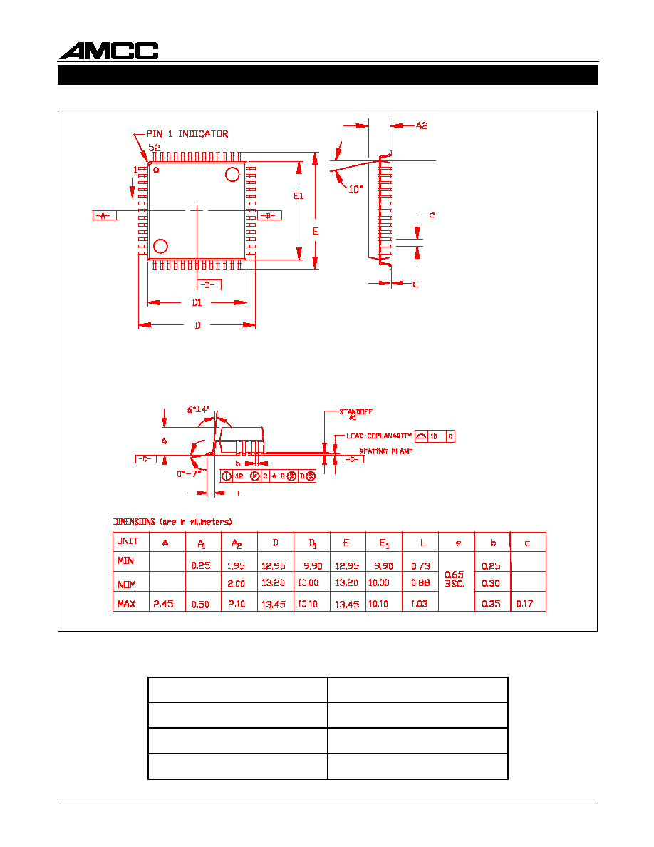
Figure 8. 52 PQFP-HS -- (10mm x 10mm) Plastic Quad Flat Pack
e
c
i
v
e
D
)
r
i
A
l
l
i
t
S
(
a
j
B
6
4
0
2
S
W
/
C
∞
0
5
A
0
5
0
2
S
W
/
C
∞
0
5
3
-
A
0
5
0
2
S
W
/
C
∞
0
5
Table 7. Thermal Management

13
GIGABIT ETHERNET CHIPSET
S2046/S2050
March 29, 2000 / Revision B
Table 8. Absolute Maximum Ratings
The following are the absolute maximum device stress ratings. Stresses beyond those listed may cause
permanent damage to the device. These are stress ratings only. Operation of the device at these or any other
conditions beyond those indicated in the electrical characteristics section of this document is not implied.
Table 9. Recommended Operating Conditions
r
e
t
e
m
a
r
a
P
n
i
M
p
y
T
x
a
M
s
t
i
n
U
s
a
i
B
r
e
d
n
U
e
r
u
t
a
r
e
p
m
e
T
t
n
e
i
b
m
A
0
0
7
C
∞
s
a
i
B
r
e
d
n
U
e
r
u
t
a
r
e
p
m
e
T
n
o
i
t
c
n
u
J
0
3
1
C
∞
D
N
G
o
t
t
c
e
p
s
e
R
h
t
i
w
C
C
V
L
T
T
n
o
e
g
a
t
l
o
V
n
o
i
t
a
r
e
p
O
V
5
n
o
i
t
a
r
e
p
O
V
3
.
3
5
7
.
4
3
1
.
3
0
.
5
3
.
3
5
2
.
5
7
4
.
3
V
V
n
i
P
t
u
p
n
I
L
T
T
y
n
a
n
o
e
g
a
t
l
o
V
0
5
2
.
5
V
D
N
G
o
t
t
c
e
p
s
e
R
h
t
i
w
C
C
V
L
C
E
n
o
e
g
a
t
l
o
V
3
1
.
3
3
.
3
7
4
.
3
V
n
i
P
t
u
p
n
I
L
C
E
P
y
n
a
n
o
e
g
a
t
l
o
V
C
C
V
L
C
E
0
.
2
-
C
C
V
L
C
E
V
Electrostatic Discharge (ESD) Ratings.
The S2046 and S2050 are rated to the following ESD voltages based on the human body model. All
pins are rated above 500 V.
r
e
t
e
m
a
r
a
P
n
i
M
p
y
T
x
a
M
s
t
i
n
U
s
a
i
B
r
e
d
n
U
e
r
u
t
a
r
e
p
m
e
T
e
s
a
C
5
5
-
5
2
1
C
∞
s
a
i
B
r
e
d
n
U
e
r
u
t
a
r
e
p
m
e
T
n
o
i
t
c
n
u
J
5
5
-
0
5
1
C
∞
e
r
u
t
a
r
e
p
m
e
T
e
g
a
r
o
t
S
5
6
-
0
5
1
C
∞
d
n
u
o
r
G
o
t
t
c
e
p
s
e
R
h
t
i
w
C
C
V
n
o
e
g
a
t
l
o
V
5
.
0
-
0
.
7
+
V
n
i
P
t
u
p
n
I
L
T
T
y
n
a
n
o
e
g
a
t
l
o
V
7
.
0
-
C
C
V
V
6
.
+
V
n
i
P
t
u
p
n
I
L
C
E
P
y
n
a
n
o
e
g
a
t
l
o
V
0
C
C
V
L
C
E
V
t
n
e
r
r
u
C
k
n
i
S
t
u
p
t
u
O
L
T
T
8
A
m
t
n
e
r
r
u
C
e
c
r
u
o
S
t
u
p
t
u
O
L
T
T
8
A
m
t
n
e
r
r
u
C
e
c
r
u
o
S
t
u
p
t
u
O
L
C
E
P
d
e
e
p
S
h
g
i
H
0
5
A
m

14
GIGABIT ETHERNET CHIPSET
S2046/S2050
March 29, 2000 / Revision B
Table 10. S2046 DC Characteristics
Table 11. S2050 DC Characteristics
Parameters
Description
Min
Typ
Units
Conditions
VOH
Output HIGH Voltage (TTL)
3.3V Power Supply
3.3V Power Supply
5V Power Supply
2.1
2.2
2.7
2.0
0
--
-500
Max
--
--
--
--
V
V
V
VCC = min, IOH = -2.4mA
VCC = min, IOH = -.1mA
VCC = min, IOH = -1mA
ICC
Supply Current
255
280
mA
Outputs open, VCC = VCC max
PD
Power Dissipation
3.3V Supply
5V Supply
0.91
1.1
1.0
1.2
W
W
Outputs open, VCC = VCC max
Outputs open, VCC = VCC max
VOL
Output LOW Voltage (TTL)
3.3V Power Supply
5V Power Supply
.5
.5
V
V
VCC = min, IOL = 2.4mA
VCC = min, IOL = 4mA
VIH
VIL
IIH
IIL
Input HIGH Voltage (TTL)
Input LOW Voltage (TTL)
Input HIGH Current (TTL)
Input LOW Current (TTL)
--
0.8
50
-50
V
V
µ
A
µ
A
--
VIN = 2.4V
VIN = 0.5V
440
100
1300
--
VINCLK
VDIFF
Single-ended REFCLK input swing
1300
mV
mV
AC coupled
Min. differential input voltage
swing for differential PECL
inputs
Parameters
Description
Min
Typ
Units
Conditions
VOH
Output HIGH Voltage (TTL)
3.3V Power Supply
3.3V Power Supply
5V Power Supply
2.1
2.2
2.7
2.0
0
--
-500
Max
--
--
--
--
V
V
V
VCC = min, IOH = -2.4mA
VCC = min, IOH = -.1mA
VCC = min, IOH = -1mA
ICC
Supply Current
123
160
mA
Outputs open, VCC = VCC max
PD
Power Dissipation
.406
.554
W
Outputs open, VCC = VCC max
VOL
Output LOW Voltage (TTL)
3.3V Power Supply
5V Power Supply
.5
.5
V
V
VCC = min, IOL = 2.4mA
VCC = min, IOL = 4mA
VIH
VIL
IIH
IIL
Input HIGH Voltage (TTL)
Input LOW Voltage (TTL)
Input HIGH Current (TTL)
Input LOW Current (TTL)
0.8
50
-50
V
V
µ
A
µ
A
--
--
VIN = 2.4V
VIN = 0.5V
440
600
--
--
VINCLK
VOUT
Single-ended REFCLK input swing
Serial Output Voltage Swing
1300
1300
mV
mV
AC coupled
50
to VCC -2.0V
15
GIGABIT ETHERNET CHIPSET
S2046/S2050
March 29, 2000 / Revision B
Table 12. Reference Clock Requirements
s
r
e
t
e
m
a
r
a
P
n
o
i
t
p
i
r
c
s
e
D
n
i
M
x
a
M
s
t
i
n
U
s
n
o
i
t
i
d
n
o
C
T
1
K
L
C
F
E
R
.
t
.
r
.
w
p
u
t
e
S
a
t
a
D
0
.
2
-
s
n
.
t
i
B
0
1
1
T
2
K
L
C
F
E
R
.
t
.
r
.
w
d
l
o
H
a
t
a
D
0
.
1
-
s
n
.
t
i
B
0
1
1
T
3
K
L
C
F
E
R
.
t
.
r
.
w
p
u
t
e
S
a
t
a
D
0
.
2
-
s
n
.
t
i
B
0
2
1
T
4
K
L
C
F
E
R
.
t
.
r
.
w
d
l
o
H
a
t
a
D
0
.
2
-
s
n
.
t
i
B
0
2
1
r
e
t
t
i
J
l
a
t
o
T
r
e
t
t
i
J
l
a
t
o
T
t
u
p
t
u
O
a
t
a
D
l
a
i
r
e
S
-
2
9
1
s
p
e
l
p
m
a
s
a
n
o
d
e
t
s
e
t
k
a
e
p
-
o
t
-
k
a
e
P
2
,
s
i
s
a
b
7
.
n
r
e
t
t
a
p
1
≠
T
J
D
t
u
p
t
u
O
a
t
a
D
l
a
i
r
e
S
r
e
t
t
i
J
c
i
t
i
s
n
i
m
r
e
t
e
D
-
0
8
s
p
e
l
p
m
a
s
a
n
o
d
e
t
s
e
t
k
a
e
p
-
o
t
-
k
a
e
P
m
o
d
n
a
R
:
e
t
o
N
.
n
r
e
t
t
a
p
E
L
D
I
,
s
i
s
a
b
e
b
n
a
c
t
u
b
,
d
e
r
u
s
a
e
m
t
o
n
s
i
r
e
t
t
ij
.
p
-
p
s
p
2
1
1
e
b
o
t
d
e
t
a
l
u
c
l
a
c
T
R
D
S
T
,
F
D
S
ll
a
F
d
n
a
e
s
i
R
a
t
a
D
l
a
i
r
e
S
e
m
i
T
-
0
0
3
s
p
e
l
p
m
a
s
a
n
o
d
e
t
s
e
t
%
0
8
o
t
%
0
2
.
s
i
s
a
b
T
N
E
C
N
Y
S
e
m
i
T
ll
a
F
d
n
a
e
s
i
R
N
E
C
N
Y
S
-
0
2
s
n
t
o
n
t
s
u
m
t
u
p
n
i
N
E
C
N
Y
S
f
o
ll
a
f
,
e
s
i
R
.
e
u
l
a
v
s
i
h
t
d
e
e
c
x
e
Table 13. Transmitter Timing
1.
All AC measurements are made from the reference voltage level of the clock (1.4V) to the valid input or output data levels
(.8V or 2.0V).
s
r
e
t
e
m
a
r
a
P
n
o
i
t
p
i
r
c
s
e
D
n
i
M
x
a
M
s
t
i
n
U
s
n
o
i
t
i
d
n
o
C
T
F
6
4
0
2
S
e
c
n
a
r
e
l
o
T
y
c
n
e
u
q
e
r
F
0
0
1
-
0
0
1
+
m
p
p
≠
T
F
0
5
0
2
S
e
c
n
a
r
e
l
o
T
y
c
n
e
u
q
e
r
F
0
0
1
-
0
0
1
+
m
p
p
≠
D
T
2
-
1
y
r
t
e
m
m
y
S
0
4
0
6
%
.
t
p
%
0
5
t
a
e
l
c
y
C
y
t
u
D
T
R
C
R
T
,
F
C
R
e
m
i
T
ll
a
F
d
n
a
e
s
i
R
K
L
C
F
E
R
5
.
0
2
.
3
s
n
%
0
8
-
0
2
≠
r
e
t
t
i
J
m
o
d
n
a
R
-
0
0
1
s
p
k
a
e
P
-
o
t
-
k
a
e
P

16
GIGABIT ETHERNET CHIPSET
S2046/S2050
March 29, 2000 / Revision B
Table 13. Receiver Timing
Note:
All AC measurements are made from the reference voltage level of the clock (1.4V) to the valid input or output data
levels (.8V or 2.0V).
s
r
e
t
e
m
a
r
a
P
n
o
i
t
p
i
r
c
s
e
D
n
i
M
x
a
M
s
t
i
n
U
s
n
o
i
t
i
d
n
o
C
T
p
u
t
r
a
t
S
k
c
o
L
p
u
t
r
a
t
S
t
a
e
m
i
T
k
c
o
L
n
o
i
s
i
u
q
c
A
a
t
a
D
-
5
.
2
s
µ
e
l
p
m
a
s
,
n
r
e
t
t
a
p
E
L
D
I
B
0
1
/
B
8
.
s
i
s
a
b
R
,
R
D
S
R
F
D
S
e
m
i
T
ll
a
F
d
n
a
e
s
i
R
a
t
a
D
t
u
p
n
I
l
a
i
r
e
S
-
0
0
3
s
p
a
n
o
d
e
t
s
e
t
%
0
8
o
t
%
0
2
.
s
i
s
a
b
e
l
p
m
a
s
T
5
w
e
k
S
K
L
C
R
o
t
N
K
L
C
R
5
.
1
-
s
n
T
6
N
K
L
C
R
/
K
L
C
R
.
t
.
r
.
w
p
u
t
e
S
a
t
a
D
5
.
2
-
s
n
.
)
e
t
o
n
e
e
s
(
t
i
B
0
1
T
7
N
K
L
C
R
/
K
L
C
R
.
t
.
r
.
w
d
l
o
H
a
t
a
D
5
.
1
-
s
n
.
)
e
t
o
n
e
e
s
(
t
i
B
0
1
T
8
N
K
L
C
R
.
t
.
r
.
w
p
u
t
e
S
a
t
a
D
1
.
2
-
s
n
.
)
e
t
o
n
e
e
s
(
t
i
B
0
2
T
9
N
K
L
C
R
.
t
.
r
.
w
d
l
o
H
a
t
a
D
3
.
6
-
s
n
.
)
e
t
o
n
e
e
s
(
t
i
B
0
2
T
R
D
e
m
i
T
e
s
i
R
t
u
p
t
u
O
a
t
a
D
-
4
.
2
s
n
.
d
a
o
l
F
p
0
1
,
V
0
.
2
o
t
8
.
0
T
F
D
e
m
i
T
ll
a
F
t
u
p
t
u
O
a
t
a
D
-
4
.
2
s
n
.
d
a
o
l
F
p
0
1
,
V
0
.
2
o
t
8
.
0
T
R
e
m
i
T
e
s
i
R
N
K
L
C
R
/
K
L
C
R
-
0
.
3
s
n
T
F
e
m
i
T
ll
a
F
N
K
L
C
R
/
K
L
C
R
-
0
.
3
s
n
e
l
c
y
C
y
t
u
D
e
l
c
y
C
y
t
u
D
N
K
L
C
R
/
K
L
C
R
0
4
0
6
%
T
J
e
y
e
a
t
a
d
t
u
p
n
I
.
e
c
n
a
r
e
l
o
T
r
e
t
t
i
J
r
o
f
r
e
v
i
e
c
e
r
t
a
n
o
i
t
a
c
o
ll
a
g
n
i
n
e
p
o
.
2
1
-
E
1
R
E
B
9
9
5
s
p
z
3
.
2
0
8
E
E
E
I
n
i
d
e
i
f
i
c
e
p
s
s
A
.
)
9
1
e
r
u
g
i
F
e
e
s
(
T
J
D
.
e
c
n
a
r
e
l
o
T
r
e
t
t
i
J
c
i
t
s
n
i
m
r
e
t
e
D
r
e
t
t
ij
t
u
p
n
i
f
o
t
n
e
n
o
p
m
o
c
c
i
t
s
i
n
i
m
r
e
t
e
D
t
n
e
m
e
r
u
s
a
e
m
e
c
n
a
r
e
l
o
t
r
e
t
t
ij
r
o
f
0
7
3
s
p
z
3
.
2
0
8
E
E
E
I
n
i
d
e
i
f
i
c
e
p
s
s
A
.
)
9
1
e
r
u
g
i
F
e
e
s
(
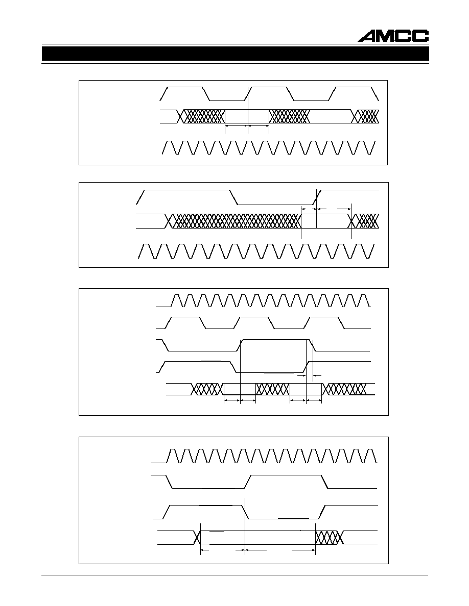
17
GIGABIT ETHERNET CHIPSET
S2046/S2050
March 29, 2000 / Revision B
Figure 11. Transmitter Timing Diagram (10-bit Mode)
D0
2
4
6
8
D10
12
14
16
18
1
3
5
7
D9
11
13
15
17
D19
T1
T2
SERIAL
DATA OUT
REFCLK
D[10:19] 10 BIT DATA
Figure 13. Receiver Timing Diagram (10-bit Mode)
D0
2
4
6
8
D10
12
14
16
18
T5
1
3
5
7
D9
11
13
15
17
D19
T7
T6
T6
K28.5
DATA
T7
REFCLK (125 MHz)
SERIAL DATA IN
RCLK (62.5 MHz)
RCLKN (62.5 MHz)
and SYNC
D[10:19]
Figure 12. Receiver Timing Diagram (20-bit Mode)
D0
2
4
6
8
10
12
14
16
18
1
3
5
7
9
11
13
15
17
D19
T4
T3
SERIAL
DATA OUT
REFCLK
D[0:19]
Figure 14. Receiver Timing Diagram (20-bit Mode)
D0
2
4
6
8
10
12
14
16
18
T8
T9
1
3
5
7
9
11
13
15
17
D19
SERIAL
DATA IN
REFCLK
RCLKN
D[0:19] and SYNC

18
GIGABIT ETHERNET CHIPSET
S2046/S2050
March 29, 2000 / Revision B
Tr
Tf
80%
50%
20%
80%
50%
20%
Backplane
150
150
0.01
µ
F
0.01
µ
F
0.01
µ
F
0.01
µ
F
V
CC
- 0.65 V
100
Tr
Tf
90%
50%
10%
90%
50%
10%
Amplitude
Bit Time
24
%
.10
0
-0.2
0.2
0.3
0.5
0.7
0.8
1.0
1.3
0
.30 .40
.60 .70
.90 1.0
Normalized Time
Normalized Amplitude
Figure 15. Serial Input Rise and Fall Time
Figure 16. Serial Output Load
Figure 17. High Speed Differential Inputs
Figure 18. TTL Input Rise and Fall Time
Figure 19. Receiver Input Eye Diagram Jitter Mask
Figure 20. Acquisition Time Eye Diagram

19
GIGABIT ETHERNET CHIPSET
S2046/S2050
March 29, 2000 / Revision B
Ordering Information
Example:
S2046B-5--S2046 in a 52 PQFP package shipped in trays.
AMCC is a registered trademark of Applied Micro Circuits Corporation.
Copyright Æ 2000 Applied Micro Circuits Corporation
AMCC reserves the right to make changes to its products or to discontinue any semiconductor product or service without notice, and
advises its customers to obtain the latest version of relevant information to verify, before placing orders, that the information being relied
on is current.
AMCC does not assume any liability arising out of the application or use of any product or circuit described herein, neither does it
convey any license under its patent rights nor the rights of others.
AMCC reserves the right to ship devices of higher grade in place of those of lower grade.
AMCC SEMICONDUCTOR PRODUCTS ARE NOT DESIGNED, INTENDED, AUTHORIZED, OR WARRANTED TO BE SUITABLE FOR
USE IN LIFE-SUPPORT APPLICATIONS, DEVICES OR SYSTEMS OR OTHER CRITICAL APPLICATIONS.
Applied Micro Circuits Corporation ∑ 6290 Sequence Dr., San Diego, CA 92121
Phone: (858) 450-9333 ∑ (800)755-2622 ∑ Fax: (858) 450-9885
http://www.amcc.com
C
E
R T I F I E
D
IS
O 9001
E
D
A
R
G
R
E
T
T
I
M
S
N
A
R
T
d
n
a
E
G
A
K
C
A
P
G
N
I
T
A
R
E
G
A
T
L
O
V
G
N
I
P
P
I
H
S
N
O
I
T
A
R
U
G
I
F
N
O
C
l
a
i
c
r
e
m
m
o
C
=
S
6
4
0
2
=
B
R
O
V
5
+
,
P
F
Q
P
2
5
O
/
I
V
3
.
3
+
s
y
a
r
t
=
k
n
a
l
B
k
c
a
p
y
r
d
=
D
/
k
c
a
p
y
r
d
d
n
a
,
l
e
e
r
,
e
p
a
t
=
D
T
/
E
D
A
R
G
R
E
V
I
E
C
E
R
E
G
A
K
C
A
P
G
N
I
P
P
I
H
S
N
O
I
T
A
R
U
G
I
F
N
O
C
l
a
i
c
r
e
m
m
o
C
=
S
0
5
0
2
=
A
=
3
-
A
V
5
+
,
P
F
Q
P
2
5
O
/
I
V
3
.
3
+
R
O
O
/
I
V
3
.
3
+
,
P
F
Q
P
2
5
y
l
n
o
s
y
a
r
t
=
k
n
a
l
B
k
c
a
p
y
r
d
=
D
/
k
c
a
p
y
r
d
d
n
a
,
l
e
e
r
,
e
p
a
t
=
D
T
/
X
XXXX
X
Grade Part No. Package Configuration
X