 | –≠–ª–µ–∫—Ç—Ä–æ–Ω–Ω—ã–π –∫–æ–º–ø–æ–Ω–µ–Ω—Ç: S2061 | –°–∫–∞—á–∞—Ç—å:  PDF PDF  ZIP ZIP |

1
SERIAL BACKPLANE TRANSCEIVER
S2061
February 2, 1999 / Revision C
BiCMOS PECL CLOCK GENERATOR
Æ
DEVICE
SPECIFICATION
SERIAL BACKPLANE TRANSCEIVER
S2061
FEATURES
∑ Transmitter incorporates phase-locked loop
(PLL) providing clock synthesis from low-speed
reference
∑ Receiver PLL configured for clock and data
recovery
∑ 1.0 ≠ 1.25 Gbps operation
∑ 8-bit parallel TTL compatible interface
∑ 1.6W typical power dissipation
∑ +3.3V power supply
∑ Low-jitter serial PECL compatible interface
∑ Lock detect
∑ Local loopback
∑ 64 PQFP/TEP package
∑ Framing performed by receiver
∑ Continuous downstream clocking from receiver
∑ Drives 30m of Twinax cable directly
APPLICATIONS
High-speed data communications
∑ Workstation
∑ Frame buffer
∑ Switched networks
∑ Data broadcast environments
∑ Proprietary extended backplanes
∑ RAID drives
∑ Mass storage devices
GENERAL DESCRIPTION
The S2061 transmitter and receiver chip is designed
to perform high-speed serial data transmission over
fiber optic or coaxial cable interfaces. The chip runs
at data rates from 1.0 to 1.25 Gbps with associated
10-bit data word.
The chip performs parallel-to-serial and serial-to-par-
allel conversion, 8B/10B coding, and framing for
block-encoded data. The transmitter's on-chip PLL
synthesizes the high-speed clock from a low-speed
reference. The receiver's on-chip PLL synchronizes
directly to incoming digital signal to receive the data
stream. The transmitter and receiver each support
differential PECL-compatible I/O for fiber optic com-
ponent interfaces, to minimize crosstalk and maximize
data integrity. Local loopback mode is provided for
system diagnostics.
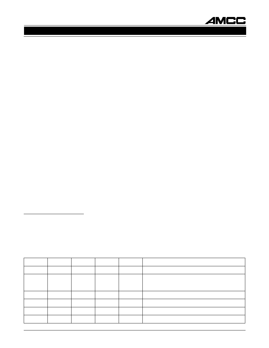
Figure 1 shows a typical configuration incorporating
the chip, which is compatible with AMCC's Crosspoint
switch products.
Figure 1. System Block Diagram
Crosspoint
Switch
S2016(16x16)
S2025(32x32)
S2028(32x32)
MAC
MAC
1000 GBE
OC-3
OC-12
Fibre Channel
0
N
0
N
S2061
MAC
MAC
S2061
S2061
S2061
1000 GBE
OC-3
OC-12
Fibre Channel
1000 GBE
OC-3
OC-12
Fibre Channel
1000 GBE
OC-3
OC-12
Fibre Channel

2
SERIAL BACKPLANE TRANSCEIVER
S2061
February 2, 1999 / Revision C
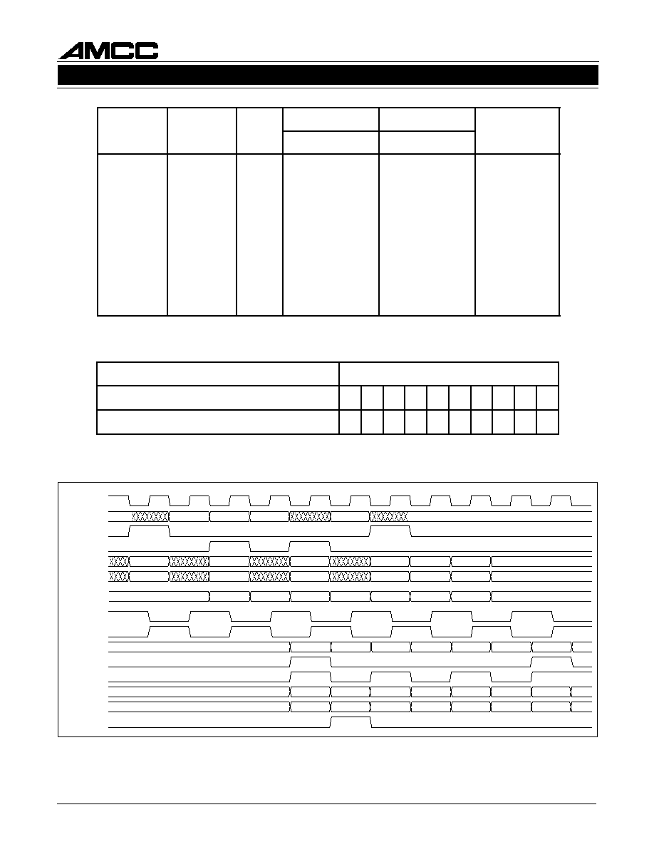
Figure 2. Functional Block Diagram
TXTESTN
TX [0:7]
10
8
PLL CLOCK
MULTIPLIER
F0 = F1 X 10
SHIFT
REGISTER
TXP
TXN
D
Q
PLL CLOCK
RECOVERY
2:1
D
8
D
BITCLK
Q
COM_DET
DETECT
LOGIC
CONTROL
LOGIC
RXP
TBC
RXN
TP
TN
EWRAP
EN_CDET
RX[0:7]
RBC1
RBC0
SHIFT
REGISTER
Input
Latch
8B10B
Encoder
2
TK [0,1]
FRAME
KGEN
WORDCLK
LOCKDET
10
8
8B10B
Decoder
KFLAG
BYTERR
RK[0,1]
SDTTL
SDPECL
FP
S2061 OVERVIEW
The S2061 transceiver performs encoding/decoding
parallel-to-serial and serial-to-parallel conversion and
framing functions to implement a Serial Backplane
interface. Operation of the S2061 chip is straightfor-
ward, as depicted in Figure 2. The sequence of
operations is as follows:
Transmitter
1. 8-bit parallel input
2. 8B/10B encoding
3. Parallel-to-serial conversion
4. Serial output
Receiver
1. Clock and data recovery from serial input
2. Serial-to-parallel conversion
3. Frame detection
4. 10B/8B decoding
5. 8-bit parallel output
Internal clocking and control functions are transparent
to the user. Details of data timing can be seen in Figures
6, 7, 8.
A lock detect feature is provided for the receive PLL.
The LOCKDET output indicates that the PLL is locked
to the data stream.
Loopback Modes
Local loopback mode is supported by the chip. Local
loopback provides capability for performing offline test-
ing of the interface to ensure the integrity of the serial
channel before enabling the transmission medium. It
also allows for system diagnostics. (See the section
Other Operating Modes.)
3
SERIAL BACKPLANE TRANSCEIVER
S2061
February 2, 1999 / Revision C
S2061 TRANSMITTER DESCRIPTION
The S2061 accepts 8-bit parallel input data, performs
8-bit to 10-bit conversion, and serializes the data for
transmission over copper or fiber optic media. The
transmitter can operate in the range of 1.0 GHz to
1.25 GHz, determined by the TBC frequency.
Data Input
Data is input to the S2061 as an 8-bit LVTTL (5V
tolerant) word. Data is latched into an input register
on the rising edge of the input reference clock. The 8-
bit data is 8B/10B coded, and the resultant 10-bit
word is passed to a shift register where it is con-
verted to serial data.
Parallel/Serial Conversion
The parallel-to-serial converter takes 10-bit wide data
from the 8B/10B converter and converts it into a se-
rial bit stream. Data is clocked into the serial output
shift register at a rate that is synchronous to the clock
synthesis unit serial clock. The shift register is clocked
by the internally generated bit clock (10x the TBC
input frequency).
Transmit Byte Clock
The Transmit Byte Clock (TBC) input must be sup-
plied from a clock source with
100 ppm variation.
The internal serial clock is frequency locked to TBC.
To set transmitter operating rate (in the range of 1.0
GHz to 1.25 GHz), the TBC input frequency must be
selected at 1/10 of the desired operating rate (100
MHz to 125 MHz).
8B/10B Coding
The 8B/10B transmission code includes serial encoding
and decoding rules, special characters and error con-
trol. Information is encoded, 8 bits at a time, into a 10-bit
transmission character. The characters defined by this
code ensure that the short run lengths and enough tran-
sitions are present in the serial bit stream to make clock
recovery possible at the receiver. The encoding also
greatly increases the likelihood of detecting any single
or multiple errors that might occur during the transmis-
sion and reception of data. Refer to reference1 for a
complete description of the transmission code.
The 8B/10B transmission code includes D-characters,
used for data transmission, and K-characters, used
for control or protocol functions. Each D-character
and K-character has a positive and a negative parity
version. The parity of each codeword is selected by
the encoder to control the running disparity of the
data stream.
In addition to the 8-bit data input, there are four con-
trol inputs which are used to produce K characters:
FRAME, TK0, TK1, and KGEN. Table 1 shows char-
acter generation based on input states.
K-character generation is controlled using the KGEN
input. When KGEN is asserted, the data on the paral-
lel input is mapped into the corresponding control
character. The parity of the K-character is selected to
minimize running disparity in the serial data stream.
Table 2 lists the K-characters supported by the S2061
and identifies the mapping of the TX[0:7] bits to each
character. Figure 3 shows functional waveforms of
the S2061.
1. A.X. Widner and P.A. Franaszek, "A Byte-Oriented DC Balanced
(0,4) 8B/10B Transmission Code," IBM Research Report RC9391,
May 1982.
E
M
A
R
F
1
K
T
0
K
T
N
E
G
K
]
0
:
7
[
X
T
E
T
A
T
S
1
0
0
0
X
.
d
e
t
a
r
e
n
e
g
y
t
i
r
a
p
s
i
d
g
n
i
n
n
u
R
5
.
8
2
K
0
0
0
1
K
r
e
t
c
a
r
a
h
C
e
u
l
a
V
n
o
e
u
l
a
v
d
e
t
a
r
e
n
e
g
y
t
i
r
a
p
s
i
d
g
n
i
n
n
u
r
f
o
r
e
t
c
a
r
a
h
c
K
.
]
7
:
0
[
D
0
0
1
1
X
.
d
e
t
a
r
e
n
e
g
y
t
i
r
a
p
s
i
d
g
n
i
n
n
u
r
f
o
1
.
8
2
K
0
1
0
1
X
.
d
e
t
a
r
e
n
e
g
y
t
i
r
a
p
s
i
d
g
n
i
n
n
u
r
f
o
3
.
8
2
K
0
1
1
1
X
.
d
e
t
a
r
e
n
e
g
y
t
i
r
a
p
s
i
d
g
n
i
n
n
u
r
f
o
7
.
8
2
K
0
X
X
0
a
t
a
D
.
d
e
t
a
r
e
n
e
g
r
e
t
c
a
r
a
h
c
D
Table 1. Character Generation
4
SERIAL BACKPLANE TRANSCEIVER
S2061
February 2, 1999 / Revision C
Figure 3. Functional Waveform (1250 and 1062.5 Mbit/sec)
REFCLK
FP
RBC1
RBC0
BYTE 1
0
0
K VALUE
BYTE 2
BYTE N
RX[7:0]
TX[7:0]
TK1
K28.5
BYTE 1
K VALUE
BYTE 2
K28.1
BYTE N
K28.5
K28.5
BYTE 1
K VALUE
BYTE 2
K28.1
BYTE N
K28.5
SERIALDATA
FRAME
KGEN
0
0
0
1
TK0
RK0
RK1
BYTE_ERROR
KFLAG
0
0
0
0
0
0
0
0
0
0
0
0
1
0
0
0
K
r
e
t
c
a
r
a
h
C
]
7
:
0
[
X
T
N
E
G
K
+
D
R
t
n
e
r
r
u
C
-
D
R
t
n
e
r
r
u
C
s
t
n
e
m
m
o
C
j
h
g
f
i
e
d
c
b
a
j
h
g
f
i
e
d
c
b
a
0
.
8
2
K
1
.
8
2
K
2
.
8
2
K
3
.
8
2
K
4
.
8
2
K
5
.
8
2
K
6
.
8
2
K
7
.
8
2
K
7
.
3
2
K
5
.
7
2
K
7
.
9
2
K
7
.
0
3
K
0
0
1
1
1
0
0
0
0
0
1
1
1
1
0
0
0
0
1
1
1
0
1
0
0
0
1
1
1
1
1
0
0
0
1
1
1
0
0
1
0
0
1
1
1
1
0
1
0
0
1
1
1
0
1
1
0
0
1
1
1
1
1
1
1
1
1
0
1
1
1
1
1
1
0
1
1
1
1
1
1
0
1
1
1
1
1
1
0
1
1
1
1
1
1
1
1
1
1
1
1
1
1
1
1
1
1
1
1
1
0
1
0
0
0
0
1
1
0
1
1
0
0
0
0
0
1
1
0
1
0
1
0
0
0
0
1
1
0
0
1
1
0
0
0
0
1
1
1
0
1
1
0
0
0
0
1
1
1
0
1
0
0
0
0
0
1
1
1
0
0
1
0
0
0
0
1
1
1
1
1
0
0
0
0
0
1
1
0
0
0
1
0
1
0
1
1
1
0
0
0
1
0
1
1
0
1
1
0
0
0
1
0
1
1
1
0
1
0
0
0
1
0
1
1
1
1
0
0
0
1
0
1
1
1
1
0
0
1
0
0
1
1
1
1
1
0
0
1
0
1
0
1
1
1
1
0
0
1
1
0
0
1
1
1
1
0
0
0
1
0
0
1
1
1
1
0
0
0
1
0
1
1
1
1
1
0
0
0
1
1
0
1
1
1
1
0
0
0
0
0
1
1
1
1
1
0
0
1
1
1
0
1
0
1
0
0
0
1
1
1
0
1
0
0
1
0
0
1
1
1
0
1
0
0
0
1
0
1
1
1
0
1
0
0
0
0
1
r
e
t
c
a
r
a
h
C
c
n
y
S
Table 2. K Character Generation
e
t
y
B
a
t
a
D
]
9
:
0
[
X
R
r
o
]
9
:
0
[
X
T
0
1
2
3
4
5
6
7
8
9
n
o
i
t
a
t
n
e
s
e
r
p
e
R
c
i
r
e
m
u
n
a
h
p
l
A
B
0
1
/
B
8
a
b
c
d
e
i
f
g
h
j
Table 3. 8B/10B Alphabetic Representation

5
SERIAL BACKPLANE TRANSCEIVER
S2061
February 2, 1999 / Revision C
RECEIVER DESCRIPTION
The receiver is designed to implement a Serial
Backplane receiver function through the physical layer.
A block diagram showing the basic function is pro-
vided in Figure 2.
The receiver accepts serial encoded data from a fiber
optic or coaxial interface. Clock recovery is performed
on-chip, with the output data presented as 8-bit paral-
lel data.
Whenever a signal is present, the receiver attempts to
achieve synchronization on both bit and transmission-
word boundaries of the received encoded bit stream.
When bit synchronization is achieved, it is indicated
by the LOCKDET signal. Word synchronization is
achieved by monitoring the incoming serial data stream
for the comma character with negative disparity
(0011111XXX). All K28.5 characters, with the correct
byte alignment, of either disparity will be indicated by
FP. Additional K characters are also decoded per
Table 4. When word synchronization is achieved, the
receiver provides the valid decoded data on its parallel
outputs.
Decoder
The decoder accepts a serial bit stream, does serial to
byte-wide parallel conversion, and performs the 10B/8B
decoding function. The framer recognizes the negative
disparity comma to correctly frame the data.
Byte Synchronization and Framing
The Receiver section performs byte synchronization
on the incoming data stream. Byte synchronization is
performed on only the negative disparity Fibre Chan-
nel comma character (0011111XXX). Thus, in order
to ensure byte synchronization, it is necessary to send
two comma characters in a row to ensure that one of
them is negative disparity. The FP signal will be ac-
tive whenever a K28.5 character of either disparity is
detected. This allows the FRAME input of the trans-
mitter and the FP output on the receiver to be used to
`envelope' the data packet.
recovered clock frequency is determined to be within
approximately 300 ppm and the run length check indi-
cates valid data, the PLL will be declared in lock and the
lock detect output will go active.
In any transfer of PLL control from the serial data to the
reference clock, the RBC1/0 output remains phase
continuous and glitch free assuring the integrity of down-
stream clocking.
Reference Clock Input
The reference clock input must be supplied with a
crystal clock source with 100 PPM tolerance.
OTHER OPERATING MODES
Loopback
When local loopback is enabled, serial data from the
transmitter is internally routed to the receiver, where
the clock is extracted and the data is deserialized. The
parallel data is then sent to the subsystem for verifica-
tion. This loopback mode provides the capability to
perform offline testing of the interface to guarantee the
integrity of the serial channel before enabling the trans-
mission medium. It also allows system diagnostics.
Operating Frequency Range
The S2061 is optimized for operation at 1250 and
1062 Mbit/s. Operation at other rates is possible if the
rate falls between the nominal rates. TBC must be
selected to be within 100 ppm of the desired byte or
word clock rate.
Lock Detect
The S2061 contains a lock detect circuit which monitors
the integrity of the serial data inputs. If the received
serial data fails the run length or frequency test, the PLL
will be forced to lock to the local reference clock. This
will maintain the correct frequency of the RBC1/0 out-
put under loss of signal or loss of lock conditions. If the
serial data inputs have a run length of 80 bit times with
no transitions, the PLL will be declared out of lock. In
addition, if the recovered clock frequency deviates from
the local reference clock frequency by more than ap-
proximately 600 ppm, the PLL will also be declared out
of lock. The lock detect circuit will poll the input data
stream in an attempt to reacquire lock to data. If the
P
F
1
K
R
0
K
R
G
A
L
F
K
E
T
A
T
S
1
0
0
1
.
d
e
t
c
e
t
e
d
5
.
8
2
K
0
0
0
1
.
]
7
:
0
[
X
T
n
o
e
u
l
a
v
,
d
e
t
c
e
t
e
d
r
e
t
c
a
r
a
h
c
K
0
0
1
1
.
d
e
t
c
e
t
e
d
1
.
8
2
K
0
1
0
1
.
d
e
t
c
e
t
e
d
3
.
8
2
K
0
1
1
1
.
d
e
t
c
e
t
e
d
7
.
8
2
K
0
0
0
0
.
r
e
t
c
a
r
a
h
c
D
Table 4. Character Detection
1
1. K characters are detected with either positive or negative disparity.