1
S2065
QUAD SERIAL BACKPLANE DEVICE WITH DUAL I/O
May 19, 2000 / Revision E
S2065
Æ
QUAD SERIAL BACKPLANE DEVICE WITH DUAL I/O
DEVICE
SPECIFICATION
FEATURES
∑ Broad operating rate range
(770 MHz - 1.3 GHz)
- 1062 MHz (Fibre Channel)
- 1250 MHz (Gigabit Ethernet) line rates
- 1/2 Rate Operation
∑ Quad Transmitter incorporating phase-locked
loop (PLL) clock synthesis from low speed
reference
∑ Quad Receiver PLL provides independent clock
and data recovery for each channel
∑ Internally series terminated TTL outputs
∑ On-chip 8B/10B line encoding and decoding for
four separate parallel 8 bit channels
∑ 32 bit parallel TTL interface
∑ Low-jitter serial PECL interface
∑ Local Loopback
∑ Interfaces with coax, twinax, or fiber optics
∑ Single +3.3V supply, 2.7 W Power dissipation
∑ Compact 23mm x 23mm 208 TBGA package
∑ Redundant high speed transmit and receive
serial interfaces
APPLICATIONS
High-speed data communications
∑ Ethernet Backbones
∑ Workstation
∑ Frame buffer
∑ Switched networks
∑ Data broadcast environments
∑ Proprietary extended backplanes
GENERAL DESCRIPTION
The S2065 facilitates high-speed serial transmission
of data in a variety of applications including Gigabit
Ethernet, Fibre Channel, serial backplanes, and pro-
prietary point to point links. The chip provides four
separate transceivers which can be operated indi-
vidually or locked together for an aggregate data ca-
pacity of >4 Gbit/sec in each direction. The S2065
provides dual transmit and receive serial I/O. The
dual transmit and receive serial I/O are useful for
backbone applications in which redundant optical or
electrical links are required.
Each bi-directional channel provides 8B/10B coding/
decoding, parallel to serial and serial to parallel con-
version, clock generation/recovery, and framing. The
on-chip transmit PLL synthesizes the high-speed
clock from a low-speed reference. The on-chip quad
receive PLL is used for clock recovery and data re-
timing on the four independent data inputs. The
transmitter and receiver each support differential
PECL-compatible I/O for copper or fiber optic com-
ponent interfaces with excellent signal integrity. Re-
dundant transmit and receive serial I/O are provided
to support applications with redundant switch fabrics
or line interfaces. Local loopback mode allows for
system diagnostics. The chip requires a 3.3V power
supply and dissipates approximately 2.7 watts.
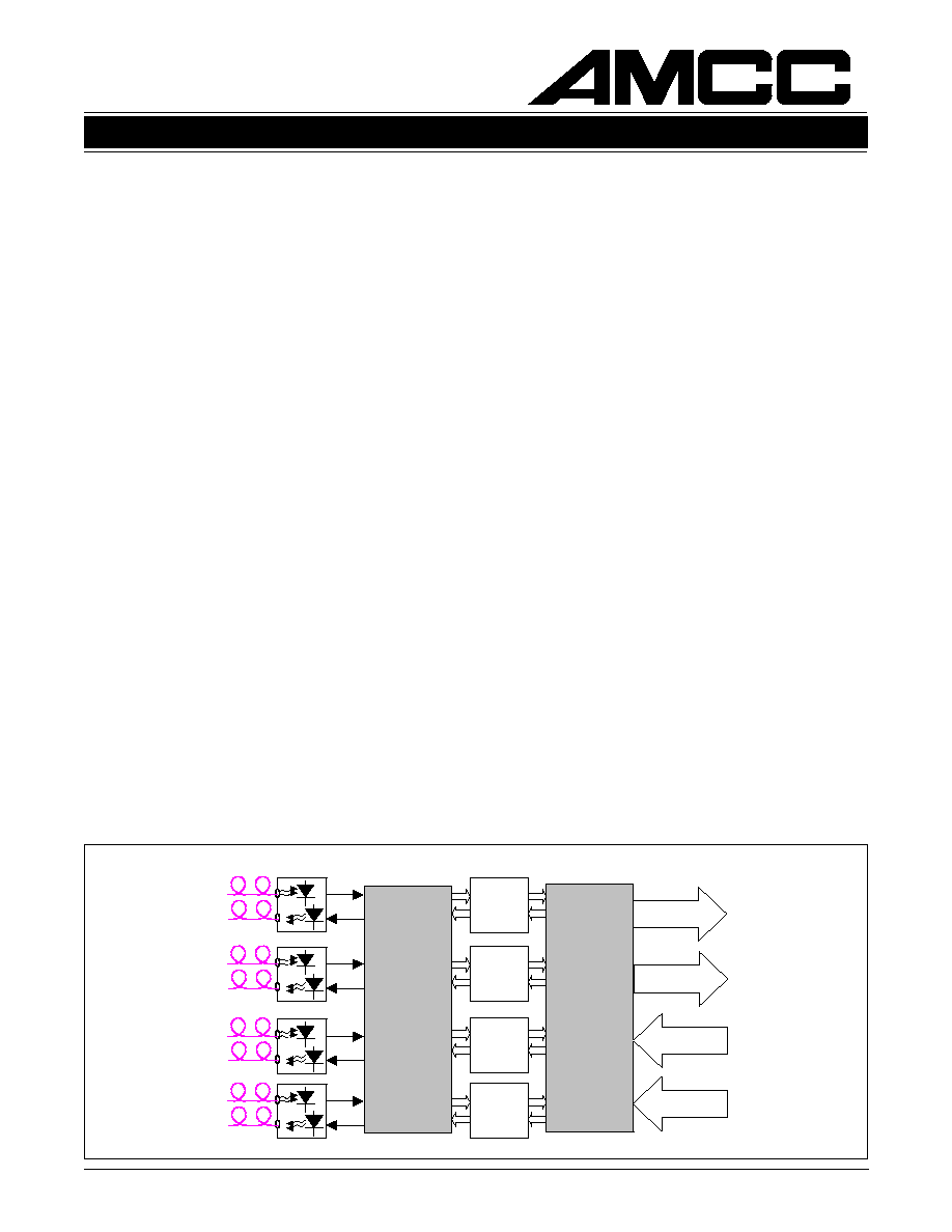
Figure 1 shows the use of the S2065 and S2066 in a
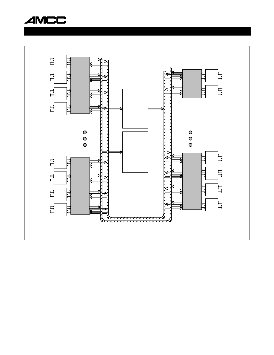
Gigabit Ethernet application. Figure 2 shows the use of
a S2065 in a serial backplane application. Figure 3
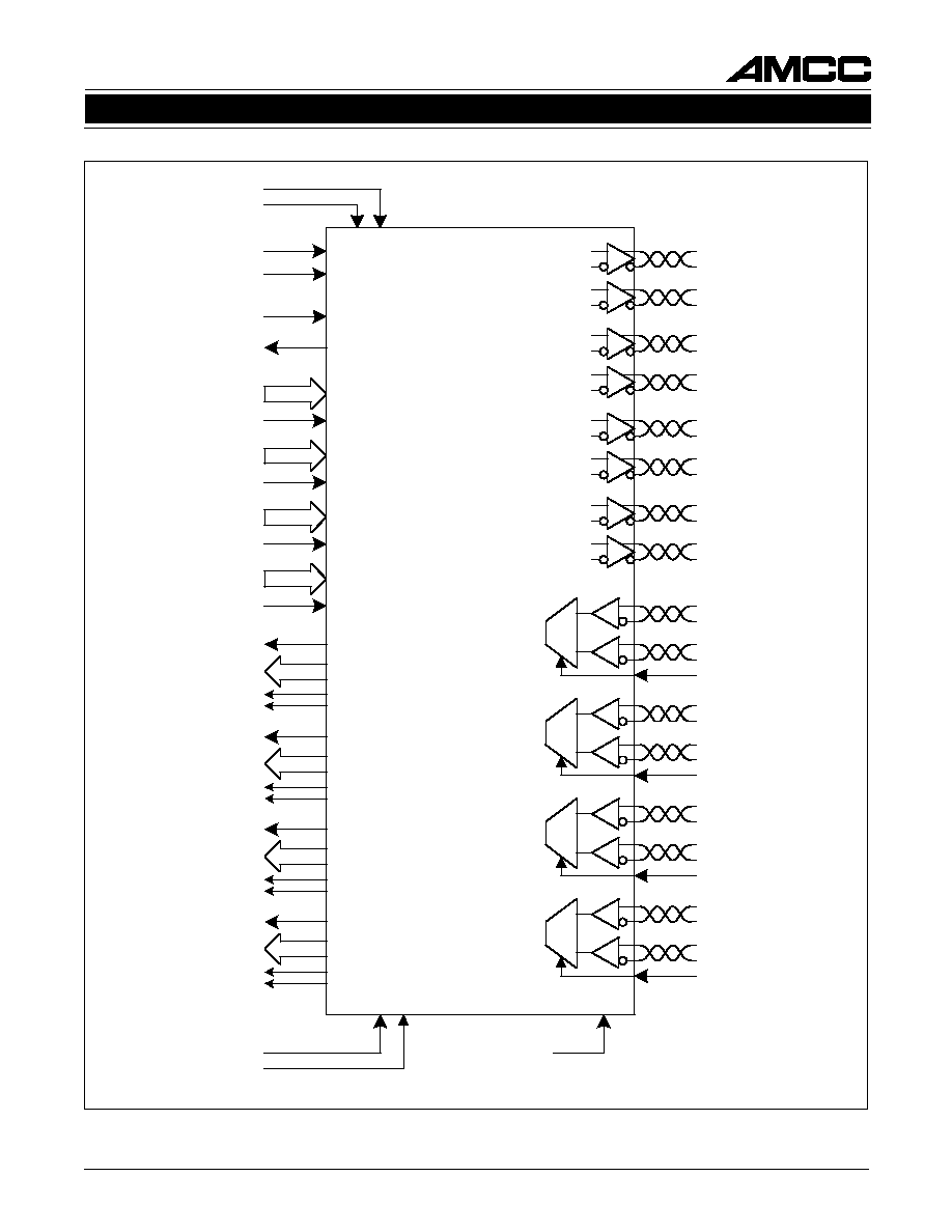
summarizes the input and output signals on the S2065.
Figures 4 and 5 show the transmit and receive block
diagrams, respectively.
Figure 1. Typical Quad Gigabit Ethernet Application
MAC
(ASIC)
QUAD
GIGABIT
ETHERNET
INTERFACE
MAC
(ASIC)
MAC
(ASIC)
MAC
(ASIC)
TO SERIAL BACKPLANE
GE INTERFACE
SERIAL BP DRIVER
TO SERIAL BACKPLANE
S2066
S2065
2
S2065
QUAD SERIAL BACKPLANE DEVICE WITH DUAL I/O
May 19, 2000 / Revision E
Figure 2. Typical Backplane Application
MAC
(ASIC)
S2065
ATM
Fibre
Channel
Ethernet
etc.
MAC
(ASIC)
MAC
(ASIC)
MAC
(ASIC)
Crosspoint
Switch #2
S2016
S2025
S2028
Crosspoint
Switch #1
S2016
S2025
S2028
MAC
(ASIC)
S2065
ATM
Fibre
Channel
Ethernet
etc.
MAC
(ASIC)
MAC
(ASIC)
MAC
(ASIC)
MAC
(ASIC)
S2065
ATM
Fibre
Channel
Ethernet
etc.
MAC
(ASIC)
MAC
(ASIC)
MAC
(ASIC)
MAC
(ASIC)
S2067
ATM
Fibre
Channel
Ethernet
etc.
MAC
(ASIC)
BACKPLANE SIGNAL GROUP #1
BACKPLANE SIGNAL GROUP #2