1
S2068
DUAL GIGABIT ETHERNET TRANSCEIVER
June 20, 2000 / Revision B
S2068
Æ
DUAL GIGABIT ETHERNET TRANSCEIVER
DEVICE
SPECIFICATION
FEATURES
∑ Functionally compliant with IEEE 802.3z Gigabit
Ethernet Applications
∑ 1250 MHz (Gigabit Ethernet) operating rate
≠ Half rate operation
∑ Dual Transmitter incorporating phase-locked
loop (PLL) clock synthesis from low speed
reference
∑ Dual Receiver PLL provides clock and data
recovery
∑ Internally series terminated TTL outputs
∑ Low-jitter serial PECL interface
∑ Local Loopback
∑ Interfaces with coax, twinax, or fiber optics
∑ Single +3.3V supply, 1.37W power dissipation
∑ Compact 21mm x 21mm 156 TBGA package
APPLICATIONS
High-speed data communications
∑ Ethernet Backbones
∑ Multi-port Gigabit Ethernet Cards
∑ Switched networks
∑ Data broadcast environments
GENERAL DESCRIPTION
The S2068 dual transmitter and receiver chip is de-
signed to provide two channels of high-speed serial
data transmission over fiber optic or copper interfaces
conforming to the requirements of the IEEE 802.3z
Gigabit Ethernet specification. The chip runs at
1250.0 Mbps serial data rate with an associated
10-bit parallel data word. The chip provides two sepa-
rate receive PLLs which can be operated
asyncronously at slightly different frequencies.
Each bi-directional channel provides parallel to serial
and serial-to-parallel conversion, clock generation
and recovery, and framing. The on-chip transmit PLL
synthesizes the high-speed clock from a low-speed
reference. The on-chip dual receive PLL is used for
clock recovery and data re-timing on the two inde-
pendent data inputs. The transmitter and receiver
each support differential PECL-compatible I/O for
copper or fiber optic component interfaces and pro-
vide excellent signal integrity. Local loopback mode
allows for system diagnostics. The chip requires a
3.3V power supply and dissipates 1.37 watts.
Figure 1 shows the use of the S2062 and S2068 in a
Gigabit Ethernet application. Figure 2 summarizes
the input/output signals of the device. Figures 3 and
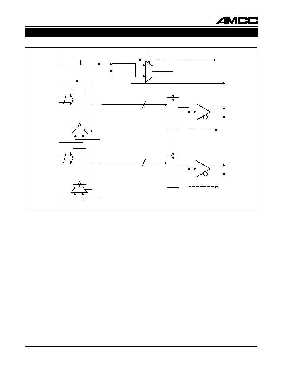
4 show the transmit and receive block diagrams, re-
spectively.
Figure 1. Typical Dual Gigabit Ethernet Application
MAC
(ASIC)
S2062
DUAL
GIGABIT
ETHERNET
INTERFACE
MAC
(ASIC)
TO SERIAL
BACKPLANE
S2068
GE INTERFACE
SERIAL BP DRIVER
5
S2068
DUAL GIGABIT ETHERNET TRANSCEIVER
June 20, 2000 / Revision B
TRANSMITTER DESCRIPTION
The transmitter section of the S2068 contains a
single PLL which is used to generate the serial rate
transmit clock for all transmitters. Transmitter
functionalities shown schematically in Figure 3. Two
channels are provided with a variety of options re-
garding input clocking and loopback. The transmit-
ters operate at 1.250 GHz, 10 or 20 times the
reference clock frequency.
Data Input
The S2068 has been designed to simplify the paral-
lel interface data transfer and provides flexibility in
the clocking of parallel data. Prior implementations
of this function have either forced the user to syn-
chronize transmit data to the reference clock or to
provide the output clock as a reference to the PLL,
resulting in increased jitter at the serial interface.
The S2068 incorporates a unique FIFO structure
which enables the user to provide a "clean" refer-
ence source for the PLL and to accept a separate
external clock which is used exclusively to reliably
clock data into the device.
The S2068 also provides a system clock output,
TCLKO, which is derived from the internal VCO. The
frequency of this output is constant at the parallel
word rate, 1/10 the serial data rate, regardless of
whether the reference is provided at 1/10 or 1/20 the
serial data rate. This clock can be used by upstream
circuitry as a system clock. See Table 1.
Data to be input to the S2068 should be coded to
ensure transition density and DC balance. Data is
input to each channel of the S2068 as a 10 bit wide
word. An input FIFO and a clock input, TBCx, are
provided for each channel of the S2068. This device
can operate in two different modes. The S2068 can
be configured to use either the TBCx (TBC MODE)
input or the REFCLK input (REFCLK MODE). Table
2 provides a summary of the input modes for the
S2068.
Operation in the TBC MODE makes it easier for us-
ers to meet the relatively narrow setup and hold time
window required by the 125 Mbit/sec 10 bit interface.
The TBC signal is used to clock the data into an
internal holding register and the S2068 synchronizes
its internal data flow to ensure stable operation.
REFCLK, not TBCx, is used as the reference for the
transmit PLL. This ensures minimum jitter on the
E
T
A
R
L
E
S
K
L
C
K
L
C
F
E
R
y
c
n
e
u
q
e
r
F
t
u
p
t
u
O
l
a
i
r
e
S
e
t
a
R
0
K
L
C
T
y
c
n
e
u
q
e
r
F
0
0
0
1
/
R
D
S
s
p
b
M
0
5
2
1
0
1
/
R
D
S
0
1
0
2
/
R
D
S
s
p
b
M
0
5
2
1
0
1
/
R
D
S
1
0
0
1
/
R
D
S
s
p
b
M
5
2
6
0
1
/
R
D
S
1
1
0
2
/
R
D
S
s
p
b
M
5
2
6
0
1
/
R
D
S
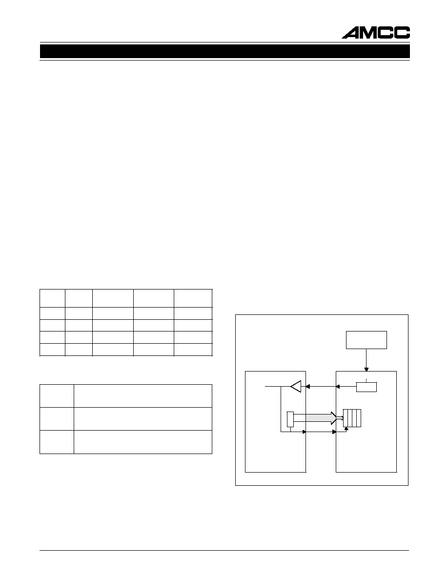
Table 1. Operating Rates
REFCLK
S2068
125 MHz or 62.5 MHz
TBCx
DINx[0:9]
REF
OSCILLATOR
MAC
ASIC
TCLKO
PLL
Figure 5. DIN Clocking with TBC
Note that internal synchronization of FIFOs is performed upon
de-assertion of RESET.
E
D
O
M
T
n
o
i
t
a
r
e
p
O
0
a
t
a
d
k
c
o
l
c
o
t
d
e
s
u
K
L
C
F
E
R
.
e
d
o
M
K
L
C
F
E
R
.
s
l
e
n
n
a
h
c
ll
a
r
o
f
s
O
F
I
F
o
t
n
i
1
s
O
F
I
F
o
t
n
i
a
t
a
d
k
c
o
l
c
o
t
d
e
s
u
x
C
B
T
.
e
d
o
M
C
B
T
.
s
l
e
n
n
a
h
c
ll
a
r
o
f
Table 2. Input Modes
Note: SDR = Serial Data Rate.