 | –≠–ª–µ–∫—Ç—Ä–æ–Ω–Ω—ã–π –∫–æ–º–ø–æ–Ω–µ–Ω—Ç: S2072 | –°–∫–∞—á–∞—Ç—å:  PDF PDF  ZIP ZIP |
1
FOUR PORT BYPASS AND REPEATER FOR FC-AL
S2072
February 18, 2000 / Revision D
Æ
FEATURES
∑
Micropower Bipolar Technology
∑ ANSI X3T11 Fibre Channel Compliant
∑ Monolithic Clock Recovery Unit
≠ Retimes & Buffers Received Data
≠ Jitter Peaking < 0.1 dB
∑ Lock Detect Function
≠ Frequency Detection
∑ Four Port Bypass Circuits
∑ Suitable for both Coaxial and Optical Link
∑ Low Power Operation 0.93 W Typical
∑ 106.25 or 53.125 MHz Reference Clock
∑
Compact 10 mm x 10 mm 64 Pin
PQFP Package
∑ 3.3 V Supply
APPLICATIONS
∑ FC-AL Nodes
∑ RAID
∑
JBOD
∑ SAN
GENERAL DESCRIPTION
The Four Port Bypass and Repeater for FC-AL Cir-
cuit is used in full-speed (1.0625 Gb/s) Disk Arrays.
It contains a monolithic Clock Recovery Unit (CRU),
a lock detect feature and four port bypass circuits.
The S2072 may be used to implement a single chip
Arbitrated Loop Port Bypass Retiming Node. The
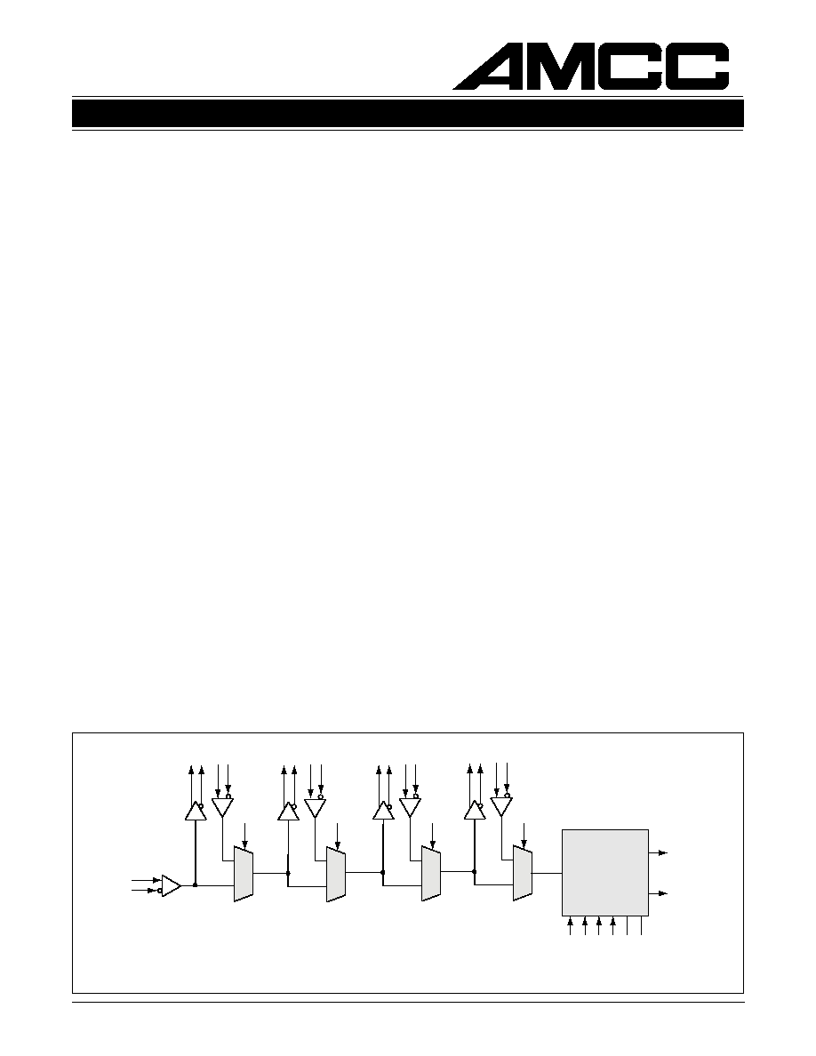
Figure 1. S2072 Functional Block Diagram
DEVICE
SPECIFICATION
FOUR PORT BYPASS AND REPEATER FOR FC-AL
S2072
S2072 performs the function of four port bypass cir-
cuits followed by a Clock and Data Retimer (CDR).
The CDR retimes incoming serial data, detects
whether a valid signal is present and outputs a low
jitter serial data stream.
FUNCTIONAL DESCRIPTION
The S2072 functional block diagram is shown in Fig-
ure 1. The S2072 performs two functions. The first
function is a Quad Port Bypass Circuit (PBC) for
nodes in a FC-AL system. The low jitter accumula-
tion of the port bypass path is essential in these
systems. The second function is to restore signal
quality in RAID drives using the FC-AL link configu-
ration. The S2072 clock and data recovery PLL pro-
vides low jitter transfer peaking and high jitter
tolerance. In addition, the lock detect circuit monitors
the incoming signals for frequency, which is useful
for link performance monitoring and detection of
channel present.
Jitter Performance
Input jitter tolerance is defined as the amplitude of
frequency dependent, random and deterministic jitter
that causes the clock recovery PLL to violate the
BER specifications.
The S2072 complies with the minimum jitter toler-
ance requirements proposed by the Fibre Channel
jitter working group when used with differential in-
puts and outputs as shown in Figure 2. In addition,
the S2072 is designed for minimum jitter generation
and jitter transfer specifications. This allows the opti-
mum system design for arbitrated loop architectures.
0
1
0
1
0
1
0
1
DDO0 DDI0
EN0
DDO1
DDI1
EN1
DDO2
DDI2
EN2
DDO3 DDI3
EN3
IN
CDR
OUTP/N
LOCKDET
BYPASS
REFCLK
LCKREFN
REFSEL
LPF1
LPF2

2
FOUR PORT BYPASS AND REPEATER FOR FC-AL
S2072
February 18, 2000 / Revision D
Figure 2. FC-AL JBOD Application for Repeaters
CDR
0
1
0
1
0
1
0
1
Disk
Storage
FC-AL Disk Drive
LRC
Interlock
S2070
FC
XCVR
E_STORE
Disk
Storage
FC-AL Disk Drive
LRC
Interlock
E_STORE
Disk
Storage
FC-AL Disk Drive
LRC
Interlock
E_STORE
Optics
or
Copper
S2058
S2072
Dual
SC
or
DB-9
Normal
Normal
Normal
Bypass
Pulldown for Bypass in
Absence of Disk Drive
S2070
FC
XCVR
S2070
FC
XCVR

3
FOUR PORT BYPASS AND REPEATER FOR FC-AL
S2072
February 18, 2000 / Revision D
DEVICE DESCRIPTION
The S2072 provides a port bypass function for up to 4
nodes in an FC-AL circuit, with low jitter accumulation.
An integrated repeater reduces jitter and restores sig-
nal amplitude levels for optimal signal integrity. Jitter
performance of the PLL is specified by jitter tolerance
and jitter transfer. In accordance with ANSI X3T11,
jitter tolerance is divided into random, deterministic,
and frequency dependent jitter. Figure 3 illustrates the
components of random, deterministic, and frequency
dependent jitter that must be tolerated to be ANSI
X3T11 compliant.
Frequency Dependent Jitter Tolerance
Frequency Dependent Input jitter tolerance is defined
as the peak to peak amplitude of sinusoidal jitter ap-
plied on the input signal that causes the clock recovery
to violate BER specifications. See Figure 4.
Random Jitter Tolerance
Random Jitter Tolerance is the amount of jitter with a
gaussian distribution that the clock recovery PLL must
tolerate.
Deterministic Jitter Tolerance
Deterministic Jitter Tolerance is the amount of Deter-
ministic jitter that the clock recovery PLL must tolerate.
Jitter transfer
Jitter transfer is defined as the ratio of jitter on the
output signal to the jitter applied on the input signal
versus frequency. Jitter transfer requirements are
shown in Figures 4 and 5. The measurement condition
is that input sinusoidal jitter up to the mask level in
Figure 4 is applied and the output jitter is measured for
compliance to the mask of Figure 5. The jitter transfer
mask includes specifications for both jitter peaking and
bandwidth.
Lock detect
The S2072 lock detect circuit monitors the selected
input signal to detect the presence of the channel. This
is done by monitoring the frequency content of the in-
coming data. The frequency monitor circuit checks the
difference between the divided down recovered clock
and the externally supplied reference clock (REFCLK).
If the frequency difference between the recovered
clock and the reference clock varies by more than
±
100 ppm the part will be declared out of lock. In the out
of lock state, the PLL will lock to the local reference
clock and periodically poll the serial data inputs looking
for data with valid frequency content.
Figure 3. Input Jitter Tolerance
Figure 5. Jitter Transfer Specification
Figure 4. Frequency Dependent Jitter
Tolerance Mask
FREQ DEP
DJ(ISI)
RJ
10
-12
0
329
612
940
PS
BER
f
c
/25,000
(42.5 kHz)
Cut-off Freq A
f
c
/1,667
(637 kHz)
Cut-off Freq B
TIME (Unit Interval - UI)
1.5
0.4
Frequency (Hz)
(kHz) = Cut-off Freq @ 1,0625 Gbps
Jitter
Transfer
Acceptable Range
slope = -20 dB/decade
fc = 2 MHz
Peaking = 0.2 dB

4
FOUR PORT BYPASS AND REPEATER FOR FC-AL
S2072
February 18, 2000 / Revision D
Table 1. Pin Assignment and Descriptions
e
m
a
N
n
i
P
l
e
v
e
L
O
/
I
#
n
i
P
n
o
i
t
p
i
r
c
s
e
D
P
T
U
O
N
T
U
O
.
f
f
i
D
L
C
E
P
V
L
O
8
3
9
3
e
e
S
(
.
p
o
o
l
e
h
t
n
i
C
B
P
t
x
e
n
e
h
t
o
t
d
e
t
c
e
n
n
o
c
e
b
o
t
t
u
p
t
u
o
l
a
i
r
e
S
a
t
a
d
d
n
a
k
c
o
l
c
e
h
t
y
b
d
e
m
i
t
e
r
n
e
e
b
s
a
h
t
u
p
t
u
o
s
i
h
T
)
.
2
e
r
u
g
i
F
.
L
L
P
y
r
e
v
o
c
e
r
P
N
I
N
N
I
.
f
f
i
D
L
C
E
P
V
L
I
6
1
5
1
.
t
i
u
c
r
i
C
s
s
a
p
y
B
t
r
o
P
s
u
o
i
v
e
r
p
e
h
t
m
o
r
f
t
u
p
n
i
l
a
i
r
e
S
P
0
I
D
D
N
0
I
D
D
P
1
I
D
D
N
1
I
D
D
P
2
I
D
D
N
2
I
D
D
P
3
I
D
D
N
3
I
D
D
.
f
f
i
D
L
C
E
P
V
L
I
4
3
1
6
0
6
0
5
9
4
3
4
2
4
y
b
n
e
v
i
r
d
e
b
d
l
u
o
h
s
t
u
p
n
i
s
i
h
T
.
s
s
a
p
y
b
t
r
o
p
e
h
t
o
t
t
u
p
n
i
l
a
i
r
e
S
f
o
e
n
o
y
n
A
.
s
s
a
p
y
b
t
r
o
p
e
h
t
o
t
d
e
t
c
e
n
n
o
c
e
v
i
r
d
k
s
i
d
L
A
-
C
F
e
h
t
n
i
s
i
C
B
P
s
t
i
f
i
k
c
o
l
b
R
D
C
e
h
t
o
t
d
e
t
u
o
r
e
b
y
a
m
s
r
i
a
p
t
u
p
n
i
e
s
e
h
t
.
e
d
o
M
s
s
a
p
y
B
t
r
o
P
n
i
e
r
a
s
C
B
P
r
e
h
t
o
e
h
t
d
n
a
e
d
o
M
l
a
m
r
o
N
K
L
C
F
E
R
L
T
T
I
9
2
.
e
v
i
t
c
a
e
g
d
e
g
n
i
s
i
r
,
L
L
P
e
h
t
r
o
f
k
c
o
l
c
e
c
n
e
r
e
f
e
R
1
F
P
L
2
F
P
L
g
o
l
a
n
A
2
3
3
3
s
r
o
t
s
i
s
e
r
d
n
a
r
o
t
i
c
a
p
a
c
r
e
t
li
f
p
o
o
l
l
a
n
r
e
t
x
e
e
h
T
.
s
n
i
p
r
e
t
li
F
p
o
o
L
.
s
n
i
p
e
s
e
h
t
o
t
d
e
t
c
e
n
n
o
c
e
r
a
N
F
E
R
K
C
L
e
t
a
t
S
3
L
T
T
I
5
3
e
h
t
o
t
k
c
o
l
o
t
d
e
c
r
o
f
e
b
ll
i
w
L
L
P
e
h
t
,
e
v
i
t
c
a
n
e
h
W
.
w
o
L
e
v
i
t
c
A
.
)
K
L
C
F
E
R
(
k
c
o
l
c
e
c
n
e
r
e
f
e
r
l
a
c
o
l
T
E
D
K
C
O
L
L
T
T
O
4
3
d
e
k
c
o
l
s
i
L
L
P
e
h
t
s
e
t
a
c
i
d
n
i
T
E
D
K
C
O
L
,
e
v
i
t
c
a
n
e
h
W
.
h
g
i
H
e
v
i
t
c
A
e
h
t
o
t
k
c
o
l
ll
i
w
L
L
P
e
h
t
,
e
v
i
t
c
a
n
i
n
e
h
W
.
m
a
e
r
t
s
a
t
a
d
l
a
i
r
e
s
e
h
t
o
t
.
n
o
i
t
i
d
n
o
c
a
t
a
d
f
o
s
s
o
l
a
g
n
i
t
a
c
i
d
n
i
k
c
o
l
c
e
c
n
e
r
e
f
e
r
l
a
c
o
l
P
0
O
D
D
N
0
O
D
D
P
1
O
D
D
N
1
O
D
D
P
2
O
D
D
N
2
O
D
D
P
3
O
D
D
N
3
O
D
D
.
f
f
i
D
L
C
E
P
V
L
O
3
1
2
1
4
6
3
6
8
5
7
5
6
4
5
4
t
u
p
n
i
e
h
t
e
v
i
r
d
d
l
u
o
h
s
s
t
u
p
t
u
o
e
s
e
h
T
.
s
r
i
a
p
t
u
p
t
u
o
s
s
a
p
y
b
t
r
o
P
.
e
v
i
r
d
k
s
i
d
L
A
-
C
F
e
h
t
f
o
s
t
r
o
p
0
N
E
1
N
E
2
N
E
3
N
E
L
T
T
I
2
2
3
2
5
2
6
2
t
r
o
p
e
h
t
,
e
v
i
t
c
a
n
i
s
i
N
E
n
e
h
W
.
h
g
i
H
e
v
i
t
c
A
.
l
o
r
t
n
o
c
s
s
a
p
y
b
t
r
o
P
s
s
a
p
y
b
t
r
o
p
,
e
v
i
t
c
a
s
i
N
E
n
e
h
W
.
e
d
o
m
s
s
a
p
y
b
n
i
e
b
ll
i
w
s
s
a
p
y
b
.
e
d
o
m
l
a
m
r
o
n
n
i
e
b
ll
i
w

5
FOUR PORT BYPASS AND REPEATER FOR FC-AL
S2072
February 18, 2000 / Revision D
e
m
a
N
n
i
P
l
e
v
e
L
O
/
I
#
n
i
P
n
o
i
t
p
i
r
c
s
e
D
D
N
G
d
n
u
o
r
G
,
0
2
,
4
1
,
1
,
7
3
,
0
3
9
5
,
8
4
e
r
a
d
n
a
e
c
a
f
r
u
s
e
i
d
e
h
t
o
t
d
e
t
n
u
o
m
y
ll
a
c
i
s
y
h
p
e
r
a
s
n
i
p
d
n
u
o
r
G
l
a
m
r
e
h
t
t
s
e
b
r
o
F
.
h
t
a
p
l
a
m
r
e
h
t
e
h
t
f
o
t
r
a
p
t
n
a
t
r
o
p
m
i
n
a
d
n
u
o
r
g
a
o
t
d
e
t
c
e
n
n
o
c
e
b
d
l
u
o
h
s
s
n
i
p
d
n
u
o
r
g
ll
a
,
e
c
n
a
m
r
o
f
r
e
p
.
e
l
b
i
s
s
o
p
f
i
s
a
i
v
e
l
p
i
t
l
u
m
g
n
i
s
u
e
n
a
l
p
C
C
V
,
0
4
,
1
1
,
2
,
4
4
,
1
4
2
6
,
7
4
.
y
l
p
p
u
s
r
e
w
o
P
V
3
.
3
+
A
C
C
V
g
o
l
a
n
A
9
1
8
2
.
R
D
C
e
h
t
r
o
f
y
l
p
p
u
s
r
e
w
o
P
V
3
.
3
+
A
D
N
G
g
o
l
a
n
A
8
1
7
2
.
R
D
C
e
h
t
r
o
f
d
n
u
o
r
G
S
S
A
P
Y
B
l
e
v
e
L
3
L
T
T
I
7
1
n
o
i
t
a
r
e
p
o
p
i
h
c
l
a
m
r
o
N
.
t
s
e
t
g
n
i
r
u
t
c
a
f
u
n
a
m
r
o
f
d
e
s
U
.
h
g
i
H
e
v
i
t
c
A
e
h
t
d
n
a
e
d
o
M
t
s
e
T
n
i
t
u
p
s
i
2
7
0
2
S
,
e
v
i
t
c
a
n
e
h
W
.
e
v
i
t
c
a
n
i
n
e
h
w
.
g
n
i
t
s
e
t
y
r
o
t
c
a
f
r
o
f
d
e
s
s
a
p
y
b
e
b
ll
i
w
L
L
P
L
E
S
F
E
R
L
T
T
I
6
3
z
H
M
5
2
.
6
0
1
s
w
o
ll
a
,
e
v
i
t
c
a
s
i
L
E
S
F
E
R
n
e
h
W
.
w
o
L
e
v
i
t
c
A
z
H
M
5
2
1
.
3
5
s
w
o
ll
a
,
e
v
i
t
c
a
n
i
s
i
L
E
S
F
E
R
n
e
h
W
.
k
c
o
l
c
e
c
n
e
r
e
f
e
r
.
k
c
o
l
c
C
N
D
,
8
,
7
,
6
,
5
,
1
2
,
0
1
,
9
,
1
3
,
4
2
,
2
5
,
1
5
,
4
5
,
3
5
6
5
,
5
5
.
t
c
e
n
n
o
c
t
o
n
o
D
Table 1. Pin Assignment and Descriptions