 | –≠–ª–µ–∫—Ç—Ä–æ–Ω–Ω—ã–π –∫–æ–º–ø–æ–Ω–µ–Ω—Ç: S2075A | –°–∫–∞—á–∞—Ç—å:  PDF PDF  ZIP ZIP |

1
S2075
FIBRE CHANNEL BIT STREAM MONITOR WITH REPEATER
May 15, 2000 / Revision A
S2075
Æ
DEVICE SPECIFICATION
FIBRE CHANNEL BIT STREAM MONITOR WITH REPEATER
FEATURES
∑ Repeater with parallel monitor function
∑ Selectable parallel input provides local control
of serial bit stream
∑ 1062MHz (Fibre Channel) line rates
∑ Half and full VCO output rates
∑ Functionally compliant ANSI X3T11 Fibre
Channel Specification
∑ TTL Bypass Select
∑ Transmitter incorporating phase-locked loop
(PLL) clock synthesis from low speed reference
∑ Repeater PLL provides clock and data recovery
∑ 10 bit parallel TTL compatible interface
∑ Low-jitter serial LVPECL compatible interface
∑ Local loopback
∑ Single +3.3V supply, 600 mW power dissipation
∑ 64 PQFP package
∑ Continuous downstream clocking from
parallel output
∑ Drives 30m of Twinax cable directly
APPLICATIONS
∑ Storage area network
∑ Workstation
∑ Frame buffer
Figure 1. System Block Diagram
S2075
Local
Controller
Serial Bit Stream
Serial Bit Stream
Parallel
Input
(Transceiver
Mode)
Parallel
Output
(Monitor)
PBCSEL
∑ Switched networks
∑ Data broadcast environments
∑ Proprietary extended backplanes
GENERAL DESCRIPTION
The S2075 bit stream monitor with repeater facili-
tates high speed serial transmission of data over fi-
ber optic, coax, or twinax interfaces. The device
conforms to the requirements of the ANSI X3T11
Fibre Channel specification, and runs at 1062 Mbps
data rates with an associated 10-bit data word.
The chip provides a repeater function with serial-to-
parallel conversion for monitoring the serial bit
stream. An on-chip PLL performs clock recovery and
data retiming of the serial bit stream. In transceiver
mode, parallel data from the local controller is in-
jected onto the serial bit stream. In this mode, the
transmit PLL synthesizes the high-speed clock from
a low speed reference.
The serial I/O support LVPECL compatible signals
for copper or fiber optic component interfaces with
excellent signal integrity. Local loopback mode al-
lows for system diagnostics. The chip requires a
+3.3V power supply and dissipates 600 mW under
typical conditions.
The S2075 can be used for a variety of applications
including Fibre Channel, serial backplanes, and pro-
prietary point-to-point links. Figure 1 shows a typical
configuration incorporating the chip.
2
S2075
FIBRE CHANNEL BIT STREAM MONITOR WITH REPEATER
May 15, 2000 / Revision A
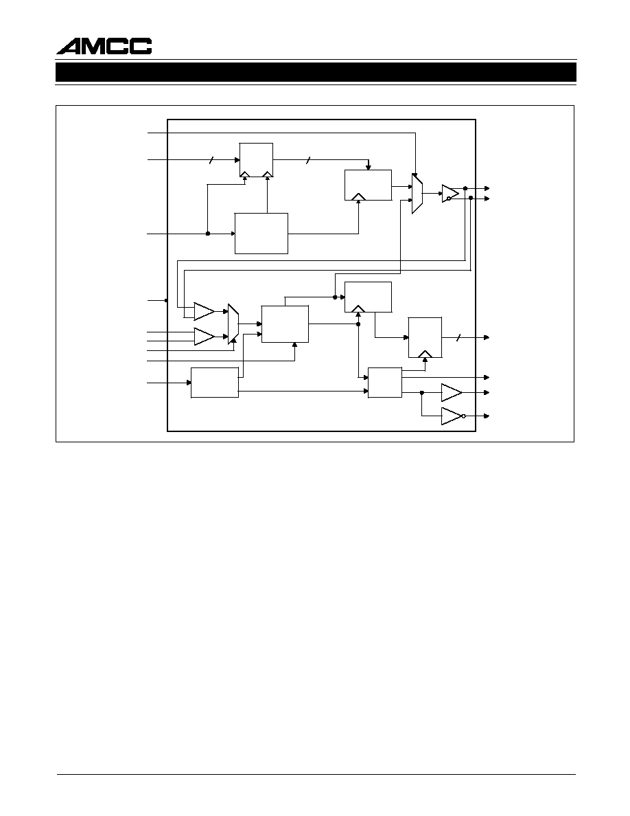
Figure 2. Functional Block Diagram
Fifo
(4x10)
Shift
Register
10
10
PLL Clock
Multiplier w/
Lock Detct
F0 = F1 x 10
PLL Clock
Recovery
w/ Lock
Detect
Shift
Register
D
Control
Logic
Comma
Detect
Logic
D
Q
10
TX[0-9]
TBC
RXP
RXN
EWRAP
-LCK_REF
EN_CDET
RBC0
RBC1
COM_DET
RX[0-9]
TXN
TXP
RATEN
2:1
I
O
2:1
PBCSEL

3
S2075
FIBRE CHANNEL BIT STREAM MONITOR WITH REPEATER
May 15, 2000 / Revision A
S2075 OVERVIEW
The S2075 provides repeater serialization and
deserialization functions for block encoded data to
implement a Fibre Channel interface. The S2075
functional block diagram is depicted in Figure 2.
The device operates in two basic modes, controlled
by the PBCSEL input, as shown in Table 1. In moni-
tor mode, the parallel input is unused, the device
functions as a repeater with parallel output monitor
capability. In transceiver mode, the device functions
as a fibre channel transceiver. The sequence of op-
eration for each mode is as follows:
Monitor Mode
1.
Serial Input
2.
Clock and data recovery
3a. Serial output
3b. Serial-to-parallel conversion, frame detection,
and 10-bit parallel output.
e
t
y
B
a
t
a
D
]
9
:
0
[
X
R
r
o
]
9
:
0
[
X
T
0
1
2
3
4
5
6
7
8
9
B
0
1
/
B
8
n
o
it
a
t
n
e
s
e
r
p
e
R
c
it
e
b
a
h
p
l
A
a
b
c
d
e
i
f
g
h
j
Table 2. Data Mapping to 8B/10B
Alphabetic Representation
1
A.X. Widmer and P.A. Franaszek, "A Byte Oriented DC Bal-
anced (0,4) 8B/10B Transmission Code," IBM Research Report
RC 9391, May 1982.
Table 1. Operating Modes
Transceiver Mode
Transmitter
1.
10-bit parallel input
2.
Parallel-to-serial conversion
3.
Serial output
Receiver
1.
Clock and data recoverery from serial input
2.
Serial-to-parallel conversion
3.
Frame detection
4.
10-bit parallel output
The 10-bit parallel data input to the S2075 should be
from a DC-balanced encoding scheme, such as the
8B/10B transmission code, in which information to be
transmitted is encoded 8 bits at a time into 10-bit trans-
mission characters
1
. For reference, Table 2 shows the
mapping of the parallel data to the 8B/10B codes.
Loop Back
Local loopback provides a capability for performing
off-line testing. This is useful for ensuring the integ-
rity of the serial channel before enabling the trans-
mission medium. It also allows for system
diagnostics.
Repeater
1. Fully differential for minimum deterministic jitter
accumulation (10 ps nominal).
2. High speed LVPECL I/O.
L
E
S
C
B
P
E
D
O
M
1
r
e
v
i
e
c
s
n
a
r
T
0
r
o
t
i
n
o
M

4
S2075
FIBRE CHANNEL BIT STREAM MONITOR WITH REPEATER
May 15, 2000 / Revision A
TRANSMITTER DESCRIPTION
The S2075 accepts 10-bit parallel input data and se-
rializes it for transmission over fiber optic or coaxial
cable media. The chip is fully compatible with the
ANSI X3T11 Fibre Channel standard, and supports
the Fibre Channel data rate of 1062 Mbps. The
S2075 uses a PLL to generate the serial rate trans-
mit clock. The transmitter runs at 10 times the TBC
input clock, and operates in either full rate or half
rate mode. At the full VCO rate the transmitter runs
at 1.062 GHz, while in half rate mode it operates at
531 MHz.
Parallel-to-Serial Conversion
The parallel-to-serial converter takes in 10-bit wide
data from the input latch and converts it to a serial
data stream. Parallel data is latched into the trans-
mitter on the positive going edge of TBC. The data is
then clocked into the serial output shift register. The
shift register is clocked by the internally generated
bit clock which is 10x the TBC input frequency. TX[0]
is transmitted first.
Transmit Byte Clock (TBC)
The Transmit Byte Clock input (TBC) must be sup-
plied from a clock source with 100 ppm tolerance to
assure that the transmitted data meets the Fibre
Channel frequency limits. The internal serial clock is
frequency locked to TBC (106.2 MHz).
TBC may be 53.1 MHz or 106.2 MHz, determined by
the state of the RATEN input. Operating rates are
shown in Table 3.
Transmit Latency
The average transmit latency is 4 byte times.
N
E
T
A
R
t
u
p
n
I
l
e
l
l
a
r
a
P
)
s
p
b
M
(
e
t
a
R
)
s
p
b
M
(
e
t
a
R
)
s
p
b
M
(
e
t
a
R
)
s
p
b
M
(
e
t
a
R
)
s
p
b
M
(
e
t
a
R
y
c
n
e
u
q
e
r
F
C
B
T
)
z
H
M
(
)
z
H
M
(
)
z
H
M
(
)
z
H
M
(
)
z
H
M
(
t
u
p
t
u
O
l
a
i
r
e
S
)
s
p
b
G
(
e
t
a
R
)
s
p
b
G
(
e
t
a
R
)
s
p
b
G
(
e
t
a
R
)
s
p
b
G
(
e
t
a
R
)
s
p
b
G
(
e
t
a
R
0
2
.
6
0
1
2
.
6
0
1
2
6
0
.
1
1
1
.
3
5
1
.
3
5
1
3
5
.
0
Table 3. Operating Rates
REPEATER DESCRIPTION
The S2075 provides serial input/output with a Clock
Recovery Unit (CRU) and a parallel output for moni-
toring of the serial bit stream. The S2075 retimes
incoming serial data, detects whether a valid charac-
ter is present, and outputs both a low jitter serial
data stream, and a 10-bit parallel data stream for
monitoring of the serial data. The S2075 complies
with the minimum jitter tolerance requirements pro-
posed by the Fibre Channel Jitter Working Group.
Jitter Performance
Jitter tolerance is defined as the amplitude of jitter
that causes the clock recovery PLL to violate the
BER specifications. This is specified as Frequency
Dependent, Random, and Deterministic jitter toler-
ance. Frequency Dependent jitter tolerance is de-
fined as the peak-to-peak amplitude of sinusoidal
jitter applied at the input. Figure 3 shows the Fre-
quency Dependent Jitter tolerance mask. Random
jitter tolerance is the amount of jitter with a Gaussian
distribution (noise) that the clock recovery PLL must
tolerate. Deterministic jitter tolerance is the amount
of jitter that is due to non-Gaussian events that the
clock recovery PLL must tolerate.
Figure 3. Frequency Dependent Jitter
Tolerance Mask
f
c
/25,000
(42.5 KHz)
Cut-off Freq A
f
c
/1,667
(637 KHz)
Cut-off Freq B
TIME (Unit Interval - UI)
1.5
Frequency (Hz)
(KHz) = Cut-off Freq @ 1,0625 Gbps

5
S2075
FIBRE CHANNEL BIT STREAM MONITOR WITH REPEATER
May 15, 2000 / Revision A
RECEIVER DESCRIPTION
Whenever a signal is present, the receiver attempts
to recover the serial clock from the received data
stream. The S2075 searches the serial bit stream for
the occurrence of a positive polarity comma sync
pattern (0011111xxx positive running disparity) to
perform word synchronization. Once synchronization
on both bit and word boundaries is achieved, the
receiver provides the decoded data on its parallel
outputs.
Clock Recovery Function
Clock recovery is performed on the input data
stream. A simple state machine in the clock recovery
macro decides whether to acquire lock from the se-
rial data input or from the reference clock. The deci-
sion is based upon the frequency and run length of
the input serial data.
The lock to reference frequency criteria ensure that
the S2075 will respond to variations in the serial data
input frequency (as compared to the reference fre-
quency). The new lock state is dependent upon the
current lock state, as shown in Table 4. The run-
length criteria ensure that the S2075 will respond ap-
propriately and quickly to a loss of signal. The run-
length checker flags a condition of consecutive ones
or zeros across 12 parallel words. Thus, 119 or less
consecutive ones or zeros does not cause signal loss,
129 or more causes signal loss, and 120 ≠ 128 may
or may not, depending on how the data aligns across
byte boundaries. If both the off-frequency detect test
and the run-length test is satisfied, the CRU will at-
tempt to lock to the incoming data.
In any transfer of PLL control between the serial
data and the reference clock, the RBC0 and RBC1
remain phase continuous and glitch free, assuring
the integrity of downstream clocking.
Reference Clock Input
The reference clock must be provided from a low
jitter clock source. The frequency of the received
data stream must be within 400 ppm of the reference
clock to ensure reliable locking of the receiver PLL.
A single reference clock is provided to both the
transmit and receive PLLs.
Data Output
The S2075 provides either framed or unframed par-
allel output data, determined by the state of
EN_CDET. With EN_CDET held ACTIVE, the S2075
will detect and align to the 8B/10B comma codeword
anywhere in the data stream. When EN_CDET is
INACTIVE, no attempt is made to synchronize on
any particular incoming character. The S2075 will
achieve bit synchronization within 250 bit times and
begin to deliver unframed parallel output data words
whenever it has received full transmission words.
Upon change of state of the EN_CDET input, the
COM_DET output response will be delayed by a
maximum of 3 byte times.
k
c
o
L
t
n
e
r
r
u
C
e
t
a
t
S
e
t
a
t
S
e
t
a
t
S
e
t
a
t
S
e
t
a
t
S
y
c
n
e
u
q
e
r
F
L
L
P
)
C
B
T
.
s
v
(
)
C
B
T
.
s
v
(
)
C
B
T
.
s
v
(
)
C
B
T
.
s
v
(
)
C
B
T
.
s
v
(
e
t
a
t
S
k
c
o
L
w
e
N
d
e
k
c
o
L
m
p
p
8
8
4
<
d
e
k
c
o
L
m
p
p
2
3
7
o
t
8
8
4
d
e
n
i
m
r
e
t
e
d
n
U
m
p
p
2
3
7
>
d
e
k
c
o
l
n
U
d
e
k
c
o
l
n
U
m
p
p
4
4
2
<
d
e
k
c
o
L
m
p
p
6
6
3
o
t
4
4
2
d
e
n
i
m
r
e
t
e
d
n
U
m
p
p
6
6
3
>
d
e
k
c
o
l
n
U
Table 4. Lock to Reference Frequency Criteria