 | –≠–ª–µ–∫—Ç—Ä–æ–Ω–Ω—ã–π –∫–æ–º–ø–æ–Ω–µ–Ω—Ç: S2076 | –°–∫–∞—á–∞—Ç—å:  PDF PDF  ZIP ZIP |

1
S2076
QUAD FIBRE CHANNEL TRANSCEIVER
May 19, 2000 / Revision A
S2076
Æ
QUAD FIBRE CHANNEL TRANSCEIVER
DEVICE
SPECIFICATION
FEATURES
∑ Functionally compliant with ANSI X3T11 Fibre
Channel physical and transmission protocol
standards.
∑ 1062 MHz (Fibre Channel) operating rate
- 1/2 Rate Operation
∑ Quad Transmitter incorporating phase-locked
loop (PLL) clock synthesis from low speed
reference
∑ Quad Receiver PLL provides clock and data
recovery
∑ Internally series terminated TTL outputs
∑ Low-jitter serial PECL interface
∑ Local Loopback
∑ Interfaces with coax, twinax, or fiber optics
∑ Single +3.3V supply, 2.3 W Power dissipation
∑ Compact 23mm x 23mm 208 TBGA package
APPLICATIONS
High-speed data communications
∑ Switched networks
∑ Data broadcast environments
∑ Fibre Channel Switches
GENERAL DESCRIPTION
The S2076 quad transmitter and receiver chip is de-
signed to provide four channels of high-speed serial
data transmission over fiber optic or copper interfaces
conforming to the requirements of the ANSI X3T11
Fibre Channel specification. The chip runs at 1062.5
Mbps serial data rate with an associated 10-bit paral-
lel data word. The chip provides four separate trans-
ceivers which can be operated individually at slightly
different frequencies.
Each bi-directional channel provides parallel to serial
and serial to parallel conversion, clock generation
and recovery, and framing. The on-chip transmit PLL
synthesizes the high-speed clock from a low-speed
reference. The on-chip quad receive PLL is used for
clock recovery and data re-timing on the four inde-
pendent data inputs. The transmitter and receiver
each support differential PECL-compatible I/O for
copper or fiber optic component interfaces and pro-
vide excellent signal integrity. Local loopback mode
allows for system diagnostics. The chip requires a
3.3V power supply and dissipates approximately 2.3
watts.
Figure 1 shows the use of the S2064 and S2076 in a
Fibre Channel application. Figure 2 summarizes the
input/output signals of the device. Figures 3 and 4
show the transmit and receive block diagrams, re-
spectively.
Figure 1. Typical Quad Fibre Channel Application
MAC
(ASIC)
S2064
QUAD
FIBRE
CHANNEL
INTERFACE
MAC
(ASIC)
MAC
(ASIC)
MAC
(ASIC)
TO SERIAL BACKPLANE
S2076
FC INTERFACE
SERIAL BP DRIVER

2
S2076
QUAD FIBRE CHANNEL TRANSCEIVER
May 19, 2000 / Revision A
Figure 2. S2076 Input/Output Diagram
REFCLK
TMODE
RATE
RESET
TCLKO
TXAP/N
TXBP/N
TXCP/N
TXDP/N
RXAP/N
RXBP/N
RXCP/N
RXDP/N
DINA[0:9]
10
DINB[0:9]
10
DINC[0:9]
10
DIND[0:9]
10
TBCA
TBCB
TBCC
TBCD
10
RBC1/0A
10
RBC1/0B
10
RBC1/0C
10
RBC1/0D
DOUTA[0:9]
DOUTB[0:9]
DOUTC[0:9]
DOUTD[0:9]
TESTMODE
CLKSEL
COM_DETA
COM_DETB
COM_DETC
COM_DETD
LPEN
CMODE
S2076
3
S2076
QUAD FIBRE CHANNEL TRANSCEIVER
May 19, 2000 / Revision A
Figure 3. Transmitter Block Diagram
TMODE
10
DINA[0:9]
10
Shift
Reg
10
DINB[0:9]
10
Shift
Reg
TBCB
10
DINC[0:9]
10
Shift
Reg
TBCC
10
DIND[0:9]
10
Shift
Reg
TBCD
DIN PLL
10x/20x
REFCLK
CLKSEL
MUX
RATE
REFCLK
TCLKO
FIFO
(input)
FIFO
(input)
FIFO
(input)
FIFO
(input)
TBCA
0 1
0 1
0 1
0 1
TXAP
TXAN
TXABP
TXBP
TXBN
TXBBP
TXCP
TXCN
TXCBP
TXDP
TXDN
TXDBP

4
S2076
QUAD FIBRE CHANNEL TRANSCEIVER
May 19, 2000 / Revision A
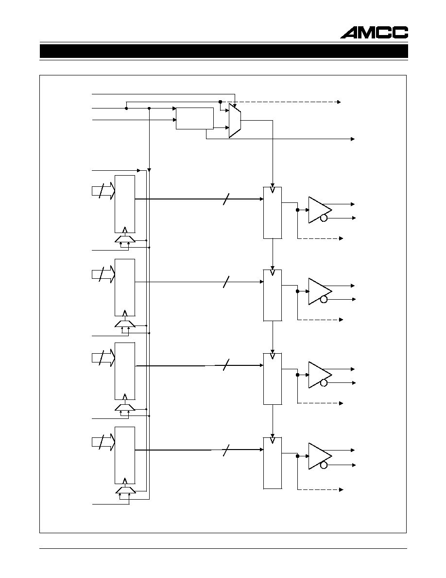
Figure 4. Receiver Block Diagram
DOUT CRU
Serial-
Parallel
DOUT CRU
Serial-
Parallel
DOUTA[0:9]
RXAP
RXAN
RXBP
RXBN
DOUTB[0:9]
Q
FIFO
(output)
DOUT CRU
Serial-
Parallel
DOUTD[0:9]
RXDP
RXDN
LPEN
DOUT CRU
Serial-
Parallel
DOUTC[0:9]
RXCP
RXCN
TXDBP
TXCBP
TXBBP
TXABP
REFCLK
10
10
10
10
10
RBC1/0A
2
RBC1/0B
2
RBC1/0C
2
RBC1/0D
CMODE
FIFO
(output)
FIFO
(output)
FIFO
(output)
10
10
10
COM_DETA
COM_DETB
COM_DETC
COM_DETD
2
5
S2076
QUAD FIBRE CHANNEL TRANSCEIVER
May 19, 2000 / Revision A
TRANSMITTER DESCRIPTION
The transmitter section of the S2076 contains a
single PLL which is used to generate the serial rate
transmit clock for all transmitters. Transmitter
functionalities are shown schematically in Figure 3.
Four channels are provided with a variety of options
regarding input clocking and loopback. The transmit-
ters operate at 1.062 GHz, 10 or 20 times the refer-
ence clock frequency.
Data Input
The S2076 has been designed to simplify the paral-
lel interface data transfer and provides flexibility in
the clocking of parallel data. Prior implementations
of this function have either forced the user to syn-
chronize transmit data to the reference clock or to
provide the output clock as a reference to the PLL,
resulting in increased jitter at the serial interface.
The S2076 incorporates a unique FIFO structure
which enables the user to provide a "clean" refer-
ence source for the PLL and to accept a separate
external clock which is used exclusively to reliably
clock data into the device.
The S2076 also provides a system clock output,
TCLKO, which is derived from the internal VCO. The
frequency of this output is constant at the parallel
word rate, 1/10 the serial data rate, regardless of
whether the reference is provided at 1/10 or 1/20 the
serial data rate. This clock can be used by upstream
circuitry as a system clock. See Table 2.
Data to be input to the S2076 should be coded to
insure transition density and DC balance. Data is
input to each channel of the S2076 as a 10 bit wide
word. An input FIFO and a clock input, TBCx, are
provided for each channel of the S2076. The device
can operate in two different modes. The S2076 can
be configured to use either the TBCx (TBC MODE)
input or the REFCLK input (REFCLK MODE). Table
1 provides a summary of the input modes for the
S2076.
Operation in the TBC MODE makes it easier for us-
ers to meet the relatively narrow setup and hold time
window required by the parallel 10-bit interface. The
TBC signal is used to clock the data into an internal
holding register and the S2076 synchronizes its in-
ternal data flow to insure stable operation. REFCLK,
not TBCx, is used as the reference for the DIN PLL.
This insures minimum jitter on the high speed serial
data stream.
The TBC must be frequency locked to REFCLK, but
may have an arbitrary but fixed phase relationship.
Adjustment of internal timing of the S2076 is per-
formed during reset. Once synchronized, the S2076
can tolerate up to
±
3ns of phase drift between TBC
and REFCLK.
E
D
O
M
T
n
o
i
t
a
r
e
p
O
0
.
s
l
e
n
n
a
h
c
ll
a
r
o
f
d
e
s
u
K
L
C
F
E
R
.
e
d
o
M
K
L
C
F
E
R
1
ll
a
o
t
n
i
a
t
a
d
k
c
o
l
c
o
t
d
e
s
u
x
C
B
T
.
e
d
o
M
C
B
T
.
s
O
F
I
F
E
T
A
R
L
E
S
K
L
C
K
L
C
F
E
R
y
c
n
e
u
q
e
r
F
t
u
p
t
u
O
l
a
i
r
e
S
e
t
a
R
0
K
L
C
T
q
e
r
F
0
0
0
1
/
R
D
S
s
p
b
M
5
.
2
6
0
1
0
1
/
R
D
S
0
1
0
2
/
R
D
S
s
p
b
M
5
.
2
6
0
1
0
1
/
R
D
S
1
0
0
1
/
R
D
S
s
p
b
M
5
2
.
1
3
5
0
1
/
R
D
S
1
1
0
2
/
R
D
S
s
p
b
M
5
2
.
1
3
5
0
1
/
R
D
S
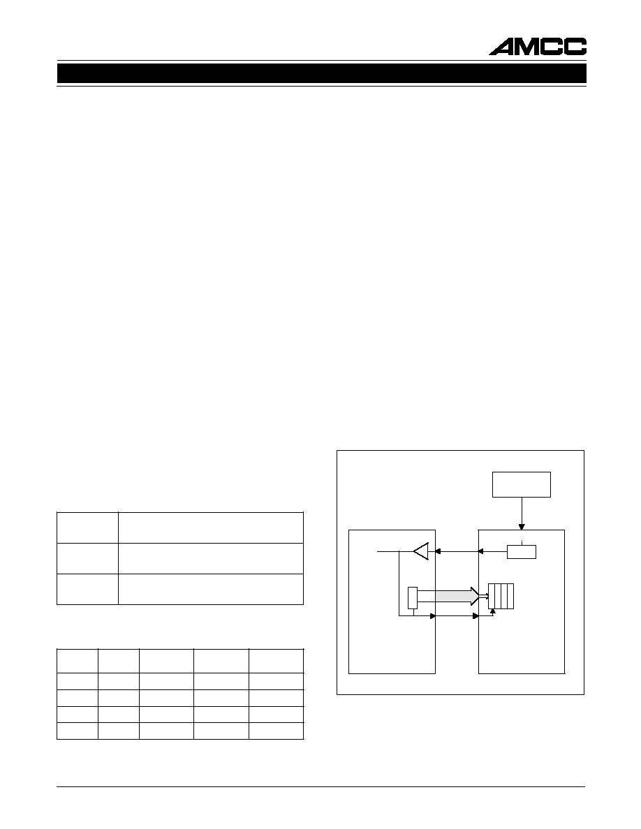
Table 1. Input Modes
Table 2. Operating Rates
REFCLK
S2076
106.25 MHz or 53.125 MHz
TBCx
DINx[0:9]
REF
OSCILLATOR
MAC
ASIC
TCLKO
PLL
Figure 5. DIN Clocking with TBC
Note that internal synchronization of FIFOs is performed upon
de-assertion of RESET.
Note: SDR = Serial Data Rate.