 | –≠–ª–µ–∫—Ç—Ä–æ–Ω–Ω—ã–π –∫–æ–º–ø–æ–Ω–µ–Ω—Ç: S2078 | –°–∫–∞—á–∞—Ç—å:  PDF PDF  ZIP ZIP |

1
S2078
DUAL FIBRE CHANNEL TRANSCEIVER
June 20, 2000 / Revision B
S2078
Æ
DUAL FIBRE CHANNEL TRANSCEIVER
DEVICE
SPECIFICATION
FEATURES
∑ Functionally compliant with ANSI X3T11 Fibre
Channel physical and transmission protocol
standards
∑ 1062 MHz (Fibre Channel) operating rate
- Half rate operation
∑ Dual Transmitter incorporating phase-locked
loop (PLL) clock synthesis from low speed
reference
∑ Dual Receiver PLL provides clock and data
recovery
∑ Internally Series terminated TTL outputs
∑ Low-jitter serial PECL interface
∑ Local Loopback
∑ Interfaces with coax, twinax, or fiber optics
∑ Single +3.3V supply, 1.33 W power dissipation
∑ Compact 21mm x 21mm 156 TBGA package
APPLICATIONS
High-speed data communications
∑ Switched networks
∑ Data broadcast environments
∑ Fibre Channel Switches
GENERAL DESCRIPTION
The S2078 dual transmitter and receiver chip is de-
signed to provide two channels of high-speed serial
data transmission over fiber optic or copper interfaces
conforming to the requirements of the ANSI X3T11
Fibre Channel specification. The chip runs at 1062.5
Mbps serial data rate with an associated 10-bit paral-
lel data word. The chip provides two separate receive
PLLs which can be operated asyncronously.
Each bi-directional channel provides parallel-to-se-
rial and serial-to-parallel conversion, clock genera-
tion and recovery, and framing. The on-chip transmit
PLL synthesizes the high-speed clock from a low-
speed reference. The on-chip dual receive PLL is
used for clock recovery and data re-timing on the
two independent data inputs. The transmitter and re-
ceiver each support differential PECL-compatible I/O
for copper or fiber optic component interfaces and
provide excellent signal integrity. Local loopback
mode allows for system diagnostics. The chip re-
quires a 3.3V power supply and dissipates 1.33
watts.
Figure 1 shows the use of the S2062 and S2078 in a
Fibre Channel application. Figure 2 summarizes the
input/output signals of the device. Figures 3 and 4
show the transmit and receive block diagrams, re-
spectively.
Figure 1. Typical Dual Fibre Channel Application
MAC
(ASIC)
S2062
DUAL
FIBRE
CHANNEL
INTERFACE
MAC
(ASIC)
TO SERIAL
BACKPLANE
S2078
FC INTERFACE
SERIAL BP DRIVER
2
S2078
DUAL FIBRE CHANNEL TRANSCEIVER
June 20, 2000 / Revision B
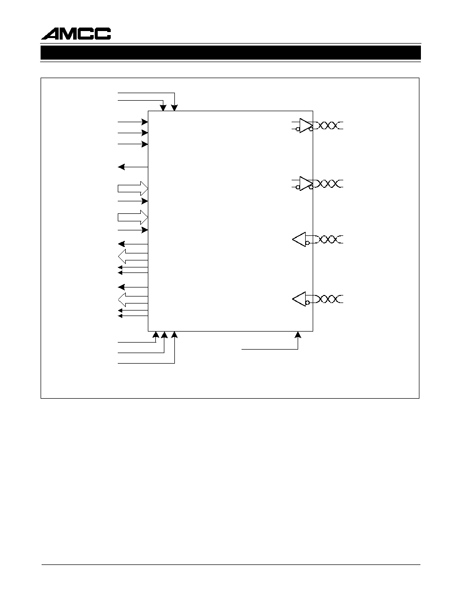
Figure 2. S2078 Input/Output Diagram
REFCLK
RATE
RESET
TCLKO
TXAP/N
TXBP/N
RXAP/N
RXBP/N
DINA[0:9]
10
DINB[0:9]
10
TBCA
TBCB
10
RBC1/0A
10
RBC1/0B
DOUTA[0:9]
DOUTB[0:9]
CLKSEL
COM_DETA
COM_DETB
LPEN
CMODE
TMODE
TESTMODE1
TESTMODE

3
S2078
DUAL FIBRE CHANNEL TRANSCEIVER
June 20, 2000 / Revision B
Figure 3. Transmitter Block Diagram
10
DINA[0:9]
10
Shift
Reg
10
DINB[0:9]
10
Shift
Reg
TBCB
DIN PLL
10x/20x
REFCLK
CLKSEL
MUX
RATE
REFCLK
TCLKO
FIFO
(input)
FIFO
(input)
TBCA
TXAP
TXAN
TXABP
TXBP
TXBN
TXBBP
0 1
TMODE
0 1

4
S2078
DUAL FIBRE CHANNEL TRANSCEIVER
June 20, 2000 / Revision B
Figure 4. Receiver Block Diagram
DOUT CRU
Serial-
Parallel
DOUT CRU
Serial-
Parallel
DOUTA[0:9]
RXAP
RXAN
RXBP
RXBN
DOUTB[0:9]
Q
FIFO
(output)
LPEN
TXBBP
TXABP
REFCLK
10
10
RBC1/0A
2
RBC1/0B
2
CMODE
RATE
FIFO
(output)
10
10
COM_DETA
COM_DETB

5
S2078
DUAL FIBRE CHANNEL TRANSCEIVER
June 20, 2000 / Revision B
TRANSMITTER DESCRIPTION
The transmitter section of the S2078 contains a
single PLL which is used to generate the serial rate
transmit clock for all transmitters. Transmitter
functionalities shown schematically in Figure 3. Two
channels are provided with a variety of options re-
garding input clocking and loopback. The transmit-
ters operate at 1.062 GHz, 10 or 20 times the
reference clock frequency.
Data Input
The S2078 has been designed to simplify the paral-
lel interface data transfer and provides flexibility in
the clocking of parallel data. Prior implementations
of this function have either forced the user to syn-
chronize transmit data to the reference clock or to
provide the output clock as a reference to the PLL,
resulting in increased jitter at the serial interface.
The S2078 incorporates a unique FIFO structure
which enables the user to provide a "clean" refer-
ence source for the PLL and to accept a separate
external clock which is used exclusively to reliably
clock data into the device.
The S2078 also provides a system clock output,
TCLKO, which is derived from the internal VCO. The
frequency of this output is constant at the parallel
word rate, 1/10 the serial data rate, regardless of
whether the reference is provided at 1/10 or 1/20 the
serial data rate. This clock can be used by upstream
circuitry as a system clock. See Table 1.
Data to be input to the S2078 should be coded to
insure transition density and DC balance. Data is input
to each channel of the S2078 as a 10 bit wide word. An
input FIFO and a clock input, TBCx, are provided for
each channel of the S2078. The device can operate in
two different modes. The S2078 can be configured to
use either the TBCx (TBC MODE) input or the
REFCLK input (REFCLK MODE). Table 2 provides a
summary of the input modes for the S2078.
Operation in the TBC MODE makes it easier for us-
ers to meet the relatively narrow setup and hold time
window required by the 106.25 Mbps 10 bit inter-
face. The TBC signal is used to clock the data into
an internal holding register and the S2078 synchro-
nizes its internal data flow to ensure stable opera-
tion. REFCLK, not TBCx, is used as the reference
for the transmit PLL. This ensures minimum jitter on
the high speed serial data stream.
The TBC must be frequency locked to REFCLK, but
may have an arbitrary but fixed phase relationship. Ad-
justment of internal timing of the S2078 is performed
during reset. Once synchronized, the S2078 can tolerate
up to
±
3ns of phase drift between TBC and REFCLK.
Figure 5 demonstrates the flexibility afforded by the
S2078. A low jitter reference is provided directly to
the S2078 at either 1/10 or 1/20 the serial data rate.
This insures minimum jitter in the synthesized clock
used for serial data transmission. A system clock
output at the parallel word rate, TCLKO, is derived
from the PLL and provided to the upstream circuit as
a system clock. This clock can be buffered as re-
quired without concern about added delay. There is
no phase requirement placed upon TCLKO and the
TBCx clock, which is provided back to the S2078,
E
T
A
R
L
E
S
K
L
C
K
L
C
F
E
R
y
c
n
e
u
q
e
r
F
t
u
p
t
u
O
l
a
i
r
e
S
e
t
a
R
0
K
L
C
T
y
c
n
e
u
q
e
r
F
0
0
0
1
/
R
D
S
s
p
b
M
5
.
2
6
0
1
0
1
/
R
D
S
0
1
0
2
/
R
D
S
s
p
b
M
5
.
2
6
0
1
0
1
/
R
D
S
1
0
0
1
/
R
D
S
s
p
b
M
5
2
.
1
3
5
0
1
/
R
D
S
1
1
0
2
/
R
D
S
s
p
b
M
5
2
.
1
3
5
0
1
/
R
D
S
Table 1. Operating Rates
REFCLK
S2078
106.25 MHz or 53.125 MHz
TBCx
DINx[0:9]
REF
OSCILLATOR
MAC
ASIC
TCLKO
PLL
Figure 5. DIN Clocking with TBC
E
D
O
M
T
n
o
i
t
a
r
e
p
O
0
a
t
a
d
k
c
o
l
c
o
t
d
e
s
u
K
L
C
F
E
R
.
e
d
o
M
K
L
C
F
E
R
.
s
l
e
n
n
a
h
c
ll
a
r
o
f
s
O
F
I
F
o
t
n
i
1
s
O
F
I
F
o
t
n
i
a
t
a
d
k
c
o
l
c
o
t
d
e
s
u
x
C
B
T
.
e
d
o
M
C
B
T
.
s
l
e
n
n
a
h
c
ll
a
r
o
f
Table 2. Input Modes
Note that internal synchronization of FIFOs is performed upon
de-assertion of RESET.
Note: SDR = Serial Data Rate.

6
S2078
DUAL FIBRE CHANNEL TRANSCEIVER
June 20, 2000 / Revision B
other than that they remain within
±
3ns of the phase
relationship established at reset.
The S2078 also supports the traditional REFCLK
clocking found in many Fibre Channel applications
and is illustrated in Figure 6.
Half Rate Operation
The S2078 supports full and half rate operation for
all modes of operation. When RATE is LOW, the
S2078 serial data rate equals the VCO frequency.
When RATE is HIGH, the VCO is divided by 2 before
being provided to the chip. Thus the S2078 can sup-
port Fibre Channel and serial backplane functions at
both full and 1/2 the VCO rate.
Parallel to Serial Conversion
The 10-bit parallel data handled by the S2078 device
should be from a DC-balanced encoding scheme,
such as the 8B/10B transmission code, in which in-
formation to be transmitted is encoded, 8 bits at a
time, into a 10-bit transmission character and must
be compliant with ANSI X3.230 FC-PH (Fibre Chan-
nel Physical and Signaling Interface).
The 8B/10B transmission code includes serial encod-
ing and decoding rules, special characters, and error
control. Information is encoded, 8 bits at a time, into a
10 bit transmission character. The characters defined
by this code ensure that short run lengths and enough
transitions are present in the serial bit stream to make
clock recovery possible at the receiver. The encoding
also greatly increases the likelihood of detecting any
single or multiple errors that might occur during the
transmission and reception of data
1
.
Table 3 identifies the mapping of the 8B/10B charac-
ters to the data inputs of the S2078. The S2078 will
serialize the parallel data for each channel and will
transmit bit "a" or DIN[0] first.
Frequency Synthesizer (PLL)
The S2078 synthesizes a serial transmit clock from
the reference signal provided. The S2078 will obtain
phase and frequency lock within 2500 bit times after
the start of receiving reference clock inputs. Reliable
locking of the transmit PLL is assured, but a lock-
detect output is NOT provided.
Reference Clock Input
The reference clock input must be supplied with a low-
jitter clock source. All reference clocks in a system
must be within 200 ppm of each other to ensure that
the clock recovery units can lock to the serial data.
The frequency of the reference clock must be either
1/10 the serial data rate, CLKSEL = 0, or 1/20 the
serial data rate, CLKSEL = 1. Note that in both
cases, the frequency of the parallel word rate output,
TCLKO, is constant at 1/10 the serial data rate.
Serial Data Outputs
The S2078 provides LVPECL level serial outputs.
Each high speed output should be provided with a
resistor to VSS (Gnd) near the device. A value of
4.5K
provides optimal performance with minimum
impact on power dissipation. The resistance may be
as low as 450
, but will dissipate additional power
with no substantive performance improvement.
Transmit FIFO Initialization
The transmit FIFO must be initialized after stable de-
livery of data and TBC to the parallel interface, and
before entering the normal operational state of the
circuit. FIFO initialization is performed upon the de-
assertion of the RESET signal. The TCLKO output will
operate normally even when RESET is asserted and
is available for use as an upstream clock source.
e
t
y
B
a
t
a
D
]
9
:
0
[
T
U
O
D
r
o
]
9
:
0
[
N
I
D
0
1
2
3
4
5
6
7
8
9
.
r
p
e
r
.
h
p
l
a
B
0
1
/
B
8
a
b
c
d
e
i
f
g
h
j
Table 3. Data to 8B/10B Alphabetic Representation
1. A.X. Widner and P.A. Franaszek, "A Byte-Oriented DC Bal-
anced (0,4) 8B/10B Transmission Code," IBM Research Report
RC9391, May 1982.
REFCLK
S2078
TBCx
DINx[0:9]
REF
OSCILLATOR
MAC
ASIC
TCLKO
PLL
106.25 MHz
Figure 6. FC DIN Clocking with REFCLK

7
S2078
DUAL FIBRE CHANNEL TRANSCEIVER
June 20, 2000 / Revision B
RECEIVER DESCRIPTION
Each receiver channel is designed to implement the
ANSI X3T11 Fibre Channel specification. A block
diagram showing the basic function is provided in
Figure 4.
Whenever a signal is present, the receiver attempts
to recover the serial clock from the received data
stream. After acquiring bit synchronization, the
S2078 searches the serial bit stream for the occur-
rence of a K28.5 character on which to perform word
synchronization. Once synchronization on both bit
and word boundaries is achieved, the receiver pro-
vides the word-aligned data on its parallel outputs.
Data Input
A differential input receiver is provided for each
channel of the S2078. Each channel has a loopback
mode in which the serial data from the transmitter
replaces external serial data. The loopback function
for the two channels is controlled by the loopback
enable signal, LPEN.
The high speed serial inputs to the S2078 are inter-
nally biased to VDD≠1.3V. This facilities AC-coupling
of the differential inputs and termination with a single
differential termination. For applications in which
long periods of no data present may occur, a small
positive bias, relative to the inverting input, should
be created on the non-inverting input by connecting
a 10K
resistor to VDD. This will prevent oscillation
of the input stage during loss of input.
Clock Recovery Function
Clock recovery is provided for each channel of the
S2078. The receiver PLL has been optimized for the
needs of Fibre Channel systems. A simple state ma-
chine in the clock recovery macro decides whether to
acquire lock from the serial data input or from the
reference clock. The decision is based upon the fre-
quency and run length of the serial data inputs.
The run-length requirements insure that the S2078
will respond appropriately and quickly to a loss of
signal. The run-length checker looks for a minimum
of 120 consecutive ones or zeros. The checking is
done in parallel, thus 12 parallel words are exam-
ined.
An off-frequency detection circuit in the S2078 moni-
tors the receiver VCO frequency to insure that the
input signal is at a valid data rate. The data stream
must be within 200 ppm of the appropriate rate for
reliable locking of the CRU to the data stream.
If both the off-frequency test and the run-length test
are satisfied, the CRU will attempt to lock to the
incoming data. Note that if the run length test is sat-
isfied due to noise on the inputs, and no signal is
present, the receiver VCO will maintain frequency
accuracy to within 100 ppm of the target rate as
determined by the REFCLK.
In any transfer of PLL control from the serial data to
the reference clock, the RBC1/0x outputs remain
phase continuous and glitch free, assuring the integ-
rity of downstream clocking.
If at any time, the frequency or run length checks are
violated, the state machine forces the VCO to lock to
the reference clock. This is required to guarantee
that the VCO maintains the correct frequency in the
absence of data.
Reference Clock Input
The reference clock must be provided from a low
jitter clock source. The frequency of the received
data stream (divided by 10 or 20) must be within 200
ppm of the reference clock to insure reliable locking
of the receiver PLL. A single reference clock is pro-
vided to both the transmitter and the receiver of the
S2078.

8
S2078
DUAL FIBRE CHANNEL TRANSCEIVER
June 20, 2000 / Revision B
Serial-to-Parallel Conversion
Once bit synchronization has been attained by the
S2078 CRU, the S2078 must synchronize to the 10
bit word boundary. Word synchronization in the
S2078 is accomplished by detecting and aligning to
the 8B/10B K28.5 codeword. The S2078 will detect
and byte-align to either polarity of the K28.5. Each
channel of the S2078 will detect and align to a K28.5
anywhere in the data stream. The presence of a
K28.5 is indicated for each channel by the assertion
of the COM_DETx (Comma Detect) signal.
Data Output
Data is output on the DOUTx[0:9] outputs. The
COM_DETx signal is used to indicate the reception
of a valid K28.5 character and is driven concurrent
with the K28.5 character on the DOUTx[0:9] outputs.
The S2078 TTL outputs are optimized to drive 65
line impedences. Internal source matching provides
good performance on unterminated lines of reason-
able length.
Parallel Output Clock Rate
Two output clock modes are supported. When
CMODE is HIGH, a complementary TTL clock at the
data rate is provided on the RBC1/0x outputs. Data
should be clocked on the rising edge of RBC1x.
When CMODE is LOW, the S2078 outputs a
complementary TTL clock at 1/2 the data rate in
compliance with the the Fibre Channel 10 Bit Inter-
face Specification. Data should be latched on the
rising edge of RBC1x and the rising edge of RBC0x.
If consecutive K28.5 characters are received, the
S2078 RBC1/0x clock operates without glitches or
loss of cycles.
e
d
o
M
E
D
O
M
C
.
q
e
r
F
x
0
/
1
C
B
R
e
d
o
M
k
c
o
l
C
f
l
a
H
0
z
H
M
5
2
1
.
3
5
e
d
o
M
k
c
o
l
C
ll
u
F
1
z
H
M
5
.
2
6
0
1
Table 4. Output Clock Modes

9
S2078
DUAL FIBRE CHANNEL TRANSCEIVER
June 20, 2000 / Revision B
e
m
a
N
n
i
P
l
e
v
e
L
O
/
I
#
n
i
P
n
o
i
t
p
i
r
c
s
e
D
P
A
X
T
N
A
X
T
.
f
f
i
D
L
C
E
P
V
L
O
6
1
D
5
1
E
.
A
l
e
n
n
a
h
C
r
o
f
s
t
u
p
t
u
o
l
a
i
r
e
s
d
e
e
p
s
h
g
i
H
P
B
X
T
N
B
X
T
.
f
f
i
D
L
C
E
P
V
L
O
5
1
G
6
1
G
.
B
l
e
n
n
a
h
C
r
o
f
s
t
u
p
t
u
o
l
a
i
r
e
s
d
e
e
p
s
h
g
i
H
O
K
L
C
T
L
T
T
O
4
1
K
r
o
f
d
e
d
i
v
o
r
p
s
i
k
c
o
l
c
s
i
h
T
.
e
t
a
r
a
t
a
d
l
e
ll
a
r
a
p
e
h
t
t
a
k
c
o
l
C
t
u
p
t
u
O
L
T
T
.
y
r
t
i
u
c
r
i
c
m
a
e
r
t
s
-
p
u
y
b
e
s
u
Table 6. Transmitter Output Signals Assignment and Descriptions
e
m
a
N
n
i
P
l
e
v
e
L
O
/
I
#
n
i
P
n
o
i
t
p
i
r
c
s
e
D
9
A
N
I
D
8
A
N
I
D
7
A
N
I
D
6
A
N
I
D
5
A
N
I
D
4
A
N
I
D
3
A
N
I
D
2
A
N
I
D
1
A
N
I
D
0
A
N
I
D
L
T
T
I
5
1
T
3
1
R
2
1
P
4
1
T
2
1
R
1
1
P
3
1
T
1
1
R
2
1
T
0
1
P
d
e
k
c
o
l
c
s
i
s
u
b
s
i
h
t
n
o
a
t
a
d
l
e
ll
a
r
a
P
.
A
l
e
n
n
a
h
C
r
o
f
a
t
a
D
t
i
m
s
n
a
r
T
.
K
L
C
F
E
R
r
o
A
C
B
T
f
o
e
g
d
e
g
n
i
s
i
r
e
h
t
n
o
n
i
A
C
B
T
L
T
T
I
0
1
R
d
e
s
u
s
i
l
a
n
g
i
s
s
i
h
t
,
h
g
i
H
s
i
E
D
O
M
T
n
e
h
W
.
A
k
c
o
l
C
e
t
y
B
t
i
m
s
n
a
r
T
,
w
o
L
s
i
E
D
O
M
T
n
e
h
W
.
8
7
0
2
S
e
h
t
o
t
n
i
]
9
:
0
[
A
N
I
D
n
o
a
t
a
D
k
c
o
l
c
o
t
.
d
e
r
o
n
g
i
s
i
A
C
B
T
9
B
N
I
D
8
B
N
I
D
7
B
N
I
D
6
B
N
I
D
5
B
N
I
D
4
B
N
I
D
3
B
N
I
D
2
B
N
I
D
1
B
N
I
D
0
B
N
I
D
L
T
T
I
5
1
L
4
1
L
6
1
M
5
1
M
4
1
M
6
1
N
5
1
N
4
1
N
6
1
P
5
1
P
n
i
d
e
k
c
o
l
c
s
i
s
u
b
s
i
h
t
n
o
a
t
a
d
l
e
ll
a
r
a
P
.
B
l
e
n
n
a
h
C
r
o
f
a
t
a
D
t
i
m
s
n
a
r
T
B
C
B
T
f
o
e
g
d
e
g
n
i
s
i
r
e
h
t
n
o
.
K
L
C
F
E
R
r
o
B
C
B
T
L
T
T
I
6
1
R
d
e
s
u
s
i
l
a
n
g
i
s
s
i
h
t
,
h
g
i
H
s
i
E
D
O
M
T
n
e
h
W
.
B
k
c
o
l
C
e
t
y
B
t
i
m
s
n
a
r
T
,
w
o
L
s
i
E
D
O
M
T
n
e
h
W
.
8
7
0
2
S
e
h
t
o
t
n
i
]
9
:
0
[
B
N
I
D
n
o
a
t
a
D
k
c
o
l
c
o
t
.
d
e
r
o
n
g
i
s
i
B
C
B
T
Table 5. Transmitter Input Signals Assignment and Descriptions
Note: All TTL inputs except REFCLK have internal pull-up networks.

10
S2078
DUAL FIBRE CHANNEL TRANSCEIVER
June 20, 2000 / Revision B
Table 8. Receiver Input Signals Assignment and Descriptions
e
m
a
N
n
i
P
l
e
v
e
L
O
/
I
#
n
i
P
n
o
i
t
p
i
r
c
s
e
D
P
A
X
R
N
A
X
R
.
f
f
i
D
L
C
E
P
V
L
I
5
B
4
A
e
h
t
s
i
P
A
X
R
.
A
l
e
n
n
a
h
c
r
o
f
s
t
u
p
n
i
e
l
b
i
t
a
p
m
o
c
L
C
E
P
V
L
l
a
i
t
n
e
r
e
f
f
i
D
D
D
V
o
t
d
e
s
a
i
b
y
ll
a
n
r
e
t
n
I
.
e
v
i
t
a
g
e
n
e
h
t
s
i
N
A
X
R
,
t
u
p
n
i
e
v
i
t
i
s
o
p
.
s
n
o
i
t
a
c
il
p
p
a
d
e
l
p
u
o
c
C
A
r
o
f
V
3
.
1
≠
P
B
X
R
N
B
X
R
.
f
f
i
D
L
C
E
P
V
L
I
0
1
B
1
1
A
e
h
t
s
i
P
B
X
R
.
B
l
e
n
n
a
h
c
r
o
f
s
t
u
p
n
i
e
l
b
i
t
a
p
m
o
c
L
C
E
P
V
L
l
a
i
t
n
e
r
e
f
f
i
D
D
D
V
o
t
d
e
s
a
i
b
y
ll
a
n
r
e
t
n
I
.
e
v
i
t
a
g
e
n
e
h
t
s
i
N
B
X
R
,
t
u
p
n
i
e
v
i
t
i
s
o
p
.
s
n
o
i
t
a
c
il
p
p
a
d
e
l
p
u
o
c
C
A
r
o
f
V
3
.
1
≠
Table 7. Receiver Output Signals Assignment and Descriptions
e
m
a
N
n
i
P
l
e
v
e
L
O
/
I
#
n
i
P
n
o
i
t
p
i
r
c
s
e
D
9
A
T
U
O
D
8
A
T
U
O
D
7
A
T
U
O
D
6
A
T
U
O
D
5
A
T
U
O
D
4
A
T
U
O
D
3
A
T
U
O
D
2
A
T
U
O
D
1
A
T
U
O
D
0
A
T
U
O
D
L
T
T
O
2
J
2
G
2
L
1
L
2
K
1
K
3
J
1
J
3
H
2
H
d
il
a
v
s
i
s
u
b
s
i
h
t
n
o
a
t
a
d
l
e
ll
a
r
a
P
.
s
t
u
p
t
u
O
a
t
a
D
r
e
v
i
e
c
e
R
A
l
e
n
n
a
h
C
e
h
t
n
o
d
il
a
v
d
n
a
e
d
o
m
k
c
o
l
c
ll
u
f
n
i
A
1
C
B
R
f
o
e
g
d
e
g
n
i
s
i
r
e
h
t
n
o
.
e
d
o
m
k
c
o
l
c
f
l
a
h
n
i
A
0
C
B
R
d
n
a
A
1
C
B
R
h
t
o
b
f
o
e
g
d
e
g
n
i
s
i
r
A
T
E
D
_
M
O
C
L
T
T
O
1
G
a
t
a
h
t
s
e
t
a
c
i
d
n
i
t
u
p
t
u
o
s
i
h
t
n
o
h
g
i
H
A
.
t
c
e
t
e
D
a
m
m
o
C
A
l
e
n
n
a
h
C
a
t
a
d
l
e
ll
a
r
a
p
e
h
t
n
o
t
n
e
s
e
r
p
s
i
d
n
a
d
e
t
c
e
t
e
d
n
e
e
b
s
a
h
5
.
8
2
K
d
il
a
v
.
]
9
:
0
[
A
T
U
O
D
s
t
u
p
t
u
o
A
1
C
B
R
A
0
C
B
R
L
T
T
O
1
M
3
L
d
n
a
]
9
:
0
[
A
T
U
O
D
,
a
t
a
d
e
v
i
e
c
e
r
l
e
l
l
a
r
a
P
.
s
k
c
o
l
C
e
t
y
B
e
v
i
e
c
e
R
ll
u
f
n
i
n
e
h
w
A
1
C
B
R
f
o
e
g
d
e
g
n
i
s
i
r
e
h
t
n
o
d
il
a
v
e
r
a
A
T
E
D
_
M
O
C
d
n
a
A
1
C
B
R
h
t
o
b
f
o
e
g
d
e
g
n
i
s
i
r
e
h
t
n
o
d
i
l
a
v
d
n
a
e
d
o
m
k
c
o
l
c
.
e
d
o
m
k
c
o
l
c
f
l
a
h
n
i
A
0
C
B
R
9
B
T
U
O
D
8
B
T
U
O
D
7
B
T
U
O
D
6
B
T
U
O
D
5
B
T
U
O
D
4
B
T
U
O
D
3
B
T
U
O
D
2
B
T
U
O
D
1
B
T
U
O
D
0
B
T
U
O
D
L
T
T
O
4
P
1
R
8
P
5
T
6
R
6
P
5
R
3
T
5
P
3
R
d
il
a
v
s
i
s
u
b
s
i
h
t
n
o
a
t
a
d
l
e
ll
a
r
a
P
.
s
t
u
p
t
u
O
a
t
a
D
r
e
v
i
e
c
e
R
B
l
e
n
n
a
h
C
g
n
i
s
i
r
n
o
d
il
a
v
d
n
a
e
d
o
m
k
c
o
l
c
ll
u
f
n
i
B
1
C
B
R
f
o
e
g
d
e
g
n
i
s
i
r
e
h
t
n
o
.
e
d
o
m
k
c
o
l
c
f
l
a
h
n
i
B
0
C
B
R
d
n
a
B
1
C
B
R
h
t
o
b
f
o
e
g
d
e
B
T
E
D
_
M
O
C
L
T
T
O
2
P
a
t
a
h
t
s
e
t
a
c
i
d
n
i
t
u
p
t
u
o
s
i
h
t
n
o
h
g
i
H
A
.
t
c
e
t
e
D
a
m
m
o
C
B
l
e
n
n
a
h
C
a
t
a
d
l
e
ll
a
r
a
p
e
h
t
n
o
t
n
e
s
e
r
p
s
i
d
n
a
d
e
t
c
e
t
e
d
n
e
e
b
s
a
h
5
.
8
2
K
d
il
a
v
.
]
9
:
0
[
B
T
U
O
D
s
t
u
p
t
u
o
B
1
C
B
R
B
0
C
B
R
L
T
T
O
7
R
7
P
d
n
a
]
9
:
0
[
B
T
U
O
D
,
a
t
a
d
e
v
i
e
c
e
r
l
e
l
l
a
r
a
P
.
s
k
c
o
l
C
e
t
y
B
e
v
i
e
c
e
R
ll
u
f
n
i
n
e
h
w
B
1
C
B
R
f
o
e
g
d
e
g
n
i
s
i
r
e
h
t
n
o
d
il
a
v
e
r
a
B
T
E
D
_
M
O
C
d
n
a
B
1
C
B
R
h
t
o
b
f
o
e
g
d
e
g
n
i
s
i
r
e
h
t
n
o
d
i
l
a
v
d
n
a
e
d
o
m
k
c
o
l
c
.
e
d
o
m
k
c
o
l
c
f
l
a
h
n
i
B
0
C
B
R

11
S2078
DUAL FIBRE CHANNEL TRANSCEIVER
June 20, 2000 / Revision B
Note: All TTL inputs except REFCLK have internal pull-up networks.
e
m
a
N
n
i
P
l
e
v
e
L
O
/
I
#
n
i
P
n
o
i
t
p
i
r
c
s
e
D
E
D
O
M
T
S
E
T
L
T
T
I
3
D
.
n
o
i
t
a
r
e
p
o
l
a
m
r
o
n
r
o
f
w
o
L
p
e
e
K
.
l
o
r
t
n
o
C
e
d
o
M
t
s
e
T
1
E
D
O
M
T
S
E
T
L
T
T
I
6
1
L
.
n
o
i
t
a
r
e
p
o
l
a
m
r
o
n
r
o
f
w
o
L
p
e
e
K
.
l
o
r
t
n
o
C
e
d
o
M
t
s
e
T
E
D
O
M
T
L
T
T
I
3
1
A
d
e
s
u
s
i
K
L
C
F
E
R
,
w
o
L
s
i
E
D
O
M
T
n
e
h
W
.
l
o
r
t
n
o
C
e
d
o
M
t
i
m
s
n
a
r
T
s
i
E
D
O
M
T
n
e
h
W
.
8
7
0
2
S
e
h
t
o
t
n
i
]
9
:
0
[
x
N
I
D
n
o
a
t
a
d
k
c
o
l
c
o
t
.
8
7
0
2
S
e
h
t
o
t
n
i
a
t
a
d
k
c
o
l
c
o
t
d
e
s
u
s
i
x
C
B
T
,
h
g
i
H
L
E
S
K
L
C
L
T
T
I
1
1
B
e
h
t
r
o
f
L
L
P
e
h
t
s
e
r
u
g
i
f
n
o
c
l
a
n
g
i
s
s
i
h
T
.
t
u
p
n
I
t
c
e
l
e
S
K
L
C
F
E
R
K
L
C
F
E
R
e
h
t
,
0
=
L
E
S
K
L
C
n
e
h
W
.
y
c
n
e
u
q
e
r
f
K
L
C
F
E
R
e
t
a
i
r
p
o
r
p
p
a
n
e
h
W
.
e
t
a
r
d
r
o
w
l
e
ll
a
r
a
p
e
h
t
l
a
u
q
e
d
l
u
o
h
s
y
c
n
e
u
q
e
r
f
l
e
ll
a
r
a
p
e
h
t
2
/
1
e
b
d
l
u
o
h
s
y
c
n
e
u
q
e
r
f
K
L
C
F
E
R
e
h
t
,
1
=
L
E
S
K
L
C
.
e
t
a
r
a
t
a
d
K
L
C
F
E
R
L
T
T
I
5
1
J
y
c
n
e
u
q
e
r
f
d
n
a
O
C
V
t
i
m
s
n
a
r
t
e
h
t
r
o
f
d
e
s
u
s
i
k
c
o
l
C
e
c
n
e
r
e
f
e
R
.
a
t
a
d
l
a
i
r
e
s
r
e
v
i
e
c
e
r
e
h
t
m
o
r
f
d
e
r
e
v
o
c
e
r
k
c
o
l
c
e
h
t
r
o
f
k
c
e
h
c
T
E
S
E
R
L
T
T
I
5
1
B
d
e
c
r
o
f
s
i
L
L
P
r
e
v
i
e
c
e
r
e
h
T
.
t
e
s
e
r
n
i
d
l
e
h
s
i
8
7
0
2
S
e
h
t
,
w
o
L
n
e
h
W
e
g
d
e
g
n
i
s
i
r
e
h
t
n
o
d
e
z
il
a
i
t
i
n
i
e
r
a
s
O
F
I
F
e
h
T
.
K
L
C
F
E
R
e
h
t
o
t
k
c
o
l
o
t
.
y
ll
a
m
r
o
n
s
e
t
a
r
e
p
o
8
7
0
2
S
e
h
t
,
h
g
i
H
n
e
h
W
.
T
E
S
E
R
f
o
E
T
A
R
L
T
T
I
1
1
C
l
a
u
q
e
e
t
a
r
t
u
p
t
u
o
l
a
i
r
e
s
e
h
t
h
t
i
w
s
e
t
a
r
e
p
o
8
7
0
2
S
e
h
t
,
w
o
L
n
e
h
W
e
h
t
h
t
i
w
s
e
t
a
r
e
p
o
8
7
0
2
S
e
h
t
,
h
g
i
H
n
e
h
W
.
y
c
n
e
u
q
e
r
f
O
C
V
e
h
t
o
t
.
s
n
o
i
t
c
n
u
f
ll
a
r
o
f
2
y
b
d
e
d
i
v
i
d
y
ll
a
n
r
e
t
n
i
O
C
V
Table 10. Mode Control Signal Assignment and Descriptions
Table 9. Receiver Control Signals Assignment and Descriptions
e
m
a
N
n
i
P
l
e
v
e
L
O
/
I
#
n
i
P
n
o
i
t
p
i
r
c
s
e
D
N
E
P
L
L
T
T
I
4
1
C
e
h
t
s
i
l
e
n
n
a
h
c
h
c
a
e
r
o
f
e
c
r
u
o
s
t
u
p
n
i
,
w
o
L
n
e
h
W
.
e
l
b
a
n
E
k
c
a
b
p
o
o
L
h
c
a
e
r
o
f
t
u
p
t
u
o
l
a
i
r
e
s
e
h
t
,
h
g
i
H
n
e
h
W
.
t
u
p
t
u
o
l
a
i
r
e
s
d
e
e
p
s
h
g
i
h
.
t
u
p
n
i
s
t
i
o
t
k
c
a
b
d
e
p
o
o
l
s
i
l
e
n
n
a
h
c
E
D
O
M
C
L
T
T
I
2
C
s
k
c
o
l
c
t
u
p
t
u
o
l
e
l
l
a
r
a
p
e
h
t
,
w
o
L
n
e
h
W
.
l
o
r
t
n
o
C
e
d
o
M
k
c
o
l
C
l
e
ll
a
r
a
p
e
h
t
,
h
g
i
H
n
e
h
W
.
e
t
a
r
a
t
a
d
e
h
t
2
/
1
s
l
a
u
q
e
e
t
a
r
)
x
0
/
1
C
B
R
(
.
e
t
a
r
a
t
a
d
e
h
t
o
t
l
a
u
q
e
s
i
e
t
a
r
)
x
0
/
1
C
B
R
(
s
k
c
o
l
c
t
u
p
t
u
o
Note: All TTL inputs except REFCLK have internal pull-up networks.

12
S2078
DUAL FIBRE CHANNEL TRANSCEIVER
June 20, 2000 / Revision B
e
m
a
N
n
i
P
.
y
t
Q
#
n
i
P
n
o
i
t
p
i
r
c
s
e
D
A
D
D
V
3
5
C
,
3
1
B
,
8
B
.
e
s
i
o
n
w
o
l
)
D
D
V
(
r
e
w
o
P
g
o
l
a
n
A
A
S
S
V
3
3
1
C
,
4
B
,
8
A
.
)
S
S
V
(
d
n
u
o
r
G
g
o
l
a
n
A
D
D
V
3
6
C
,
2
1
B
,
0
1
A
.
)
D
D
V
(
y
r
t
i
u
c
r
i
c
d
e
e
p
s
h
g
i
h
r
o
f
r
e
w
o
P
S
S
V
B
U
S
S
S
V
8
,
2
1
A
,
7
A
,
5
A
,
3
A
,
0
1
C
,
8
C
,
4
1
A
2
1
C
.
)
S
S
V
(
y
r
t
i
u
c
r
i
c
d
e
e
p
s
h
g
i
h
r
o
f
d
n
u
o
r
G
R
W
P
L
C
E
P
2
6
1
J
,
4
1
G
.
)
D
D
V
(
r
e
w
o
P
L
C
E
P
D
N
G
L
C
E
P
3
6
1
F
,
5
1
D
,
6
1
C
.
)
S
S
V
(
d
n
u
o
r
G
L
C
E
P
R
W
P
G
I
D
5
,
2
D
,
1
C
,
2
B
1
N
,
6
1
K
.
)
D
D
V
(
r
e
w
o
P
y
r
t
i
u
c
r
i
c
e
r
o
C
D
N
G
G
I
D
8
,
3
E
,
2
E
,
1
D
,
3
C
1
T
,
1
P
,
5
1
K
,
4
1
J
.
)
S
S
V
(
d
n
u
o
r
G
y
r
t
i
u
c
r
i
c
e
r
o
C
R
W
P
L
T
T
9
,
1
H
,
3
G
,
1
F
,
9
P
,
3
N
,
2
M
7
T
,
8
R
,
4
R
.
)
D
D
V
(
O
/
I
L
T
T
r
o
f
r
e
w
o
P
D
N
G
L
T
T
1
1
,
3
K
,
3
F
,
2
F
,
1
E
,
2
T
,
3
P
,
2
N
,
3
M
1
1
T
,
8
T
,
4
T
.
)
S
S
V
(
O
/
I
L
T
T
r
o
f
d
n
u
o
r
G
R
W
P
4
9
B
,
1
B
,
6
1
A
,
2
A
.
r
e
w
o
P
D
N
G
9
,
6
B
,
3
B
,
9
A
,
6
A
,
6
1
E
,
9
C
6
1
H
,
5
1
H
,
5
1
F
.
d
n
u
o
r
G
1
P
A
C
2
P
A
C
2
5
1
A
4
1
B
.
r
o
t
i
c
a
p
a
c
r
e
t
li
f
p
o
o
l
l
a
n
r
e
t
x
e
r
o
f
s
n
i
P
C
N
0
2
,
4
C
,
6
1
B
,
7
B
,
1
A
,
4
1
D
,
5
1
C
,
7
C
,
4
1
H
,
4
1
F
,
4
1
E
,
2
R
,
4
1
P
,
3
1
P
,
5
1
R
,
4
1
R
,
9
R
6
1
T
,
0
1
T
,
9
T
,
6
T
.
t
c
e
n
n
o
C
t
o
N
o
D
.
s
n
i
P
t
s
e
T
s
a
d
e
s
U
.
d
e
t
c
e
n
n
o
c
t
o
N
Table 11. Power and Ground Signals Assignment and Descriptions

13
S2078
DUAL FIBRE CHANNEL TRANSCEIVER
June 20, 2000 / Revision B
Figure 7. S2078 Pinout (Bottom View)
A
B
C
D
E
F
G
H
J
K
L
M
N
P
R
T
1
C
N
R
W
P
R
W
P
G
I
D
D
N
G
G
I
D
D
N
G
L
T
T
R
W
P
L
T
T
_
M
O
C
A
T
E
D
R
W
P
L
T
T
2
A
T
U
O
D
4
A
T
U
O
D
6
A
T
U
O
D
A
1
C
B
R
R
W
P
G
I
D
D
N
G
G
I
D
8
B
T
U
O
D
D
N
G
G
I
D
2
R
W
P
R
W
P
G
I
D
E
D
O
M
C
R
W
P
G
I
D
D
N
G
G
I
D
D
N
G
L
T
T
8
A
T
U
O
D
0
A
T
U
O
D
9
A
T
U
O
D
5
A
T
U
O
D
7
A
T
U
O
D
R
W
P
L
T
T
D
N
G
L
T
T
_
M
O
C
B
T
E
D
C
N
D
N
G
L
T
T
3
B
U
S
S
S
V
D
N
G
D
N
G
G
I
D
T
S
E
T
E
D
O
M
D
N
G
G
I
D
D
N
G
L
T
T
R
W
P
L
T
T
1
A
T
U
O
D
3
A
T
U
O
D
D
N
G
L
T
T
A
0
C
B
R
D
N
G
L
T
T
R
W
P
L
T
T
D
N
G
L
T
T
0
B
T
U
O
D
2
B
T
U
O
D
4
N
A
X
R
A
S
S
V
C
N
9
B
T
U
O
D
R
W
P
L
T
T
D
N
G
L
T
T
5
S
S
V
P
A
X
R
A
D
D
V
1
B
T
U
O
D
3
B
T
U
O
D
6
B
T
U
O
D
6
D
N
G
D
N
G
D
D
V
4
B
T
U
O
D
5
B
T
U
O
D
C
N
7
B
U
S
S
S
V
C
N
C
N
B
0
C
B
R
B
1
C
B
R
R
W
P
L
T
T
8
A
S
S
V
A
D
D
V
B
U
S
S
S
V
7
B
T
U
O
D
R
W
P
L
T
T
D
N
G
L
T
T
9
D
N
G
R
W
P
D
N
G
R
W
P
L
T
T
C
N
C
N
0
1
D
D
V
P
B
X
R
S
S
V
0
A
N
I
D
A
C
B
T
C
N
1
1
N
B
X
R
L
E
S
K
L
C
E
T
A
R
4
A
N
I
D
2
A
N
I
D
D
N
G
L
T
T
2
1
B
U
S
S
S
V
D
D
V
B
U
S
S
S
V
7
A
N
I
D
5
A
N
I
D
1
A
N
I
D
3
1
E
D
O
M
T
A
D
D
V
A
S
S
V
C
N
8
A
N
I
D
3
A
N
I
D
4
1
S
S
V
2
P
A
C
N
E
P
L
C
N
C
N
C
N
L
C
E
P
R
W
P
C
N
D
N
G
G
I
D
O
K
L
C
T
8
B
N
I
D
5
B
N
I
D
2
B
N
I
D
C
N
C
N
6
A
N
I
D
5
1
1
P
A
C
T
E
S
E
R
C
N
L
C
E
P
D
N
G
N
A
X
T
D
N
G
P
B
X
T
D
N
G
K
L
C
F
E
R
D
N
G
G
I
D
9
B
N
I
D
6
B
N
I
D
3
B
N
I
D
0
B
N
I
D
C
N
9
A
N
I
D
6
1
R
W
P
C
N
D
N
G
L
C
E
P
P
A
X
T
D
N
G
L
C
E
P
D
N
G
N
B
X
T
D
N
G
L
C
E
P
R
W
P
R
W
P
G
I
D
T
S
E
T
1
E
D
O
M
7
B
N
I
D
4
B
N
I
D
1
B
N
I
D
B
C
B
T
C
N
Note: NC used as Test Pins. Do Not Connect.

14
S2078
DUAL FIBRE CHANNEL TRANSCEIVER
June 20, 2000 / Revision B
Figure 8. S2078 Pinout (Top View)
T
R
P
N
M
L
K
J
H
G
F
E
D
C
B
A
D
N
G
G
I
D
8
B
T
U
O
D
D
N
G
G
I
D
R
W
P
G
I
D
A
1
C
B
R
6
A
T
U
O
D
4
A
T
U
O
D
2
A
T
U
O
D
R
W
P
L
T
T
_
M
O
C
A
T
E
D
R
W
P
L
T
T
D
N
G
L
T
T
D
N
G
G
I
D
R
W
P
G
I
D
R
W
P
C
N
1
D
N
G
L
T
T
C
N
_
M
O
C
B
T
E
D
D
N
G
L
T
T
R
W
P
L
T
T
7
A
T
U
O
D
5
A
T
U
O
D
9
A
T
U
O
D
0
A
T
U
O
D
8
A
T
U
O
D
D
N
G
L
T
T
D
N
G
G
I
D
R
W
P
G
I
D
E
D
O
M
C
R
W
P
G
I
D
R
W
P
2
2
B
T
U
O
D
0
B
T
U
O
D
D
N
G
L
T
T
R
W
P
L
T
T
D
N
G
L
T
T
A
0
C
B
R
D
N
G
L
T
T
3
A
T
U
O
D
1
A
T
U
O
D
R
W
P
L
T
T
D
N
G
L
T
T
D
N
G
G
I
D
T
S
E
T
E
D
O
M
D
N
G
G
I
D
D
N
G
B
U
S
S
S
V
3
D
N
G
L
T
T
R
W
P
L
T
T
9
B
T
U
O
D
C
N
A
S
S
V
N
A
X
R
4
6
B
T
U
O
D
3
B
T
U
O
D
1
B
T
U
O
D
A
D
D
V
P
A
X
R
S
S
V
5
C
N
5
B
T
U
O
D
4
B
T
U
O
D
D
D
V
D
N
G
D
N
G
6
R
W
P
L
T
T
B
1
C
B
R
B
0
C
B
R
C
N
C
N
B
U
S
S
S
V
7
D
N
G
L
T
T
R
W
P
L
T
T
7
B
T
U
O
D
B
U
S
S
S
V
A
D
D
V
A
S
S
V
8
C
N
C
N
R
W
P
L
T
T
D
N
G
R
W
P
D
N
G
9
C
N
A
C
B
T
0
A
N
I
D
S
S
V
P
B
X
R
D
D
V
0
1
D
N
G
L
T
T
2
A
N
I
D
4
A
N
I
D
E
T
A
R
L
E
S
K
L
C
N
B
X
R
1
1
1
A
N
I
D
5
A
N
I
D
7
A
N
I
D
B
U
S
S
S
V
D
D
V
B
U
S
S
S
V
2
1
3
A
N
I
D
8
A
N
I
D
C
N
A
S
S
V
A
D
D
V
E
D
O
M
T
3
1
6
A
N
I
D
C
N
C
N
2
B
N
I
D
5
B
N
I
D
8
B
N
I
D
O
K
L
C
T
D
N
G
G
I
D
C
N
L
C
E
P
R
W
P
C
N
C
N
C
N
N
E
P
L
2
P
A
C
S
S
V
4
1
9
A
N
I
D
C
N
0
B
N
I
D
3
B
N
I
D
6
B
N
I
D
9
B
N
I
D
D
N
G
G
I
D
K
L
C
F
E
R
D
N
G
P
B
X
T
D
N
G
N
A
X
T
L
C
E
P
D
N
G
C
N
T
E
S
E
R
1
P
A
C
5
1
C
N
B
C
B
T
1
B
N
I
D
4
B
N
I
D
7
B
N
I
D
T
S
E
T
1
E
D
O
M
R
W
P
G
I
D
L
C
E
P
R
W
P
D
N
G
N
B
X
T
L
C
E
P
D
N
G
D
N
G
P
A
X
T
D
N
G
L
C
E
P
C
N
R
W
P
6
1
Note: NC used as Test Pins. Do Not Connect.

15
S2078
DUAL FIBRE CHANNEL TRANSCEIVER
June 20, 2000 / Revision B
Figure 9. 156 TBGA Package
Device
S2078
15∞C/W
ja
1.0∞C/W
jc
Thermal Management
16
S2078
DUAL FIBRE CHANNEL TRANSCEIVER
June 20, 2000 / Revision B
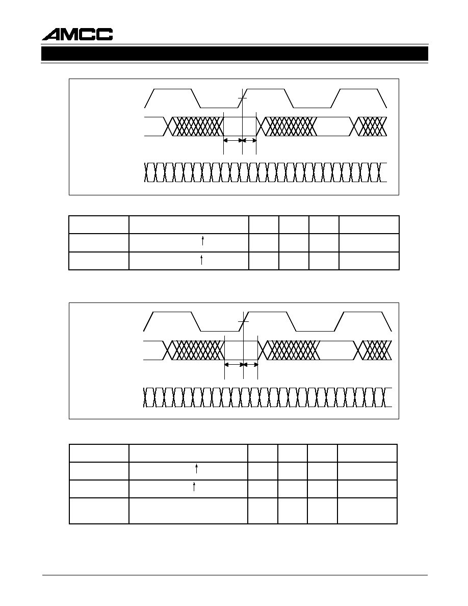
Figure 11. Transmitter Timing (TBC Mode, TMODE =1)
Table 13. S2078 Transmitter Timing (TBC Mode, TMODE =1)
TBCx
DINx[0:9]
T
1
T
2
SERIAL DATA OUT
s
r
e
t
e
m
a
r
a
P
n
o
i
t
p
i
r
c
s
e
D
n
i
M
x
a
M
s
t
i
n
U
s
n
o
i
t
i
d
n
o
C
T
1
C
B
T
.
t
.
r
.
w
p
u
t
e
S
a
t
a
D
0
.
1
s
n
.
1
e
t
o
N
e
e
S
T
2
C
B
T
.
t
.
r
.
w
d
l
o
H
a
t
a
D
5
.
0
s
n
x
C
B
T
n
e
e
w
t
e
b
t
f
i
r
d
e
s
a
h
P
K
L
C
F
E
R
d
n
a
3
-
3
+
s
n
1. All AC measurements are made from the reference voltage level of the clock (1.4V) to the valid input or output data
levels (.8V or 2.0V).
Figure 10. Transmitter Timing (REFCLK Mode, TMODE =0)
Table 12. S2078 Transmitter Timing (REFCLK Mode, TMODE = 0)
REFCLK
DINx[0:9]
T
1
T
2
SERIAL DATA OUT
s
r
e
t
e
m
a
r
a
P
n
o
i
t
p
i
r
c
s
e
D
n
i
M
x
a
M
s
t
i
n
U
s
n
o
i
t
i
d
n
o
C
T
1
K
L
C
F
E
R
.
t
.
r
.
w
p
u
t
e
S
a
t
a
D
5
.
0
s
n
.
1
e
t
o
N
e
e
S
T
2
K
L
C
F
E
R
.
t
.
r
.
w
d
l
o
H
a
t
a
D
3
.
1
s
n
1. All AC measurements are made from the reference voltage level of the clock (1.4V) to the valid input or output data
levels (.8V or 2.0V).

17
S2078
DUAL FIBRE CHANNEL TRANSCEIVER
June 20, 2000 / Revision B
s
r
e
t
e
m
a
r
a
P
n
o
i
t
p
i
r
c
s
e
D
n
i
M
x
a
M
s
t
i
n
U
s
n
o
i
t
i
d
n
o
C
T
3
K
L
C
F
E
R
.
t
.
r
.
w
O
K
L
C
T
2
5
.
7
s
n
e
l
c
y
C
y
t
u
D
O
K
L
C
T
%
0
4
%
0
6
%
Note: Measurements are made at 1.4V level of clocks.
Table 15. S2078 Transmitter (TCLKO Timing)
REFCLK
T
3
TCLKO
Figure 12. TCLKO Timing
Table 14. S2078 Transmitter Timing
s
r
e
t
e
m
a
r
a
P
n
o
i
t
p
i
r
c
s
e
D
n
i
M
x
a
M
s
t
i
n
U
s
n
o
i
t
i
d
n
o
C
T
R
D
S
T
,
F
D
S
ll
a
F
d
n
a
e
s
i
R
a
t
a
D
l
a
i
r
e
S
0
0
3
s
p
.
s
i
s
a
b
e
l
p
m
a
s
n
o
d
e
t
s
e
t
,
%
0
8
-
%
0
2
K
5
.
4
.
d
n
u
o
r
g
o
t
T
J
r
e
t
t
ij
l
a
t
o
t
t
u
p
t
u
O
a
t
a
D
l
a
i
r
e
S
)
p
-
p
(
3
2
.
0
I
U
e
l
p
m
a
s
n
o
d
e
r
u
s
a
e
m
,
k
a
e
p
-
o
t
-
k
a
e
P
2
r
o
5
.
8
2
K
±
h
t
i
w
d
e
r
u
s
a
e
M
.
s
i
s
a
b
7
1
-
.
z
H
G
2
6
0
.
1
t
a
n
r
e
t
t
a
p
T
J
D
t
u
p
t
u
O
a
t
a
D
l
a
i
r
e
S
)
p
-
p
(
r
e
t
t
ij
c
i
t
s
i
n
i
m
r
e
t
e
d
8
0
.
0
I
U
e
l
p
m
a
s
a
n
o
d
e
t
s
e
t
,
k
a
e
p
-
o
t
-
k
a
e
P
n
r
e
t
t
a
p
5
.
8
2
K
±
h
t
i
w
d
e
r
u
s
a
e
M
.
s
i
s
a
b
.
z
H
G
2
6
0
.
1
t
a

18
S2078
DUAL FIBRE CHANNEL TRANSCEIVER
June 20, 2000 / Revision B
Figure 13. Receiver Timing (Full Clock Mode, CMODE = 1)
Table 16. S2078 Receiver Timing (Full Clock Mode, CMODE = 1)
Table 17. S2078 Receiver Timing (Half Clock Mode, CMODE = 0)
RBC0x
DOUTx[0:9],
COM_DETx
SERIAL DATA IN
T
4
T
5
RBC1x
1. All AC measurements are made from the reference voltage level of the clock (1.4V) to the valid input or
output data levels (.8V or 2.0V).
RBC0x
DOUTx[0:9],
COM_DETx
SERIAL DATA IN
RBC1x
T
6
T
7
T
6
T
7
T
8
s
r
e
t
e
m
a
r
a
P
n
o
i
t
p
i
r
c
s
e
D
n
i
M
x
a
M
s
t
i
n
U
s
n
o
i
t
i
d
n
o
C
T
4
x
1
C
B
R
.
t
.
r
.
w
p
u
t
e
S
a
t
a
D
5
.
3
s
n
.
1
e
t
o
N
e
e
S
T
5
x
1
C
B
R
.
t
.
r
.
w
d
l
o
H
a
t
a
D
0
.
2
s
n
e
l
c
y
C
y
t
u
D
x
0
/
1
C
B
R
0
4
0
6
%
s
r
e
t
e
m
a
r
a
P
n
o
i
t
p
i
r
c
s
e
D
n
i
M
x
a
M
s
t
i
n
U
s
n
o
i
t
i
d
n
o
C
T
6
x
0
/
1
C
B
R
.
t
.
r
.
w
p
u
t
e
S
a
t
a
D
5
.
3
s
n
.
1
e
t
o
N
e
e
S
T
7
x
0
/
1
C
B
R
.
t
.
r
.
w
d
l
o
H
a
t
a
D
0
.
2
s
n
T
8
o
t
e
s
i
r
x
1
C
B
R
m
o
r
f
e
m
i
T
e
s
i
r
x
0
C
B
R
3
.
9
4
.
0
1
s
n
e
l
c
y
C
y
t
u
D
x
0
/
1
C
B
R
0
4
0
6
%
1. All AC measurements are made from the reference voltage level of the clock (1.4V) to the valid input or output data
levels (.8V or 2.0V).

19
S2078
DUAL FIBRE CHANNEL TRANSCEIVER
June 20, 2000 / Revision B
OTHER OPERATING MODES
Loopback Mode
When loopback mode is enabled, the serial data
from the transmitter is provided to the serial input of
the receiver. Loopback mode can be simultaneously
enabled for both channels using the loopback-en-
able input, LPEN.
The loopback mode provides the ability to perform
system diagnostics and off-line testing of the inter-
face to guarantee the integrity of the serial channel
before enabling the transmission medium.
Note that the high speed outputs are disabled during
loopback operation.
Test Modes
The RESET pin is used to initialize the transmit
FIFOs and must be asserted (LOW) prior to entering
the normal operational state (see section Transmit
FIFO Initialization).
Operating Frequency Rate
The S2078 is designed to operate at the Fibre Chan-
nel rate of 1.062 GHz.
output
disabled
CRU
CSU
Figure 15. S2078 Diagnostic Loopback Operation
Table 18. S2078 Receiver Timing
s
r
e
t
e
m
a
r
a
P
n
o
i
t
p
i
r
c
s
e
D
n
i
M
x
a
M
s
t
i
n
U
s
n
o
i
t
i
d
n
o
C
T
R
C
R
T
,
F
C
R
e
m
i
T
ll
a
F
d
n
a
e
s
i
R
0
C
B
R
,
1
C
B
R
4
.
2
s
n
.
V
0
.
2
+
o
t
V
8
.
+
d
e
r
u
s
a
e
M
.
7
1
e
r
u
g
i
F
e
e
S
T
R
D
T
,
F
D
e
m
i
T
ll
a
F
d
n
a
e
s
i
R
t
u
p
t
u
O
a
t
a
D
0
.
3
s
n
.
V
0
.
2
+
o
t
V
8
.
+
d
e
r
u
s
a
e
M
.
6
1
e
r
u
g
i
F
e
e
S
T
K
C
O
L
)
p
u
t
r
a
t
s
(
e
m
i
T
k
c
o
L
n
o
i
t
i
s
i
u
q
c
A
p
u
t
r
a
t
S
)
G
2
6
0
.
1
(
5
.
2
s
µ
.
p
u
r
e
w
o
p
r
e
t
f
A
T
J
D
F
r
e
t
t
i
J
t
n
e
d
n
e
p
e
D
y
c
n
e
u
q
e
r
F
e
c
n
a
r
e
l
o
T
0
1
.
0
I
U
.
1
1
T
3
X
I
S
N
A
n
i
d
e
i
f
i
c
e
p
s
s
A
T
J
D
e
c
n
a
r
e
l
o
T
r
e
t
t
i
J
t
u
p
n
I
c
i
t
s
i
n
i
m
r
e
t
e
D
8
3
.
0
I
U
.
1
1
T
3
X
I
S
N
A
n
i
d
e
i
f
i
c
e
p
s
s
A
T
J
R
e
c
n
a
r
e
l
o
T
r
e
t
t
i
J
t
u
p
n
I
m
o
d
n
a
R
2
2
.
0
I
U
.
1
1
T
3
X
I
S
N
A
n
i
d
e
i
f
i
c
e
p
s
s
A
T
J
e
c
n
a
r
e
l
o
T
r
e
t
t
i
J
t
u
p
n
I
l
a
t
o
T
7
.
0
I
U
.
1
1
T
3
X
I
S
N
A
n
i
d
e
i
f
i
c
e
p
s
s
A

20
S2078
DUAL FIBRE CHANNEL TRANSCEIVER
June 20, 2000 / Revision B
Table 19. Absolute Maximum Ratings
Table 20. Recommended Operating Conditions
Table 21. Reference Clock Requirements
r
e
t
e
m
a
r
a
P
n
i
M
p
y
T
x
a
M
s
t
i
n
U
s
a
i
B
r
e
d
n
U
e
r
u
t
a
r
e
p
m
e
T
e
s
a
C
5
5
≠
5
2
1
C
∞
s
a
i
B
r
e
d
n
U
e
r
u
t
a
r
e
p
m
e
T
n
o
i
t
c
n
u
J
5
5
≠
0
5
1
C
∞
e
r
u
t
a
r
e
p
m
e
T
e
g
a
r
o
t
S
5
6
≠
0
5
1
C
∞
D
N
G
o
t
t
c
e
p
s
e
R
h
t
i
w
D
D
V
n
o
e
g
a
t
l
o
V
5
.
0
≠
0
.
7
+
V
n
i
P
t
u
p
n
I
L
T
T
y
n
a
n
o
e
g
a
t
l
o
V
5
.
0
≠
7
4
.
3
V
n
i
P
t
u
p
n
I
L
C
E
P
y
n
a
n
o
e
g
a
t
l
o
V
0
D
D
V
V
t
n
e
r
r
u
C
k
n
i
S
t
u
p
t
u
O
L
T
T
8
A
m
t
n
e
r
r
u
C
e
c
r
u
o
S
t
u
p
t
u
O
L
T
T
8
A
m
t
n
e
r
r
u
C
e
c
r
u
o
S
t
u
p
t
u
O
L
C
E
P
d
e
e
p
S
h
g
i
H
0
3
A
m
O
/
I
L
T
T
,
e
g
a
t
l
o
V
e
g
r
a
h
c
s
i
D
c
i
t
a
t
S
0
0
0
2
V
O
/
I
L
C
E
P
,
e
g
a
t
l
o
V
e
g
r
a
h
c
s
i
D
c
i
t
a
t
S
0
0
5
1
V
r
e
t
e
m
a
r
a
P
n
i
M
p
y
T
x
a
M
s
t
i
n
U
s
a
i
B
r
e
d
n
U
e
r
u
t
a
r
e
p
m
e
T
t
n
e
i
b
m
A
0
0
7
C
∞
s
a
i
B
r
e
d
n
U
e
r
u
t
a
r
e
p
m
e
T
n
o
i
t
c
n
u
J
0
3
1
C
∞
o
t
t
c
e
p
s
e
r
h
t
i
w
n
i
p
r
e
w
o
p
y
n
a
n
o
e
g
a
t
l
o
V
S
S
V
/
D
N
G
3
1
.
3
3
.
3
7
4
.
3
V
n
i
P
t
u
p
n
I
L
T
T
n
o
e
g
a
t
l
o
V
0
7
4
.
3
V
n
i
P
t
u
p
n
I
L
C
E
P
y
n
a
n
o
e
g
a
t
l
o
V
D
D
V
V
2
≠
D
D
V
V
s
r
e
t
e
m
a
r
a
P
n
o
i
t
p
i
r
c
s
e
D
n
i
M
x
a
M
s
t
i
n
U
s
n
o
i
t
i
d
n
o
C
T
F
e
c
n
a
r
e
l
o
T
y
c
n
e
u
q
e
r
F
0
0
1
≠
0
0
1
+
m
p
p
D
T
2
-
1
y
r
t
e
m
m
y
S
0
4
0
6
%
.
t
p
%
0
5
t
a
e
l
c
y
C
y
t
u
D
T
R
C
R
T
,
F
C
R
e
m
i
T
ll
a
F
d
n
a
e
s
i
R
K
L
C
F
E
R
2
s
n
.
%
0
8
≠
%
0
2
--
r
e
t
t
i
J
0
8
s
p
.
e
y
e
a
t
a
d
%
7
7
,
k
a
e
P
-
o
t
-
k
a
e
P

21
S2078
DUAL FIBRE CHANNEL TRANSCEIVER
June 20, 2000 / Revision B
Table 22. DC Characteristics
s
r
e
t
e
m
a
r
a
P
n
o
i
t
p
i
r
c
s
e
D
n
i
M
p
y
T
x
a
M
s
t
i
n
U
s
n
o
i
t
i
d
n
o
C
V
H
O
)
L
T
T
(
e
g
a
t
l
o
V
h
g
i
H
t
u
p
t
u
O
4
.
2
8
.
2
D
D
V
V
I
n
i
m
=
D
D
V
H
O
A
m
4
-
=
V
L
O
)
L
T
T
(
e
g
a
t
l
o
V
w
o
L
t
u
p
t
u
O
D
N
G
5
2
0
.
5
.
0
V
I
n
i
m
=
D
D
V
L
O
A
m
4
=
V
H
I
)
L
T
T
(
e
g
a
t
l
o
V
h
g
i
H
t
u
p
n
I
0
.
2
V
V
L
I
)
L
T
T
(
e
g
a
t
l
o
V
w
o
L
t
u
p
n
I
D
N
G
8
.
0
V
I
H
I
)
L
T
T
(
t
n
e
r
r
u
C
h
g
i
H
t
u
p
n
I
0
4
A
µ
V
N
I
x
a
M
=
D
D
V
,
V
4
.
2
=
I
L
I
)
L
T
T
(
t
n
e
r
r
u
C
w
o
L
t
u
p
n
I
0
0
6
A
µ
V
N
I
x
a
M
=
D
D
V
,
V
8
.
0
=
D
D
I
t
n
e
r
r
u
C
y
l
p
p
u
S
2
0
4
0
0
5
A
m
.
n
r
e
t
t
a
P
0
1
0
1
P
D
n
o
i
t
a
p
i
s
s
i
D
r
e
w
o
P
3
3
.
1
4
7
.
1
W
.
n
r
e
t
t
a
P
0
1
0
1
V
F
F
I
D
g
n
i
w
s
e
g
a
t
l
o
v
t
u
p
n
i
l
a
i
t
n
e
r
e
f
f
i
d
.
n
i
M
s
t
u
p
n
i
L
C
E
P
l
a
i
t
n
e
r
e
f
f
i
d
r
o
f
0
0
1
0
0
2
2
V
m
.
9
1
e
r
u
g
i
F
e
e
S
V
T
U
O
e
g
a
t
l
o
V
t
u
p
t
u
O
l
a
i
r
e
S
l
a
i
t
n
e
r
e
f
f
i
D
g
n
i
w
S
0
0
5
1
0
0
9
1
0
0
2
2
V
m
K
5
.
4
h
t
i
w
d
e
l
p
u
o
c
C
A
0
0
1
d
n
a
n
w
o
d
ll
u
p
.
n
o
i
t
a
n
i
m
r
e
t
l
a
i
t
n
e
r
e
f
f
i
d
.
8
1
e
r
u
g
i
F
e
e
S
C
N
I
e
c
n
a
t
i
c
a
p
a
C
t
u
p
n
I
3
f
p
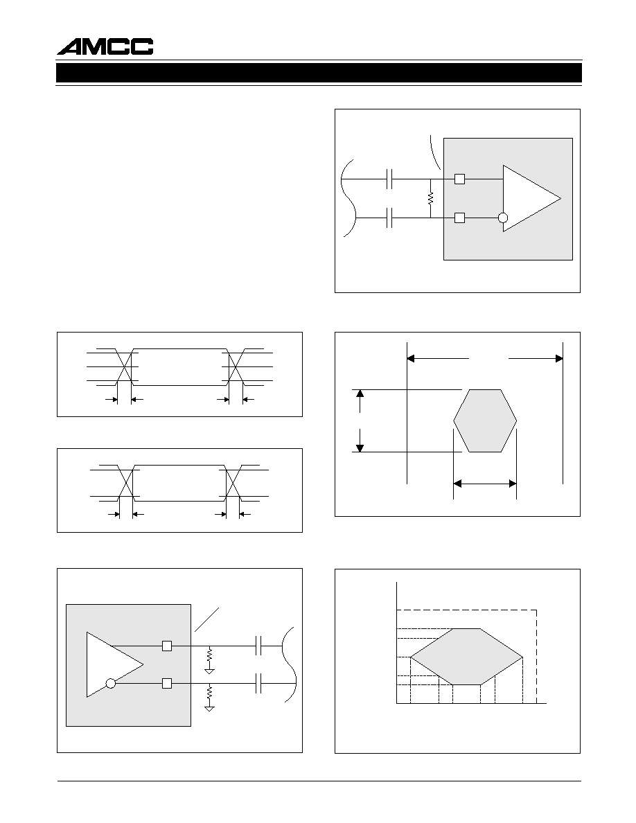
22
S2078
DUAL FIBRE CHANNEL TRANSCEIVER
June 20, 2000 / Revision B
OUTPUT LOAD
The S2078 serial outputs require a resistive load to
set the output current. The recommended resistor
value is 4.5K
to ground. This value can be varied
to adjust drive current, signal voltage swing, and
power usage on the board.
ACQUISITION TIME
With the input eye diagram shown in Figure 21, the
S2078 will recover data with a
1E-9 BER within the
time specified by T
LOCK
in Table 18 after an instan-
taneous phase shift of the incoming data.
Figure 19. High Speed Differential Inputs
Figure 16. Serial Input/Output Rise and Fall Time
Figure 20. Receiver Input Eye Diagram Jitter Mask
Figure 17. TTL Input/Output Rise and Fall Time
Figure 18. Serial Output Load
Figure 21. Acquisition Time Eye Diagram
T
r
T
f
80%
20%
50%
80%
20%
50%
T
r
T
f
+2.0V
+0.8V
+2.0V
+0.8V
4.5K
4.5K
0.01
µ
f
0.01
µ
f
Vcc ≠1.3V
100
0.01
µ
f
0.01
µ
f
Vcc ≠ 1.3 V
Bit Time
Amplitude
30%
1.3
Normalized Amplitude
Normalized Time
1.0
0.0
0.2
0.3
0.5
0.7
0.8
0.1
0.6
0.4
0.3
0.7
0.9
1.0
0.0
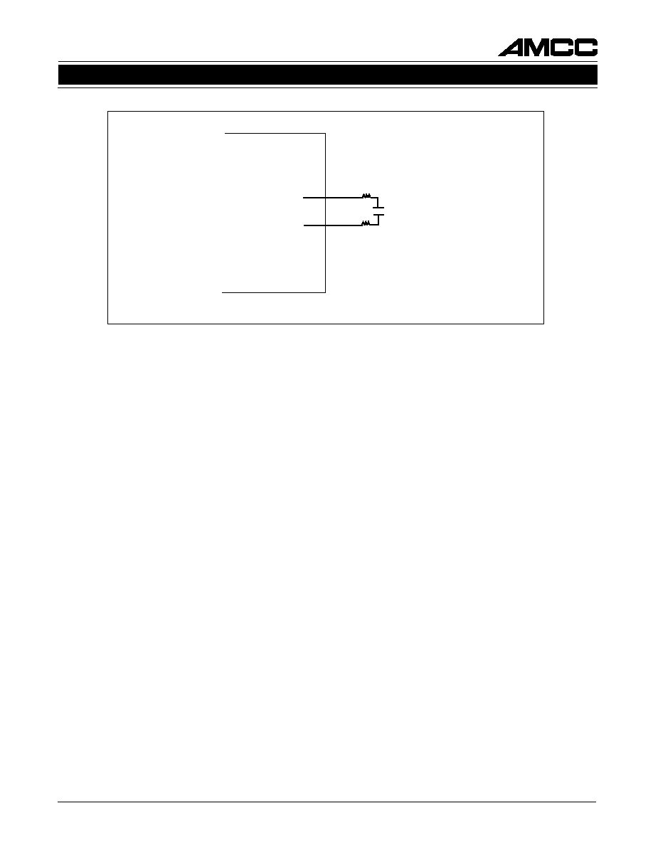
23
S2078
DUAL FIBRE CHANNEL TRANSCEIVER
June 20, 2000 / Revision B
Figure 22. Loop Filter Capacitor Connections
CAP1
270
22 nf
CAP2
270
S2078
24
S2078
DUAL FIBRE CHANNEL TRANSCEIVER
June 20, 2000 / Revision B
Ordering Information
X
XXXX
XX
Prefix Device Package
AMCC is a registered trademark of Applied Micro Circuits Corporation.
Copyright Æ 2000 Applied Micro Circuits Corporation
AMCC reserves the right to make changes to its products or to discontinue any semiconductor product or service without notice, and
advises its customers to obtain the latest version of relevant information to verify, before placing orders, that the information being relied
on is current.
AMCC does not assume any liability arising out of the application or use of any product or circuit described herein, neither does it
convey any license under its patent rights nor the rights of others.
AMCC reserves the right to ship devices of higher grade in place of those of lower grade.
AMCC SEMICONDUCTOR PRODUCTS ARE NOT DESIGNED, INTENDED, AUTHORIZED, OR WARRANTED TO BE SUITABLE FOR
USE IN LIFE-SUPPORT APPLICATIONS, DEVICES OR SYSTEMS OR OTHER CRITICAL APPLICATIONS.
Applied Micro Circuits Corporation ∑ 6290 Sequence Dr., San Diego, CA 92121
Phone: (858) 450-9333 ∑ (800) 755-2622 ∑ Fax: (858) 450-9885
http://www.amcc.com
C
E
R T I F I E
D
IS
O 9001
X
I
F
E
R
P
E
C
I
V
E
D
E
G
A
K
C
A
P
t
i
u
c
r
i
C
d
e
t
a
r
g
e
t
n
I
≠
S
8
7
0
2
A
G
B
T
6
5
1
≠
B
T