 | –≠–ª–µ–∫—Ç—Ä–æ–Ω–Ω—ã–π –∫–æ–º–ø–æ–Ω–µ–Ω—Ç: S2092 | –°–∫–∞—á–∞—Ç—å:  PDF PDF  ZIP ZIP |

1
S2092
SERIAL BACKPLANE RETIMER DEVICE
July 10, 2000 / Revision A
BiCMOS PECL CLOCK GENERATOR
DEVICE
SPECIFICATION
SERIAL BACKPLANE RETIMER DEVICE
S2092
Æ
FEATURES
∑
On-chip high frequency PLL with internal
loop filter for clock recovery
∑
Internal 100
line-to-line termination on
high speed differential input
∑
Supports data recovery from:
2.488 to 2.67 Gbps (2.488 Gbps with FEC
overhead data rate capability)
∑
Selectable reference frequencies
∑
Lock detect--monitors frequency of
incoming data
∑
Low-jitter serial CML interface
∑
Single +3.3 V supply, 455 mW power
dissipation (typ)
∑
Compact 7 mm x 7 mm 48 pin TQFP/TEP
package
APPLICATIONS
∑
Dense Wavelength Division Multiplexing
(DWDM) systems
∑
Serial Backplane interfaces
∑
2.488 Gbps to 2.67 Gbps Short Haul
Retiming
∑
Crosspoint interfaces
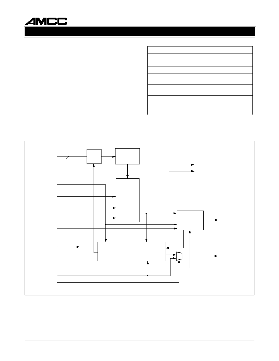
GENERAL DESCRIPTION
The function of the S2092 retimer device is to derive
high speed timing signals for DWDM equipment. The
S2092 is implemented using AMCC's proven Phase
Lock Loop (PLL) technology. Figure 1 shows a typical
network application.
The S2092 can receive a 2.488 Gbps to 2.67 Gbps
scrambled NRZ signal. This range is dependent on
the user's FEC needs and reference frequency selec-
tion. The S2092 recovers the clock from the data
and outputs the retimed data.
The S2092 utilizes an on-chip PLL which consists
of a phase detector, a loop filter, and a Voltage
Controlled Oscillator (VCO). The phase detector
compares the phase relationship between the VCO
output and the serial data input. A loop filter con-
verts the phase detector output into a smooth DC
voltage, and the DC voltage is input to the VCO
whose frequency is varied by this voltage. A block
diagram is shown in Figure 2.
Figure 1. System Block Diagram
S3057
S3057
S3057
S3052
S3057
S3056
S3056
S3056
S3056
Port Card
Port Card
Port Card
S2018
Switch Card
S2092
S2092
S2092
S2092
S2092
S2092
S2092
S2092
S3057
S3057
S3052
S3057
S3057
S3057
S3052
S3057
S3056
S3056
Port Card
S3052
S3052
S3052
S3056
S3056
S3057
S3057
S3052
S3052
2
S2092
SERIAL BACKPLANE RETIMER DEVICE
July 10, 2000 / Revision A
S2092 OVERVIEW
The S2092 supports clock recovery from 2.488 Gbps
to 2.67 Gbps data rate. Differential serial data is input
to the chip at the specified rate, and clock recovery is
performed on the incoming data stream. An external
oscillator is required to minimize the PLL lock time.
Retimed data is output from the S2092.
Figure 2. S2092 Functional Block Diagram
2
LOCKDET
SERDATOP/N
REFCLKP/N
TESTCLK
LCKREFN
SERDATIP/N
LOOP
FILTER
VCO
CLOCK
DIVIDER
PHASE DETECTOR
LOCK
DETECTOR
SDN
CAP 1,2
REFSEL
TESTEN
RST
BYPASS
TESTOUT 1
TESTOUT 2
Suggested Interface Devices
C
C
M
A
8
1
0
2
S
1
h
c
t
i
w
S
t
n
i
o
p
s
s
o
r
C
s
p
b
G
2
.
3
7
1
x
7
C
C
M
A
3
8
0
3
S
r
e
t
t
i
m
s
n
a
r
T
1
:
6
1
8
4
-
C
O
C
C
M
A
3
6
0
3
S
r
e
t
t
i
m
s
n
a
r
T
1
:
6
1
l
a
i
t
n
e
r
e
f
f
i
D
8
4
-
C
O
C
C
M
A
4
4
0
3
S
r
e
v
i
e
c
e
R
6
1
:
1
8
4
-
C
O
C
C
M
A
7
5
0
3
S
M
T
A
/
H
D
S
/
T
E
N
O
S
e
t
a
R
-
i
t
l
u
M
r
e
v
i
e
c
s
n
a
r
T
C
C
M
A
7
6
0
3
S
M
T
A
/
H
D
S
/
T
E
N
O
S
e
t
a
R
-
i
t
l
u
M
C
E
F
/
w
r
e
v
i
e
c
s
n
a
r
T
C
C
M
A
6
5
0
3
S
a
t
a
D
d
n
a
k
c
o
l
C
e
t
a
R
-
t
il
u
M
t
i
n
U
y
r
e
v
o
c
e
R
C
C
M
A
2
5
0
3
S
r
o
t
i
n
o
M
e
c
n
a
m
r
o
f
r
e
P
e
t
a
R
-
t
il
u
M
3
S2092
SERIAL BACKPLANE RETIMER DEVICE
July 10, 2000 / Revision A
S2092 FUNCTIONAL DESCRIPTION
The S2092 retimer device performs clock recovery
function from 2.488 Gbps to 2.67 Gbps serial data
links. The chip extracts the clock from the serial data
inputs and provides retimed data outputs. A 155.52
to 166.63 or 19.44 to 20.83 MHz reference clock is
required (REFCLK frequency is dependent on which
FEC capability is required. See Table 2 for the
number of bytes per 255 byte block to set the proper
reference frequency.) for phase lock loop start up
and proper operation under loss of signal conditions.
An integral prescaler and phase lock loop circuit is
used to multiply this reference to the nominal bit rate.
Data Retiming
Data retiming, as shown in the block diagram in Fig-
ure 2, generates a clock that is at the same fre-
quency as the incoming data bit rate at the serial
data input. The clock is phase aligned by a PLL so
that it samples the data in the center of the data eye
pattern.
The phase relationship between the edge transi-
tions of the data and those of the generated clock
are compared by a phase/frequency discriminator.
Output pulses from the discriminator indicate the
required direction of phase corrections. These
pulses are smoothed by an integral loop filter. The
output of the loop filter controls the frequency of
the Voltage Controlled Oscillator (VCO), which
generates the recovered clock.
Table 1. Reference Frequency Select
Frequency stability without incoming data is guaran-
teed by an alternate reference input (REFCLK) that
the PLL locks onto when data is lost. If the frequency
of the incoming signal varies by a value greater than
that stated in Table 7 with respect to REFCLKP/N,
the PLL will be declared out of lock, and the PLL will
lock to the reference clock. The assertion of SDN will
also cause an out of lock condition.
The loop filter transfer function is optimized to enable
the PLL to track the jitter, yet tolerate the minimum
transition density in a received data signal.
Lock Detect
The S2092 contains a lock detect circuit which monitors
the integrity of the serial data inputs. If the received
serial data fails the frequency test, the PLL will be
forced to lock to the local reference clock. This will
maintain the correct frequency of the recovered clock
output under loss of signal or loss of lock conditions. If
the recovered clock frequency deviates from the local
reference clock frequency by more than that stated in
Table 7, the PLL will be declared out of lock. The lock
detect circuit will poll the input data stream in an attempt
to reacquire lock to data. If the recovered clock fre-
quency is determined to be within that range stated in
Table 7, the PLL will be declared in lock and the lock
detect output will go active. The assertion of SDN will
also cause an out of lock condition.
L
E
S
F
E
R
y
c
n
e
u
q
e
r
F
e
c
n
e
r
e
f
e
R
0
z
H
M
3
8
.
0
2
o
t
4
4
.
9
1
1
z
H
M
3
6
.
6
6
1
o
t
2
5
.
5
5
1
L
E
S
F
E
R
k
c
o
l
B
e
t
y
B
≠
5
5
2
r
e
p
s
e
t
y
b
X
f
o
y
t
i
l
i
b
a
p
a
C
C
E
F
h
t
i
w
s
e
t
a
R
a
t
a
D
r
o
f
y
c
n
e
u
q
e
r
F
e
c
n
e
r
e
f
e
R
0
=
X
3
=
X
4
=
X
5
=
X
6
=
X
7
=
X
8
=
X
0
z
H
M
4
4
.
9
1
z
H
M
9
9
.
9
1
z
H
M
5
1
.
0
2
z
H
M
1
3
.
0
2
z
H
M
8
4
.
0
2
z
H
M
5
6
.
0
2
z
H
M
3
8
.
0
2
1
z
H
M
2
5
.
5
5
1
z
H
M
1
9
.
9
5
1
z
H
M
1
2
.
1
6
1
z
H
M
3
5
.
2
6
1
z
H
M
7
8
.
3
6
1
z
H
M
6
2
.
5
6
1
z
H
M
3
6
.
6
6
1
Table 2. FEC Modes

4
S2092
SERIAL BACKPLANE RETIMER DEVICE
July 10, 2000 / Revision A
CHARACTERISTICS
Input Jitter Tolerance
Input jitter tolerance is defined as the peak to
peak amplitude of sinusoidal jitter applied on the
input signal that causes an equivalent 1 dB opti-
cal/electrical power penalty. See Figure 3.
Jitter Transfer
The jitter transfer function is defined as the ratio of
jitter on the output signal to the jitter applied on the
input signal versus frequency. Jitter transfer require-
ments are shown in Figure 4. The measurement con-
dition is that input sinusoidal jitter up to the mask
level in Figure 4 be applied.
Jitter Generation
The jitter of the serial data outputs shall not exceed
the value specified in Table 7. The conditions are
stated with a serial data input with no jitter presented
on SERDATIP/N. (See Table 7).
Figure 3. Input Jitter Tolerance Specification
Figure 4. Jitter Transfer Specification
f0
f1
f2
f3
ft
0.15
1.5
15
Sinusodal
Input Jitter
Amplitude
(UI p-p)
fc
P
Jitter
Transfer
Frequency
Acceptable
Range
slope = -20 dB/decade
e
t
a
R
a
t
a
D
0
f
)
z
H
(
1
f
)
z
H
(
2
f
)
z
H
(
3
f
)
z
H
k
(
t
f
)
z
H
k
(
s
p
b
G
8
8
4
.
2
0
1
0
0
6
0
0
0
6
0
0
1
0
0
0
1
e
t
a
R
a
t
a
D
c
f
)
z
H
k
(
P
)
B
d
(
s
p
b
G
8
8
4
.
2
0
0
0
2
1
.
0

5
S2092
SERIAL BACKPLANE RETIMER DEVICE
July 10, 2000 / Revision A
Table 3. Pin Assignment and Descriptions
e
m
a
N
n
i
P
l
e
v
e
L
O
/
I
#
n
i
P
n
o
i
t
p
i
r
c
s
e
D
P
I
T
A
D
R
E
S
N
I
T
A
D
R
E
S
.
f
f
i
D
L
M
C
I
3
2
.
s
t
u
p
n
i
e
s
e
h
t
n
o
s
n
o
i
t
i
s
n
a
r
t
e
h
t
m
o
r
f
d
e
r
e
v
o
c
e
r
s
i
k
c
o
l
C
.
n
I
a
t
a
D
l
a
i
r
e
S
)
.
8
e
r
u
g
i
F
e
e
S
(
.
d
e
t
a
n
i
m
r
e
t
d
n
a
d
e
s
a
i
b
y
ll
a
n
r
e
t
n
I
S
S
A
P
Y
B
L
T
T
V
L
I
6
4
a
t
a
d
e
h
t
f
o
n
o
i
s
s
i
m
s
n
a
r
t
s
w
o
ll
a
t
I
.
L
L
P
e
h
t
s
s
a
p
y
b
o
t
d
e
s
U
.
h
g
i
H
e
v
i
t
c
A
.
y
r
e
v
o
c
e
r
k
c
o
l
c
t
u
o
h
t
i
w
t
u
p
n
i
N
D
S
e
l
g
n
i
S
d
e
d
n
E
L
C
E
P
V
L
I
5
4
n
e
v
i
r
d
e
b
o
t
t
u
p
n
i
L
C
E
P
K
0
1
d
e
d
n
e
-
e
l
g
n
i
s
A
.
w
o
L
e
v
i
t
c
A
.
t
c
e
t
e
D
l
a
n
g
i
S
d
e
v
i
e
c
e
r
f
o
s
s
o
l
a
e
t
a
c
i
d
n
i
o
t
e
l
u
d
o
m
r
e
v
i
e
c
e
r
l
a
c
i
t
p
o
l
a
n
r
e
t
x
e
e
h
t
y
b
n
I
a
t
a
D
l
a
i
r
e
S
e
h
t
n
o
a
t
a
d
e
h
t
,
e
v
i
t
c
a
n
i
s
i
N
D
S
n
e
h
W
.
r
e
w
o
p
l
a
c
i
t
p
o
e
h
t
d
n
a
o
r
e
z
t
n
a
t
s
n
o
c
a
o
t
d
e
c
r
o
f
y
ll
a
n
r
e
t
n
i
e
b
ll
i
w
s
n
i
p
)
N
/
P
I
T
A
D
R
E
S
(
,
e
v
i
t
c
a
s
i
N
D
S
n
e
h
W
.
t
u
p
n
i
K
L
C
F
E
R
e
h
t
o
t
k
c
o
l
o
t
d
e
c
r
o
f
e
b
ll
i
w
L
L
P
.
y
ll
a
m
r
o
n
d
e
s
s
e
c
o
r
p
e
b
ll
i
w
s
n
i
p
N
/
P
I
T
A
D
R
E
S
e
h
t
n
o
a
t
a
d
P
K
L
C
F
E
R
N
K
L
C
F
E
R
y
ll
a
n
r
e
t
n
I
d
e
s
a
i
B
.
f
f
i
D
L
C
E
P
V
L
I
6
7
s
e
l
b
a
T
e
e
s
(
z
H
M
3
8
.
0
2
o
t
4
4
.
9
1
r
o
3
6
.
6
6
1
o
t
2
5
.
5
5
1
.
k
c
o
l
C
e
c
n
e
r
e
f
e
R
o
t
d
e
s
u
t
u
p
n
i
)
s
e
i
c
n
e
u
q
e
r
f
k
c
o
l
c
e
c
n
e
r
e
f
e
r
l
a
n
o
i
t
i
d
d
a
r
o
f
2
d
n
a
1
d
n
a
L
L
P
y
r
e
v
o
c
e
r
k
c
o
l
c
e
h
t
f
o
y
c
n
e
u
q
e
r
f
g
n
i
t
a
r
e
p
o
l
a
i
t
i
n
i
e
h
t
h
s
il
b
a
t
s
e
r
o
,
t
e
s
e
r
g
n
i
r
u
d
,
a
t
a
d
f
o
e
c
n
e
s
b
a
e
h
t
n
i
k
c
o
l
c
y
b
d
n
a
t
s
a
s
a
d
e
s
u
o
s
l
a
.
d
e
s
a
i
b
y
ll
a
n
r
e
t
n
I
.
e
v
i
t
c
a
n
i
s
i
N
D
S
n
e
h
w
1
P
A
C
2
P
A
C
I
0
4
9
3
s
r
o
t
s
i
s
e
r
d
n
a
r
o
t
i
c
a
p
a
c
r
e
t
li
f
p
o
o
l
l
a
n
r
e
t
x
e
e
h
T
.
r
o
t
i
c
a
p
a
C
r
e
t
li
F
p
o
o
L
)
.
1
1
e
r
u
g
i
F
e
e
S
(
.
s
n
i
p
e
s
e
h
t
o
t
d
e
t
c
e
n
n
o
c
e
r
a
N
F
E
R
K
C
L
L
T
T
V
L
I
7
1
ll
i
w
t
u
p
t
u
o
a
t
a
d
l
a
i
r
e
s
e
h
t
,
e
v
i
t
c
a
n
e
h
W
.
w
o
L
e
v
i
t
c
A
.
e
c
n
e
r
e
f
e
R
o
t
k
c
o
L
.
d
il
a
v
n
i
e
b
K
L
C
T
S
E
T
L
T
T
V
L
I
5
1
C
D
o
n
(
n
e
p
o
e
v
a
e
L
.
t
s
e
t
n
o
i
t
c
u
d
o
r
p
r
o
f
d
e
s
u
l
a
n
g
i
s
t
u
p
n
i
t
s
e
T
.
n
o
i
t
a
r
e
p
o
l
a
m
r
o
n
r
o
f
)
n
o
i
t
c
e
n
n
o
c
L
E
S
F
E
R
L
T
T
V
L
I
8
1
)
.
2
d
n
a
1
s
e
l
b
a
T
e
e
S
(
y
c
n
e
u
q
e
r
f
e
c
n
e
r
e
f
e
r
e
h
t
s
t
c
e
l
e
S
T
S
R
L
T
T
V
L
I
6
1
r
o
f
t
i
u
c
r
i
c
N
-
y
b
-
e
d
i
v
i
d
O
C
V
d
n
a
t
i
u
c
r
i
c
t
c
e
t
e
d
k
c
o
l
s
t
e
s
e
R
.
h
g
i
H
e
v
i
t
c
A
.
t
s
e
t
n
o
i
t
c
u
d
o
r
p
N
E
T
S
E
T
L
T
T
V
L
I
7
4
e
i
T
.
t
s
e
t
n
o
i
t
c
u
d
o
r
p
r
o
f
O
C
V
e
h
t
s
e
s
s
a
p
y
B
.
h
g
i
H
e
v
i
t
c
A
.
e
l
b
a
n
E
t
s
e
T
.
n
o
i
t
a
r
e
p
o
l
a
m
r
o
n
r
o
f
w
o
L
P
O
T
A
D
R
E
S
N
O
T
A
D
R
E
S
.
f
f
i
D
L
M
C
O
8
2
7
2
a
t
a
d
g
n
i
m
o
c
n
i
e
h
t
f
o
n
o
i
s
r
e
v
d
e
y
a
l
e
d
e
h
t
s
i
l
a
n
g
i
s
s
i
h
T
.
t
u
O
a
t
a
D
l
a
i
r
e
S
.
)
I
T
A
D
R
E
S
(
m
a
e
r
t
s
T
E
D
K
C
O
L
L
T
T
V
L
O
0
1
k
c
o
l
c
l
a
n
r
e
t
n
i
e
h
t
n
e
h
w
h
g
i
H
t
e
S
.
r
o
t
a
c
i
d
n
i
y
r
e
v
o
c
e
r
k
c
o
l
C
.
t
c
e
t
e
D
k
c
o
L
n
a
s
i
T
E
D
K
C
O
L
.
m
a
e
r
t
s
a
t
a
d
g
n
i
m
o
c
n
i
e
h
t
o
t
n
o
d
e
k
c
o
l
s
a
h
y
r
e
v
o
c
e
r
.
t
u
p
t
u
o
s
u
o
n
o
r
h
c
n
y
s
a
1
T
U
O
T
S
E
T
O
3
2
.
n
o
i
t
a
r
e
p
o
l
a
m
r
o
n
r
o
f
)
n
o
i
t
c
e
n
n
o
c
C
D
o
n
(
n
e
p
o
e
v
a
e
L
.
t
u
p
t
u
O
t
s
e
T
2
T
U
O
T
S
E
T
O
3
3
.
n
o
i
t
a
r
e
p
o
l
a
m
r
o
n
r
o
f
)
n
o
i
t
c
e
n
n
o
c
C
D
o
n
(
n
e
p
o
e
v
a
e
L
.
t
u
p
t
u
O
t
s
e
T
1
E
D
O
M
T
S
E
T
L
T
T
V
L
I
9
1
.
n
o
i
t
a
r
e
p
o
l
a
m
r
o
n
r
o
f
h
g
i
H
p
e
e
K
.
l
o
r
t
n
o
C
e
d
o
M
t
s
e
T
2
E
D
O
M
T
S
E
T
L
T
T
V
L
I
0
2
.
n
o
i
t
a
r
e
p
o
l
a
m
r
o
n
r
o
f
h
g
i
H
p
e
e
K
.
l
o
r
t
n
o
C
e
d
o
M
t
s
e
T

6
S2092
SERIAL BACKPLANE RETIMER DEVICE
July 10, 2000 / Revision A
e
m
a
N
n
i
P
.
y
t
Q
#
n
i
P
n
o
i
t
p
i
r
c
s
e
D
C
C
V
A
2
2
4
,
7
3
.
y
l
p
p
u
s
r
e
w
o
p
g
o
l
a
n
A
V
3
.
3
+
D
N
G
A
3
3
4
,
1
4
,
8
3
.
n
o
i
t
c
e
n
n
o
c
D
N
G
g
o
l
a
n
A
C
C
V
8
,
4
2
,
1
2
,
9
,
5
,
1
8
4
,
9
2
,
6
2
.
y
l
p
p
u
S
r
e
w
o
P
V
3
.
3
+
D
N
G
2
1
,
3
1
,
2
1
,
1
1
,
8
,
4
,
0
3
,
5
2
,
2
2
,
4
1
4
4
,
6
3
,
1
3
.
n
o
i
t
c
e
n
n
o
c
d
n
u
o
r
G
C
N
D
3
5
3
,
4
3
,
2
3
.
s
n
i
p
t
s
e
t
s
a
d
e
s
U
.
t
c
e
n
n
o
c
t
o
n
o
D
Table 3. Pin Assignment and Descriptions (Continued)

7
S2092
SERIAL BACKPLANE RETIMER DEVICE
July 10, 2000 / Revision A
Figure 5. S2092 Pinout
Note: DNC used as test pins.
1
2
3
4
5
7
9
11
36
35
34
33
31
29
27
25
32
30
28
26
23
24
22
21
20
19
18
17
16
15
13
14
38
37
39
40
41
42
43
44
45
46
48
47
12
8
10
6
SERDATIN
SERDATIP
GND
VCC
VCC
GND
GND
LOCKDET
VCC
TESTEN
BYPASS
SDN
AGND
GND
AVCC
AGND
CAP1
CAP2
AVCC
AGND
GND
GND
TESTCLK
RST
LCKREFN
REFSEL
TESTMODE1
TESTMODE2
VCC
GND
VCC
TESTOUT1
GND
DNC
DNC
TESTOUT2
GND
VCC
SERDATON
GND
DNC
GND
SERDATOP
VCC
VCC
REFCLKN
GND
REFCLKP
S2092
48 Pin TQFP/TEP
Top View

8
S2092
SERIAL BACKPLANE RETIMER DEVICE
July 10, 2000 / Revision A
Figure 6. Compact 7 mm x 7 mm 48 Pin TQFP/TEP Package
r
e
w
o
P
e
g
a
k
c
a
P
x
a
M
a
j
W
m
0
5
6
W
/
C
∞
0
5
Thermal Management

9
S2092
SERIAL BACKPLANE RETIMER DEVICE
July 10, 2000 / Revision A
Table 5. Recommended Operating Conditions
Table 4. Absolute Maximum Ratings
r
e
t
e
m
a
r
a
P
n
i
M
p
y
T
x
a
M
s
t
i
n
U
)
l
a
i
r
t
s
u
d
n
I
(
s
a
i
B
r
e
d
n
U
e
r
u
t
a
r
e
p
m
e
T
t
n
e
i
b
m
A
0
4
-
5
8
+
C
∞
V
n
o
e
g
a
t
l
o
V
C
C
D
N
G
o
t
t
c
e
p
s
e
r
h
t
i
w
3
1
.
3
3
.
3
7
4
.
3
V
n
i
P
t
u
p
n
I
L
T
T
V
L
y
n
a
n
o
e
g
a
t
l
o
V
0
V
C
C
V
n
i
P
t
u
p
n
I
L
C
E
P
V
L
y
n
a
n
o
e
g
a
t
l
o
V
0
V
C
C
V
r
e
t
e
m
a
r
a
P
n
i
M
p
y
T
x
a
M
s
t
i
n
U
e
r
u
t
a
r
e
p
m
e
T
e
g
a
r
o
t
S
5
6
-
0
5
1
+
C
∞
V
n
o
e
g
a
t
l
o
V
C
C
D
N
G
o
t
t
c
e
p
s
e
r
h
t
i
w
5
.
0
-
7
4
.
3
V
n
i
P
t
u
p
n
I
L
T
T
V
L
y
n
a
n
o
e
g
a
t
l
o
V
5
.
0
-
V
C
C
V
n
i
P
t
u
p
n
I
L
C
E
P
V
L
y
n
a
n
o
e
g
a
t
l
o
V
0
V
C
C
V
t
n
e
r
r
u
C
k
n
i
S
t
u
p
t
u
O
L
T
T
V
L
1
A
m
t
n
e
r
r
u
C
e
c
r
u
o
S
t
u
p
t
u
O
L
T
T
V
L
1
A
m
r
e
t
e
m
a
r
a
P
n
o
i
t
p
i
r
c
s
e
D
n
i
M
p
y
T
x
a
M
s
t
i
n
U
s
n
o
i
t
i
d
n
o
C
T
F
e
c
n
a
r
e
l
o
T
y
c
n
e
u
q
e
r
F
0
0
1
-
0
0
1
+
m
p
p
D
T
2
-
1
y
r
t
e
m
m
y
S
0
4
0
6
%
t
n
i
o
p
%
0
5
t
a
e
l
c
y
c
y
t
u
D
T
R
C
R
T
,
F
C
R
e
m
i
T
ll
a
F
d
n
a
e
s
i
R
K
L
C
F
E
R
5
.
1
s
n
%
0
8
o
t
%
0
2
Table 6. Reference Clock Requirements
Electrostatic Discharge (ESD) Ratings
The S2092 is rated to the following ESD voltages based on the human body model:
1. All pins are rated at 1500 V except pins 24, 37, 38, 41, 42, and 43.
2. Pins 24, 37, 38, 41, 42, and 43 are rated at 100 V.

10
S2092
SERIAL BACKPLANE RETIMER DEVICE
July 10, 2000 / Revision A
Table 8. CML Input DC Characteristics
s
r
e
t
e
m
a
r
a
P
n
o
i
t
p
i
r
c
s
e
D
n
i
M
p
y
T
x
a
M
s
t
i
n
U
s
n
o
i
t
i
d
n
o
C
V
F
F
I
D
N
I
g
n
i
w
S
e
g
a
t
l
o
V
t
u
p
n
I
l
a
i
t
n
e
r
e
f
f
i
D
0
0
1
0
0
9
1
V
m
.
7
e
r
u
g
i
F
e
e
S
V
E
L
G
N
I
S
N
I
g
n
i
w
S
e
g
a
t
l
o
V
t
u
p
n
I
d
e
d
n
e
-
e
l
g
n
i
S
0
5
0
5
9
V
m
.
7
e
r
u
g
i
F
e
e
S
R
F
F
I
D
e
c
n
a
t
s
i
s
e
R
t
u
p
n
I
l
a
i
t
n
e
r
e
f
f
i
D
0
8
0
0
1
0
2
1
Table 7. Serial Data Timing, Input (SERDATIP/N), Output (SERDATOP/N)
r
e
t
e
m
a
r
a
P
n
o
i
t
p
i
r
c
s
e
D
n
i
M
p
y
T
x
a
M
s
t
i
n
U
s
n
o
i
t
i
d
n
o
C
O
C
V
g
n
i
t
a
r
e
p
O
y
c
n
e
u
q
e
r
F
5
2
1
.
2
8
8
4
.
2
7
6
.
2
z
H
G
T
K
C
O
L
e
m
i
T
k
c
o
L
n
o
i
t
i
s
i
u
q
c
A
a
t
a
D
K
L
C
F
E
R
z
H
M
3
8
.
0
2
o
t
4
4
.
9
1
0
0
8
1
c
e
s
µ
n
o
i
t
i
s
n
a
r
t
m
u
m
i
n
i
M
.
%
0
2
f
o
y
t
i
s
n
e
d
t
o
n
t
u
b
d
e
e
t
n
a
r
a
u
G
e
c
i
v
e
d
h
t
i
W
.
d
e
t
s
e
t
d
il
a
v
d
n
a
p
u
d
e
r
e
w
o
p
.
K
L
C
F
E
R
K
L
C
F
E
R
z
H
M
3
6
.
6
6
1
o
t
2
5
.
5
5
1
0
5
2
c
e
s
µ
r
e
t
t
i
J
t
u
p
n
I
e
c
n
a
r
e
l
o
T
r
e
t
t
i
J
l
a
t
o
T
t
u
p
n
I
a
t
a
D
l
a
i
r
e
S
s
p
b
G
8
8
4
.
2
t
a
e
c
n
a
r
e
l
o
T
4
.
0
5
.
0
I
U
z
H
M
5
<
f
<
z
H
M
1
2
=
n
r
e
t
t
a
p
a
t
a
D
7
1
≠
S
B
R
P
t
u
p
t
u
O
a
t
a
D
r
e
t
t
i
J
N
/
P
I
T
A
D
R
E
S
o
t
d
e
k
c
o
L
O
C
V
s
p
b
G
8
8
4
.
2
t
a
8
3
0
0
.
0
6
0
0
.
0
I
U
)
s
m
r
(
z
H
M
5
<
f
<
z
H
M
1
2
=
n
r
e
t
t
a
p
a
t
a
D
7
1
≠
r
e
t
t
ij
o
n
h
t
i
W
.
S
B
R
P
.
s
t
u
p
n
i
a
t
a
d
l
a
i
r
e
s
n
o
R
R
S
R
,
F
S
ll
a
F
d
n
a
e
s
i
R
t
u
p
t
u
O
a
t
a
D
l
a
i
r
e
S
e
m
i
T
0
6
0
2
1
s
p
0
5
,
%
0
8
o
t
%
0
2
.
p
a
c
f
p
1
,
d
a
o
l
L
L
P
n
o
i
t
a
c
i
f
i
c
e
p
S
e
h
t
h
c
i
h
w
t
a
e
c
n
e
r
e
f
f
i
d
y
c
n
e
u
q
e
r
F
k
c
o
l
f
o
t
u
o
s
e
o
g
L
L
P
e
v
i
e
c
e
r
d
e
d
i
v
i
d
e
h
t
o
t
d
e
r
a
p
m
o
c
K
L
C
F
E
R
(
)
k
c
o
l
c
O
C
V
n
w
o
d
0
5
4
0
0
6
0
7
7
m
p
p
L
L
P
n
o
i
t
a
c
i
f
i
c
e
p
S
e
h
t
h
c
i
h
w
t
a
e
c
n
e
r
e
f
f
i
d
y
c
n
e
u
q
e
r
F
k
c
o
l
o
t
n
i
s
e
o
g
L
L
P
e
v
i
e
c
e
r
d
e
d
i
v
i
d
e
h
t
o
t
d
e
r
a
p
m
o
c
K
L
C
F
E
R
(
)
k
c
o
l
c
O
C
V
n
w
o
d
0
2
2
0
0
3
0
9
3
m
p
p

11
S2092
SERIAL BACKPLANE RETIMER DEVICE
July 10, 2000 / Revision A
Table 10. LVTTL, LVPECL DC Characteristics
r
e
t
e
m
a
r
a
P
n
o
i
t
p
i
r
c
s
e
D
n
i
M
p
y
T
x
a
M
t
i
n
U
s
n
o
i
t
i
d
n
o
C
V
H
I
)
L
L
T
V
L
(
e
g
a
t
l
o
V
h
g
i
H
t
u
p
n
I
0
.
2
7
4
.
3
V
V
L
T
T
C
C
x
a
M
=
V
L
I
)
L
T
T
V
L
(
e
g
a
t
l
o
V
w
o
L
t
u
p
n
I
0
.
0
8
.
0
V
V
L
T
T
C
C
x
a
M
=
I
H
I
)
L
T
T
V
L
(
t
n
e
r
r
u
C
h
g
i
H
t
u
p
n
I
0
5
A
µ
V
N
I
V
4
.
2
=
I
L
I
)
L
T
T
V
L
(
t
n
e
r
r
u
C
w
o
L
t
u
p
n
I
0
0
5
-
A
µ
V
N
I
V
5
.
0
=
V
H
O
)
L
T
T
V
L
(
e
g
a
t
l
o
V
h
g
i
H
t
u
p
t
u
O
4
.
2
V
V
H
I
.
n
i
M
=
V
L
I
.
x
a
M
=
I
H
O
A
µ
0
0
1
-
=
V
L
O
)
L
T
T
V
L
(
e
g
a
t
l
o
V
w
o
L
t
u
p
t
u
O
5
.
0
V
V
H
I
.
n
i
M
=
V
L
I
.
x
a
M
=
I
OL
A
m
1
=
V
L
I
)
L
C
E
P
V
L
(
e
g
a
t
l
o
V
w
o
L
t
u
p
n
I
V
C
C
0
.
2
-
V
C
C
4
.
1
-
V
V
H
I
)
L
C
E
P
V
L
(
e
g
a
t
l
o
V
h
g
i
H
t
u
p
n
I
V
C
C
2
.
1
-
V
C
C
5
.
0
-
V
I
L
I
)
L
C
E
P
V
L
(
t
n
e
r
r
u
C
w
o
L
t
u
p
n
I
0
0
1
-
0
A
µ
I
H
I
)
L
C
E
P
V
L
(
t
n
e
r
r
u
C
h
g
i
H
t
u
p
n
I
0
5
0
5
3
A
µ
I
C
C
t
n
e
r
r
u
C
y
l
p
p
u
S
8
3
1
7
8
1
A
m
.
n
e
p
o
s
t
u
p
t
u
O
P
D
n
o
i
t
a
p
i
s
s
i
D
r
e
w
o
P
5
5
4
0
5
6
W
m
Note: All parameters are specified with respect to the source termination and ground with V
TTL
= Max. = 3.47 V.
Table 9. CML Output DC Characteristics
r
e
t
e
m
a
r
a
P
n
o
i
t
p
i
r
c
s
e
D
n
i
M
p
y
T
x
a
M
s
t
i
n
U
n
o
i
t
i
d
n
o
C
V
L
O
e
g
a
t
l
o
V
w
o
L
t
u
p
t
u
O
L
M
C
V
C
C
0
.
1
-
V
C
C
5
6
.
0
-
V
0
0
1
.
e
n
il
-
o
t
-
e
n
il
V
H
O
e
g
a
t
l
o
V
h
g
i
H
t
u
p
t
u
O
L
M
C
V
C
C
5
3
.
0
-
V
C
C
2
.
0
-
V
0
0
1
.
e
n
il
-
o
t
-
e
n
il
V
F
F
I
D
T
U
O
e
g
a
t
l
o
V
l
a
i
t
n
e
r
e
f
f
i
D
t
u
p
t
u
O
l
a
i
r
e
S
L
M
C
g
n
i
w
S
0
0
8
0
0
6
1
V
m
0
0
1
e
e
S
.
e
n
il
-
o
t
-
e
n
il
.
7
e
r
u
g
i
F
V
E
L
G
N
I
S
T
U
O
d
e
d
n
e
-
e
l
g
n
i
S
t
u
p
t
u
O
l
a
i
r
e
S
L
M
C
g
n
i
w
S
e
g
a
t
l
o
V
0
0
4
0
0
8
V
m
0
0
1
.
e
n
il
-
o
t
-
e
n
il
.
7
e
r
u
g
i
F
e
e
S
R
O
e
c
n
a
t
s
i
s
e
R
t
u
p
t
u
O
d
e
d
n
E
e
l
g
n
i
S
0
4
0
5
0
6

12
S2092
SERIAL BACKPLANE RETIMER DEVICE
July 10, 2000 / Revision A
r
e
t
e
m
a
r
a
P
n
o
i
t
p
i
r
c
s
e
D
n
i
M
p
y
T
x
a
M
s
t
i
n
U
s
n
o
i
t
i
d
n
o
C
V
L
I
e
g
a
t
l
o
V
w
o
L
t
u
p
n
I
V
C
C
0
.
2
-
V
C
C
4
.
1
-
V
V
H
I
e
g
a
t
l
o
V
h
g
i
H
t
u
p
n
I
V
C
C
2
.
1
-
V
C
C
5
.
0
-
V
I
L
I
t
n
e
r
r
u
C
w
o
L
t
u
p
n
I
0
0
3
-
0
A
µ
V
L
I
V
=
C
C
2
-
I
H
I
t
n
e
r
r
u
C
h
g
i
H
t
u
p
n
I
0
5
-
0
0
1
A
µ
V
H
I
V
=
C
C
5
.
0
-
V
F
F
I
D
N
I
g
n
i
w
S
e
g
a
t
l
o
V
t
u
p
n
I
l
a
i
t
n
e
r
e
f
f
i
D
0
0
3
0
0
2
1
V
m
.
7
e
r
u
g
i
F
e
e
S
V
E
L
G
N
I
S
N
I
g
n
i
w
S
e
g
a
t
l
o
V
t
u
p
n
I
d
e
d
n
e
-
e
l
g
n
i
S
0
5
1
0
0
6
V
m
.
7
e
r
u
g
i
F
e
e
S
Table 11. Internally Biased Differential LVPECL Input Characteristics
Figure 7. Differential Voltage Measurement
Note: V(+) ≠ V(-) is the algebraic difference of the input signals.
V(+)
V(≠)
V(+) ≠ V(-)
0.0V
VSWING
VD = 2 X VSWING
13
S2092
SERIAL BACKPLANE RETIMER DEVICE
July 10, 2000 / Revision A
Vcc -0.5 V
Vcc -0.5 V
S2092
SERDATIP/N
+5 V
100
330
330
0.01
µ
F
0.01
µ
F
+3.3 V
Zo=50
Zo=50
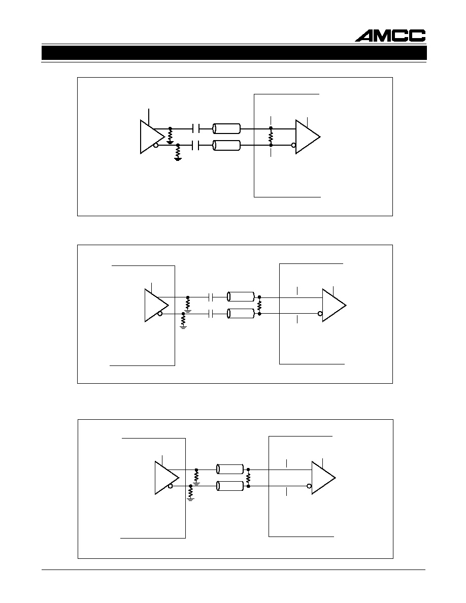
Figure 8. +5 V Differential PECL Driver to S2092 Input AC Coupled Termination
Figure 10. +3.3 V Differential LVPECL Driver to S2092 Reference Clock Input DC
Coupled Termination
Vcc -0.5 V
Vcc -0.5 V
S2092
REFCLKP/N
+3.3 V
100
150
150
+3.3 V
155 MHZ
OSCILLATOR/
155MCK from S3057
Zo=50
Zo=50
Figure 9. +5 V Differential PECL Driver to S2092 Reference Clock Input AC Coupled
Termination
Vcc -0.5 V
Vcc -0.5 V
S2092
REFCLKP/N
+5 V
100
330
330
+3.3 V
155 MHZ
OSCILLATOR
Zo=50
Zo=50
0.01
µ
F
0.01
µ
F

14
S2092
SERIAL BACKPLANE RETIMER DEVICE
July 10, 2000 / Revision A
CAP1
75
10
µ
F
CAP2
75
S2092
Figure 11. Loop Filter Capacitor Connections

15
S2092
SERIAL BACKPLANE RETIMER DEVICE
July 10, 2000 / Revision A
Ordering Information
X
I
F
E
R
P
E
C
I
V
E
D
E
G
A
K
C
A
P
t
i
u
c
r
i
C
d
e
t
a
r
g
e
t
n
I
≠
S
2
9
0
2
P
E
T
/
P
F
Q
T
n
i
P
8
4
≠
T
T
X
XXXX
XX
Prefix Device Package
AMCC is a registered trademark of Applied Micro Circuits Corporation.
Copyright Æ 2000 Applied Micro Circuits Corporation
D44/R111
AMCC reserves the right to make changes to its products or to discontinue any semiconductor product or service without notice, and
advises its customers to obtain the latest version of relevant information to verify, before placing orders, that the information being relied
on is current.
AMCC does not assume any liability arising out of the application or use of any product or circuit described herein, neither does it
convey any license under its patent rights nor the rights of others.
AMCC reserves the right to ship devices of higher grade in place of those of lower grade.
AMCC SEMICONDUCTOR PRODUCTS ARE NOT DESIGNED, INTENDED, AUTHORIZED, OR WARRANTED TO BE SUITABLE FOR
USE IN LIFE-SUPPORT APPLICATIONS, DEVICES OR SYSTEMS OR OTHER CRITICAL APPLICATIONS.
Applied Micro Circuits Corporation ∑ 6290 Sequence Dr., San Diego, CA 92121
Phone: (858) 450-9333 ∑ (800)755-2622 ∑ Fax: (858) 450-9885
http://www.amcc.com
C
E
R T I F I E
D
IS
O 9001