1
S2202
DUAL GIGABIT ETHERNET DEVICE
July 16, 1999 / Revision A
S2202
Æ
DUAL GIGABIT ETHERNET DEVICE
DEVICE
SPECIFICATION
MAC
(ASIC)
S2002
DUAL
GIGABIT
ETHERNET
INTERFACE
MAC
(ASIC)
TO SERIAL BACKPLANE
S2202
GE INTERFACE
SERIAL BP DRIVER
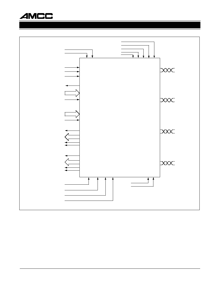
Figure 1. Typical Dual Gigabit Ethernet Application
FEATURES
∑ 1250 MHz (Gigabit Ethernet) operating rate
- Half rate operation
∑ Dual Transmitter with phase-locked loop (PLL)
clock synthesis from low speed reference
∑ Dual Receiver PLL provides clock and data
recovery
∑ Internally series terminated TTL outputs
∑ Low-jitter serial PECL interface
∑ Individual local loopback control
∑ JTAG 1149.1 Boundary scan on low speed I/O
signals
∑ Interfaces with coax, twinax, or fiber optics
∑ Single +3.3V supply, 1.85 W power dissipation
∑ Compact 21mm x 21mm 156 TBGA package
APPLICATIONS
∑ Ethernet Backbones
∑ Workstation
∑ Frame buffer
∑ Switched networks
∑ Data broadcast environments
∑ Proprietary extended backplanes
GENERAL DESCRIPTION
The S2202 facilitates high-speed serial transmission
of data in a variety of applications including Gigabit
Ethernet, serial backplanes, and proprietary point to
point links. The chip provides two separate trans-
ceivers which are operated individually for a data
capacity of >2 Gbps.
Each bi-directional channel provides parallel-to-se-
rial and serial-to-parallel conversion, clock genera-
tion/recovery, and framing. The on-chip transmit PLL
synthesizes the high-speed clock from a low-speed
reference. The on-chip dual receive PLL is used for
clock recovery and data re-timing on the two inde-
pendent data inputs. The transmitter and receiver
each support differential PECL-compatible I/O for
copper or fiber optic component interfaces with ex-
cellent signal integrity. Local loopback mode allows
for system diagnostics. The chip requires a 3.3V
power supply and dissipates 1.85 watts.
Figure 1 shows the S2202 and S2002 in a Gigabit
Ethernet application. Figure 2 summarizes the in-
put/output signals of the device. Figures 3 and 4
show the transmit and receive block diagrams, re-
spectively.

5
S2202
DUAL GIGABIT ETHERNET DEVICE
July 16, 1999 / Revision A
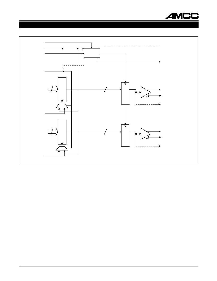
TRANSMITTER DESCRIPTION
The transmitter section of the S2202 contains a single
PLL which is used to generate the serial rate transmit
clock for all transmitters. Two channels are provided
with a variety of options regarding input clocking and
loopback. The transmitters operate at 1.250 GHz, 10
or 20 times the reference clock frequency.
Data Input
The S2202 has been designed to simplify the paral-
lel interface data transfer and provides the utmost in
flexibility regarding clocking of parallel data. The
S2202 incorporates a unique FIFO structure on both
the parallel inputs and the parallel outputs which en-
ables the user to provide a "clean" reference source
for the PLL and to accept a separate external clock
which is used exclusively to reliably clock data into
the device. Data can also be clocked in using the
REFCLK.
Data is input to each channel of the S2202 nominally
as a 10 bit wide word. An input FIFO and a clock
input, TBCx, are provided for each channel of the
S2202. The device can operate in two different
modes. The S2202 can be configured to use either
the TCLKx (TCLK MODE) input or the REFCLK input
(REFCLK MODE). In TCLK or REFCLK mode, 10
bits of data are clocked into its FIFO with the TBCx
provided with each 10 bits. Table 1 provides a sum-
mary of the input modes of the S2202.
Operation in the TBC MODE makes it easier for us-
ers to meet the relatively narrow setup and hold time
window required by the 125 Mbps 10-bit interface.
The TBC signal is used to clock the data into an
internal holding register and the S2202 synchronizes
its internal data flow to ensure stable operation.
However, regardless of the clock mode, REFCLK is
always the VCO reference clock. This facilitates the
provision of a clean reference clock resulting in mini-
mum jitter on the serial output. The TBC must be
frequency locked to REFCLK, but may have an arbi-
trary phase relationship. Adjustment of internal tim-
ing of the S2202 is performed during reset. Once
synchronized, the user must ensure that the timing
of the TBC signal does not change by more than
±
3
ns relative to the REFCLK.
Figure 5 demonstrates the flexibility afforded by the
S2202. A low jitter reference is provided directly to
the S2202 at either 1/10 or 1/20 the serial data rate.
This ensures minimum jitter in the synthesized clock
used for serial data transmission. A system clock
output at the parallel word rate, TCLKO, is derived
from the PLL and provided to the upstream circuit as
a system clock. The frequency of this output is con-
stant at the parallel word rate, 1/10 the serial data
rate, regardless of whether the reference is provided
at 1/10 or 1/20 the serial data rate. This clock can be
buffered as required without concern about added
delay. There is no phase requirement between
TCLKO and TBCx, which is provided back to the
S2202, other than that they remain within
±
3ns of
the phase relationship established at reset.
The S2202 also supports the traditional REFCLK
clocking found in many Gigabit Ethernet applications
and is illustrated in Figure 6.
Half Rate Operation
The S2202 supports full and half rate operation for
all modes of operation. When RATE is LOW, the
S2202 serial data rate equals the VCO frequency.
When RATE is HIGH, the VCO is divided by 2 before
being provided to the chip. Thus the S2202 can sup-
port Gigabit Ethernet and serial backplane functions
at both full and half the VCO rate. See Table 3.
Parallel to Serial Conversion
The 10-bit parallel data handled by the S2202 device
should be from a DC-balanced encoding scheme,
such as the 8B/10B transmission code, in which in-
formation to be transmitted is encoded, 8 bits at a
time, into a 10-bit transmission character and must
be compliant with IEEE 802.3z Gigabit Ethernet.
The 8B/10B transmission code includes serial en-
coding and decoding rules, special characters, and
error control. Information is encoded, 8 bits at a time,
into a 10 bit transmission character. The characters
defined by this code ensure that short run lengths
and enough transitions are present in the serial bit
stream to make clock recovery possible at the re-
ceiver. The encoding also greatly increases the like-
lihood of detecting any single or multiple errors that
might occur during the transmission and reception of
data
1
.
1. A.X. Widner and P.A. Franaszek, "A Byte-Oriented DC Bal-
anced (0,4) 8B/10B Transmission Code," IBM Research Report
RC9391, May 1982.
Table 1. Input Modes
E
D
O
M
T
n
o
i
t
a
r
e
p
O
0
a
t
a
d
k
c
o
l
c
o
t
d
e
s
u
K
L
C
F
E
R
.
e
d
o
M
K
L
C
F
E
R
.
s
l
e
n
n
a
h
c
ll
a
r
o
f
s
O
F
I
F
o
t
n
i
1
s
O
F
I
F
o
t
n
i
a
t
a
d
k
c
o
l
c
o
t
d
e
s
u
x
C
B
T
.
e
d
o
M
C
B
T
.
s
l
e
n
n
a
h
c
ll
a
r
o
f
Note that internal synchronization of FIFOs is performed upon
de-assertion of RESET.