 | –≠–ª–µ–∫—Ç—Ä–æ–Ω–Ω—ã–π –∫–æ–º–ø–æ–Ω–µ–Ω—Ç: S3006 | –°–∫–∞—á–∞—Ç—å:  PDF PDF  ZIP ZIP |
Applied Micro Circuits Corporation
6195 Lusk Blvd., San Diego, CA 92121 ∑ (619) 450-9333
1
S3005/S3006
SONET/SDH OC-3/12 TRANSMITTER AND RECEIVER
Æ
DEVICE SPECIFICATION
S3005/S3006
GENERAL DESCRIPTION
The S3005/S3006 Synchronous Electrical Transmit
Interface, SETI, and Synchronous Electrical Receive
Interface, SERI, SONET/SDH and E4 transmitter
and receiver chips are the first fully integrated serial-
ization/deserialization interface devices covering E4
(139.264 Mbit/s), SONET OC-3 (155.52 Mbit/s) and
SONET OC-12 (622.08 Mbit/s). With architecture de-
veloped by PMC-Sierra, the chipset performs all
necessary serial-to-parallel and parallel-to-serial
functions in conformance with SONET/SDH and E4
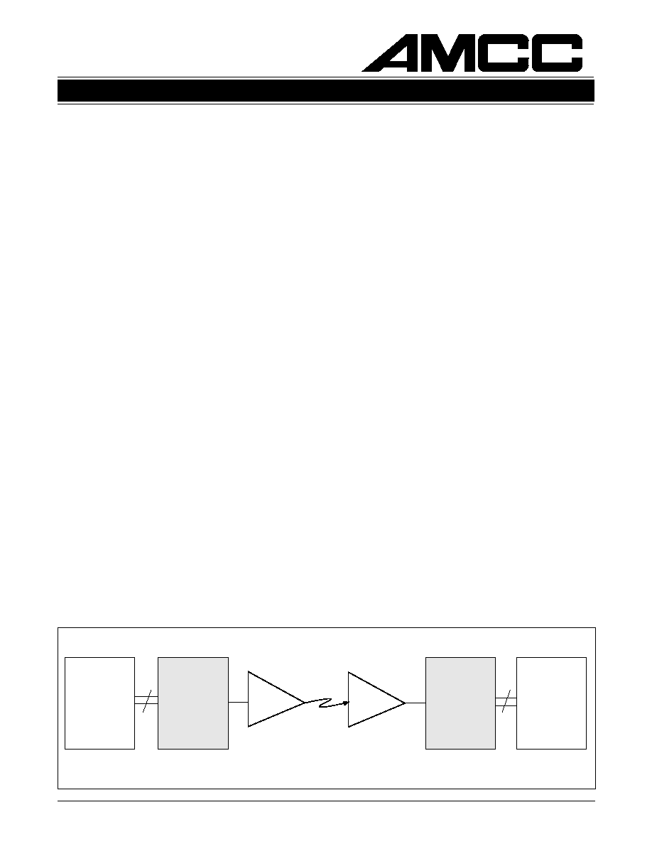
transmissions standards. Figure 1 shows a typical
network application.
On-chip clock synthesis is performed by the high-
frequency phase-locked loop on the S3005 SETI
transmitter chip allowing the use of a slower external
transmit clock reference. Clock recovery is per-
formed on the S3006 SERI receiver chip by
synchronizing its on-chip VCO directly to the incom-
ing data stream. The S3006 also performs SONET/
SDH frame detection. The chipset can be used with
19.44, 38.88, 51.84, and 77.76 MHz reference
clocks when operated in the SONET/SDH OC-3 or
OC-12 modes. In the E4 mode the chipset can be
operated with 17.408, 34.816, and 69.632 MHz ref-
erence clocks in support of existing system clocking
schemes. On-chip code-mark-inversion (CMI) encod-
ing and decoding is provided for 139.264 Mbit/s and
155.52 Mbit/s interfaces. If desired, both clock gen-
eration and recovery can be bypassed, allowing the
use of externally generated and recovered clocks.
The very low jitter ECL interface guarantees compli-
ance with the bit-error rate requirements of the
Bellcore, ANSI, and ITU-T standards. The S3005/
S3006 SETI and SERI chipset is packaged in a 50
mil pitch, 68-pin LDCC or 25 mil pitch, 80 PQFP
package, offering designers a small package outline.
FEATURES
∑ Complies with ANSI, Bellcore, and ITU-T
specifications
∑ On-chip high-frequency PLL for clock
generation and clock recovery
∑ Supports 139.264 Mbit/s (E4), 155.52 Mbit/s
(OC-3), and 622.08 Mbit/s (OC-12)
transmission rates
∑ Supports 139.264 Mbit/s and 155.52 Mbit/s
Code Mark Inversion (CMI) interfaces
∑ Selectable reference frequencies of 19.44,
38.88, 51.84, and 77.76 MHz (OC-3/12) and
17.408, 34.816, 46.421, and 69.632 MHz(E4)
∑ Interface to both ECL and TTL logic
∑ 8-bit TTL/CMOS datapath
∑ Bypass mode for off-chip clocking
∑ Local and line loopback mode
∑ Lock detect
∑ Low jitter ECL interface
∑ Low power
∑ 80 PQFP or 68 LDCC package
APPLICATIONS
∑ SONET/SDH or E4-based transmission systems
∑ SONET/SDH or E4 modules
∑ SONET/SDH or E4 test equipment
∑ ATM over SONET
∑ Section repeaters
∑ Add drop multiplexors
∑ Broadband cross-connects
∑ Fiber optic terminators
∑ Fiber optic test equipment
Figure 1. System Block Diagram
OTX
ORX
S3006
SONET/SDH
Receiver
(SERI)
Transmit
Overhead
Processor
Receive
Overhead
Processor
S3005
SONET/SDH
Transmitter
(SETI)
8
8
SONET/SDH OC-3/12 TRANSMITTER AND RECEIVER
Applied Micro Circuits Corporation
6195 Lusk Blvd., San Diego, CA 92121 ∑ (619) 450-9333
2
S3005/S3006
SONET/SDH OC-3/12 TRANSMITTER AND RECEIVER
Functions
Payload to
SPE mapping
Maintenance,
protection,
switching
Scrambling,
framing
Optical
transmission
Path layer
Line layer
Section layer
Photonic layer
Path layer
Line layer
Section layer
Photonic layer
End Equipment
End Equipment
Fiber Cable
Layer Overhead
(Embedded Ops
Channel)
576 Kbps
192 Kbps
0 bps
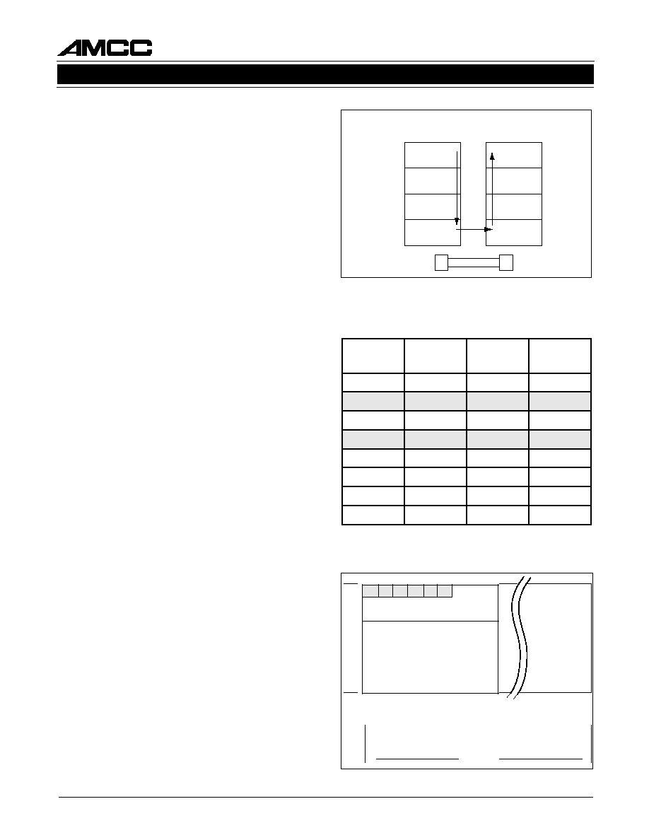
Figure 2. SONET Structure
Table 1. SONET Signal Hierarchy
9
Rows
9 x 261 =
2349 bytes
Transport Overhead
Synchronous Payload
Envelope
9 Columns
261 Columns
125
µ
sec
v
v
1
A
1
A
1
A
2
A
2
A
2
A
1
C
1
C
1
C
1
B
*
*
1
E
*
*
1
F
*
*
1
D
*
*
2
D
*
*
3
D
*
*
1
H
1
H
1
H
2
H
2
H
2
H
3
H
3
H
3
H
2
B
2
B
2
B
1
K
*
*
2
K
*
*
4
D
*
*
5
D
*
*
6
D
*
*
7
D
*
*
8
D
*
*
9
D
*
*
0
1
D
*
*
1
1
D
*
*
2
1
D
*
*
1
Z
1
Z
1
Z
2
Z
2
Z
2
Z
2
E
*
*
Figure 3. STS≠3/OC≠3 Frame Format
.
c
e
l
E
T
-
U
T
I
l
a
c
i
t
p
O
e
t
a
R
a
t
a
D
)
s
/
t
i
b
M
(
1
-
S
T
S
1
-
C
O
4
8
.
1
5
3
-
S
T
S
1
-
M
T
S
3
-
C
O
2
5
.
5
5
1
9
-
S
T
S
9
-
C
O
6
5
.
6
6
4
2
1
-
S
T
S
4
-
M
T
S
2
1
-
C
O
8
0
.
2
2
6
8
1
-
S
T
S
8
1
-
C
O
2
1
.
3
3
9
4
2
-
S
T
S
4
2
-
C
O
6
1
.
4
4
2
1
6
3
-
S
T
S
6
3
-
C
O
4
2
.
6
6
8
1
8
4
-
S
T
S
6
1
-
M
T
S
8
4
-
C
O
2
3
.
8
8
4
2
SONET OVERVIEW
Synchronous Optical Network (SONET) is a stan-
dard for connecting one fiber system to another at
the optical level. SONET, together with the Synchro-
nous Digital Hierarchy (SDH) administered by the
ITU-T, forms a single international standard for fiber
interconnect between telephone networks of differ-
ent countries. SONET is capable of accommodating
a variety of transmission rates and applications.
The SONET standard is a layered protocol with four
separate layers defined. These are:
∑ Photonic
∑ Section
∑ Line
∑ Path
Figure 2 shows the layers and their functions. Each
of the layers has overhead bandwidth dedicated to
administration and maintenance. The photonic layer
simply handles the conversion from electrical to optical
and back with no overhead. It is responsible for
transmitting the electrical signals in optical form over the
physical media. The section layer handles the transport
of the framed electrical signals across the optical
cable from one end to the next. Key functions of this
layer are framing, scrambling, and error monitoring.
The line layer is responsible for the reliable transmis-
sion of the path layer information stream carrying
voice, data, and video signals. Its main functions are
synchronization, multiplexing, and reliable transport.
The path layer is responsible for the actual transport
of services at the appropriate signaling rates.
Data Rates and Signal Hierarchy
Table 1 contains the data rates and signal designations
of the SONET hierarchy. The lowest level is the basic
SONET signal referred to as the synchronous transport
signal level-1 (STS-1). An STS-
N signal is made up of
N byte-interleaved STS-1 signals. The optical counter-
part of each STS-
N signal is an optical carrier level-N
signal (OC-
N). The S3005/S3006 chipset supports OC-3
rates (155.52 Mbit/s) and OC-12 (622.08 Mbit/s) rates.
Frame and Byte Boundary Detection
The SONET/SDH fundamental frame format for STS-3
consists of nine transport overhead bytes followed by
Synchronous Payload Envelope (SPE) bytes. This
pattern of 9 overhead and 261 SPE bytes is repeated
nine times in each frame. Frame and byte boundaries
are detected using the A1 and A2 bytes found in the
transport overhead. (See Figure 3)
For more details on SONET operations, refer to the
ANSI SONET standard document.

Applied Micro Circuits Corporation
6195 Lusk Blvd., San Diego, CA 92121 ∑ (619) 450-9333
3
S3005/S3006
SONET/SDH OC-3/12 TRANSMITTER AND RECEIVER
S3005/S3006 OVERVIEW
The S3005 SETI and S3006 SERI implement
SONET/SDH serialization/deserialization, transmission,
and frame detection/recovery functions. The block
diagrams in Figures 4 and 5 show basic operation of
both chips. These chips can be used to implement the
front end of SONET equipment, which consists primarily
of the serial transmit interface (S3005) and the serial
receive interface (S3006). The chipset handles all
the functions of these two elements, including paral-
lel-to-serial and serial-to-parallel conversion, clock
generation and recovery, and system timing, which
includes management of the datastream, framing, and
clock distribution throughout the front end.
Operation of the S3005/S3006 chips is straightfor-
ward. The sequence of operations is as follows:
Transmitter
1. 8-bit parallel input
2. Parallel-to-serial conversion
3. CMI encoding (optional)
4. Serial output
Figure 4. SONET/SDH Transmitter Functional Block Diagram
8
PIN[7:0]
8:1 PARALLEL
TO SERIAL
DLDP/N
TSDP/N
PICLK
TIMING
GEN
SYNC
PCLK
PAE
REFSEL[1:0]
CLOCK
SYNTHESIZER
LOCKDET
RSTB
D
2
2
TESTEN
BYTCLKIP
DLEB
CMI
MODE[2:0]
REFCLKP/N
2
3
LLEB
LLDP/N
LLCLKP/N
2
2
LOAD
DLCV
TSCLKP/N
2
Receiver
1. Clock and data recovery from serial input
2. CMI decoding (optional)
3. Frame detection
4. Serial-to-parallel conversion
5. 8-bit parallel output
Internal clocking and control functions are transpar-
ent to the user. Details of data timing can be seen in
Figures 10 through 18. On-chip clock generation can
be bypassed and an externally generated clock used
in its place, providing an additional measure of
design flexibility.
A lock detect feature is provided on both chips.
PMC PM5345
SUNI
Saturn User Network Interface
PMC PM5355
SUNI-622
Saturn User Network Interface
IGT WAC≠013≠A
SONET LAN ATM Processor
Fujitsu MB86683B NTC
Network Termination Controller
PMC PM5301
SSTX
Section Terminating Transceiver
PMC PM5312
STTX
Transport Terminating Transceiver
AT&T ASTROTEC1227/1230
650 Mbit/s
Fiber Optic Transmitter
Mitsubishi MF-622DF-T12-XXX
622 Mbit/s
Fiber Optic Transmitter
AT&T ASTROTEC 1310
650 Mbit/s
Fiber Optic Receiver
Mitsubishi MF-622DS-R1X-XXX 622 Mbit/s
Fiber Optic Receiver
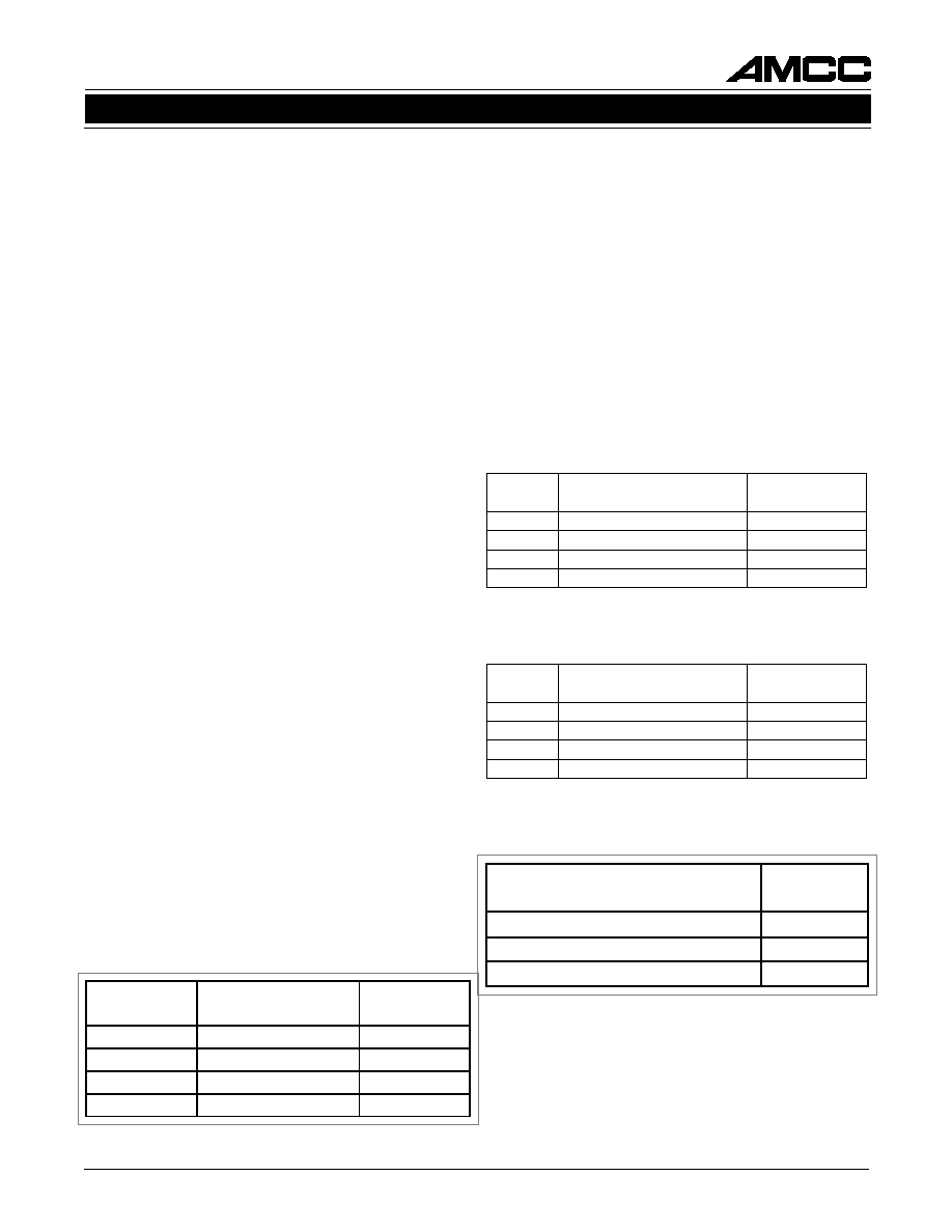
Suggested Interface Devices

Applied Micro Circuits Corporation
6195 Lusk Blvd., San Diego, CA 92121 ∑ (619) 450-9333
4
S3005/S3006
SONET/SDH OC-3/12 TRANSMITTER AND RECEIVER
For applications that provide a high-frequency bit
clock externally, the internal synthesizer may be by-
passed. Reference frequencies of 19.44 MHz, 38.88
MHz, 51.84 MHz, or 77.76 MHz are selectable for
SONET/SDH by the two reference select input pins.
In E4 applications, these same pins can select the
reference frequency from 17.408 MHz, 34.816 MHz,
46.421 MHz, or 69.632 MHz.
Loopback modes are provided for diagnostic
loopback (transmitter to receiver), or line loopback
(receiver to transmitter) when used with the compat-
ible S3006. (See Other Operating Modes.)
The operating mode is selected by three mode pro-
gramming inputs to be 622.08 Mbit/s, 155.52 Mbit/s,
155.52 Mbit/s with Coded-Mark-Inversion (CMI) en-
coding, or 139.264 Mbit/s with CMI encoding.
Figure 5. SONET/SDH Receiver Functional Block Diagram
1:8 SERIAL
TO PARALLEL
TIMING
GEN
M
U
X
BYTCLKIP
REFSEL[1:0]
CLOCK
RECOVERY
TESTEN
RSDP/N
DLDP/N
FRAME
BYTE
DETECT
DLEB
OOF
FP
POUT[7:0]
8
2
2
LOS
RSTB
TESTRST
BACKUP
REFERENCE
GEN
POCLK
LOCKDET
C
M
I
LCV
LLCLKP/N
LLDP/N
2
2
2
REFCLKP/N
2
MODE[2:0]
3
S3005 TRANSMITTER FUNCTIONAL
DESCRIPTION
The S3005 SETI transmitter chip performs the serial-
izing stage in the processing of a transmit SONET
STS-12, STS-3, or ITU-T E4 bit serial data stream. It
converts the byte serial data stream to bit serial for-
mat at 622.08, 155.52, or 139.264 Mbit/s depending
on the control settings and reference frequency pro-
vided by the user. A Coded-Mark-Inversion (CMI) is
available for use during 155.52 Mbit/s STS-3 (electri-
cal) and 139.264 Mbit/s E4 operational modes. (See
Other Operating Modes.)
A high-frequency bit clock can be generated from a
variety of lower frequency references by using the
integral frequency synthesizer consisting of a phase-
locked loop circuit with an adjustable divider in the loop.
Applied Micro Circuits Corporation
6195 Lusk Blvd., San Diego, CA 92121 ∑ (619) 450-9333
5
S3005/S3006
SONET/SDH OC-3/12 TRANSMITTER AND RECEIVER
Clock Synthesizer
The Clock Synthesizer, shown in the block diagram
in Figure 4, is a monolithic PLL that generates the
serial output clock phase synchronized with the input
reference clock (REFCLK). There are three select-
able output clock frequencies that are synthesizable
from any of four selectable reference frequencies for
SONET/SDH operation.
The MODE[2:0] inputs select the output serial clock
frequency to be 622.08 MHz for STS-12, 311.04
MHz for CMI-encoded STS-3, 155.52 MHz for STS-
3, or 278.528 MHz for CMI-encoded E4. Their
frequencies are selected as shown in Table 2.
The REFSEL[1:0] inputs in combination with the
MODE[2:0] inputs select the ratio between the out-
put clock frequency and the reference input
frequency, as shown in Tables 3 and 4. This ratio is
adjusted for each of the four modes so that the refer-
ence frequency selected by the REFSEL[1:0] is the
same for all modes.
The REFCLK input must be generated from a differ-
ential ECL crystal oscillator which has a frequency
accuracy of better than 20 ppm in order for the
TSCLK frequency to have the same accuracy re-
quired for operation in a SONET system.
In order to meet the .01 UI SONET jitter specifications,
the maximum reference clock jitter must be guaran-
teed over the 12KHz to 1MHz bandwidth. For details
of reference clock jitter requirements, see Table 5.
The on≠chip PLL consists of a phase detector, which
compares the phase relationship between the VCO
output and the REFCLK input, a loop filter which
converts the phase detector output into a smooth DC
voltage, and a VCO, whose frequency is varied by
this voltage.
The loop filter generates a VCO control voltage based
on the average DC level of the phase discriminator
output pulses. The loop filter's corner frequency is
optimized to minimize output phase jitter. The loop
filter capacitor is included on the package.
Timing Generator
The Timing Generator function, seen in Figure 4, pro-
vides two separate functions. It provides a byte rate
version of the TSCLK, and a mechanism for aligning
the phase between the incoming byte clock and the
clock which loads the parallel-to-serial shift register.
The PCLK output is a byte rate version of TSCLK.
For STS-12, the PCLK frequency is 77.76 MHz, and
for NRZ or CMI coded STS-3, its frequency is 19.44
MHz. For CMI coded E4, its frequency is 17.408
MHz. PCLK is intended for use as a byte speed clock
for upstream multiplexing and overhead processing
circuits. Using PCLK for upstream circuits will ensure
a stable frequency and phase relationship between
the data coming into and leaving the S3005 device.
MODE[2:0]
OUTPUT CLOCK
FREQUENCY
OPERATING
MODE
100
622.08 MHz
STS≠12
001
311.04 MHz
STS≠3 CMI
010
155.52 MHz
STS≠3
011
278.528 MHz
E4 CMI
Table 2. Clock Frequency Options
Table 3. Reference Frequency Options
Table 4. E4CMI Reference Frequency Options
Table 5. Reference Jitter Limits
Maximum Reference Clock Jitter
in 12 KHz to 1 MHz Band
Operating
Mode
14 ps
STS≠12
28 ps
STS≠3 CMI
56 ps
STS≠3
L
E
S
F
E
R
]
0
:
1
[
]
0
:
1
[
]
0
:
1
[
]
0
:
1
[
]
0
:
1
[
K
C
O
L
C
E
C
N
E
R
E
F
E
R
Y
C
N
E
U
Q
E
R
F
Y
C
N
E
U
Q
E
R
F
Y
C
N
E
U
Q
E
R
F
Y
C
N
E
U
Q
E
R
F
Y
C
N
E
U
Q
E
R
F
G
N
I
T
A
R
E
P
O
E
D
O
M
E
D
O
M
E
D
O
M
E
D
O
M
E
D
O
M
0
0
z
H
M
4
4
.
9
1
3
≠
S
T
S
,
2
1
≠
S
T
S
1
0
z
H
M
8
8
.
8
3
3
≠
S
T
S
,
2
1
≠
S
T
S
0
1
z
H
M
4
8
.
1
5
3
≠
S
T
S
,
2
1
≠
S
T
S
1
1
z
H
M
6
7
.
7
7
2
1
≠
S
T
S
L
E
S
F
E
R
]
0
:
1
[
]
0
:
1
[
]
0
:
1
[
]
0
:
1
[
]
0
:
1
[
K
C
O
L
C
E
C
N
E
R
E
F
E
R
Y
C
N
E
U
Q
E
R
F
Y
C
N
E
U
Q
E
R
F
Y
C
N
E
U
Q
E
R
F
Y
C
N
E
U
Q
E
R
F
Y
C
N
E
U
Q
E
R
F
G
N
I
T
A
R
E
P
O
E
D
O
M
E
D
O
M
E
D
O
M
E
D
O
M
E
D
O
M
0
0
z
H
M
8
0
4
.
7
1
--
1
0
z
H
M
6
1
8
.
4
3
--
0
1
z
H
M
1
2
4
.
6
4
--
1
1
z
H
M
2
3
6
.
9
6
--