 | –≠–ª–µ–∫—Ç—Ä–æ–Ω–Ω—ã–π –∫–æ–º–ø–æ–Ω–µ–Ω—Ç: S3015 | –°–∫–∞—á–∞—Ç—å:  PDF PDF  ZIP ZIP |
E4/STM-1/OC-3 ATM INTERFACE CIRCUITS
S3015/S3016
1
E4/STM-1/OC-3 ATM INTERFACE CIRCUITS
S3015/S3016
FEATURES
∑ Complies with ANSI, Bellcore, and ITU-T
specifications
∑ On-chip high-frequency PLL for clock
generation and clock recovery
∑ On-chip analog circuitry for transformer driver
and equalization
∑ Supports 139.264 Mbit/s (E4) and 155.52 Mbit/s
(OC-3) transmission rates
∑ Supports 139.264 Mbit/s and 155.52 Mbit/s
Coded Mark Inversion (CMI) interfaces
∑ Reference frequencies of 19.44 (OC-3) or
17.408 MHz (E4)
∑ Interface to both PECL and TTL logic
∑ Lock detect on clock recovery device
∑ Low jitter PECL interface
∑ 1.6W total typ power
∑ +5V only power supply
∑ Small 52 PQFP TEP package
∑ Supports both electrical and optical interfaces
APPLICATIONS
∑
ATM over SONET
∑
OC-3/STM-1 or E4-based transmission systems
∑
OC-3/STM-1 or E4 modules
∑
OC-3/STM-1 or E4 test equipment
∑
Section repeaters
∑
Add drop multiplexors
∑
Broadband cross-connects
∑ Fiber optic terminators
∑ Fiber optic test equipment
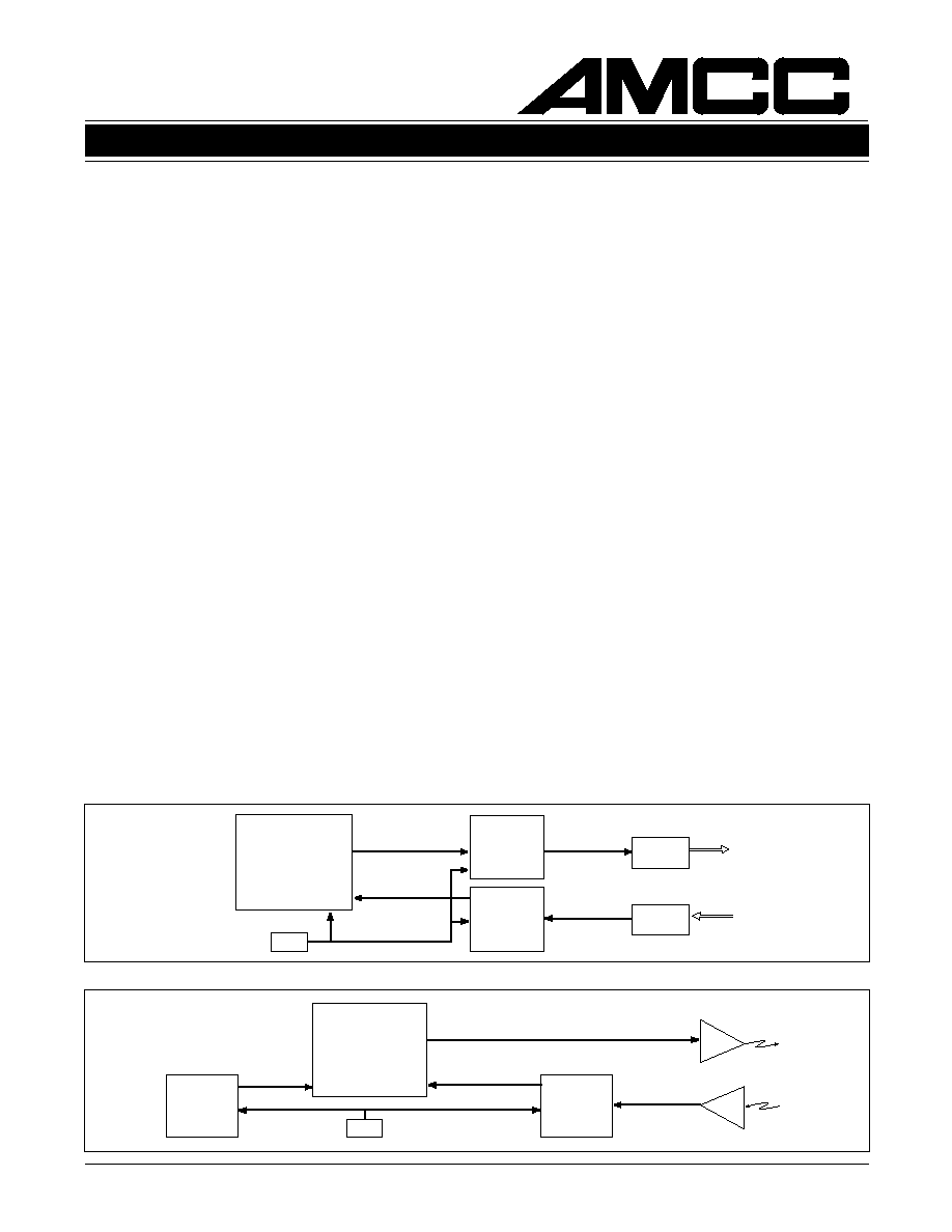
GENERAL DESCRIPTION
The S3015 transmitter and S3016 receiver derive high
speed timing signals for SONET/SDH or PDH≠based
equipment. These circuits are implemented using
AMCC's proven Phase Locked Loop (PLL) technology.
Figures 1a and 1b show typical network applications.
The S3015 and S3016 each have an on-chip VCO
which can be synchronized directly to the incoming data
stream. The chipset can be used with a 19.44 MHz
reference clock when operated in the SONET/SDH OC-
3 mode. In E4 mode the chipset can be operated with a
17.408 MHz reference clock in support of existing
system clocking schemes. On-chip coded-mark-inver-
sion (CMI) encoding and decoding is provided for
139.264 Mbit/s and 155.52 Mbit/s interfaces.
The low jitter PECL interface guarantees compliance
with the bit-error rate requirements of the Bellcore,
ANSI, and ITU-T standards. The S3015/S3016 chipset
is packaged in a .65mm pitch, compact 52-pin PQFP,
offering designers a small package outline.
The S3015 and S3016 provide the major components
on-chip for a coaxial cable interface, including analog
transformer driver circuitry and equalization interface
circuitry.
Figure 1a. Electrical Interface
Figure 1b. Optical Interface
E4/STM-1/OC-3
OVERHEAD
PROCESSOR
OSC
S3016
S3015
XFMR
139/155 Mb/s NRZ
139/155 Mb/s CMI
COAX
139/155 Mb/s NRZ
139/155 Mb/s CMI
17.408/19.44 Mhz
XFMR
COAX
E4/STM-1/OC-3
OVERHEAD
PROCESSOR
OSC
S3016
S3015
155 MHz
155 Mb/s NRZ
155 Mb/s NRZ
155 Mb/s NRZ
OTX
ORX
DEVICE SPECIFICATION
Æ
2
S3015/S3016
E4/STM-1/OC-3 ATM INTERFACE CIRCUITS
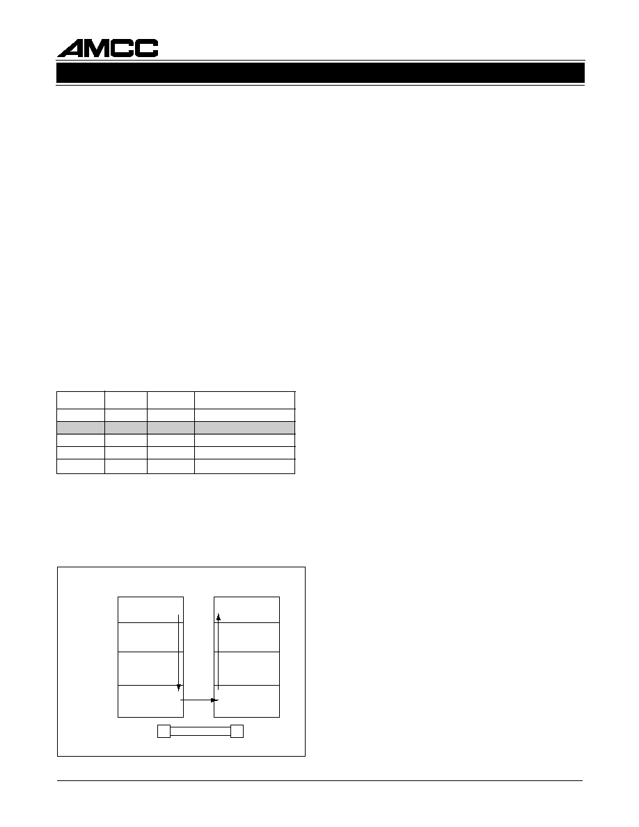
SONET/SDH OVERVIEW
Synchronous Optical Network (SONET) is a standard
for connecting one fiber system to another at the optical
level. SONET, together with the Synchronous Digital
Hierarchy (SDH) administered by the ITU-T, form a
single international standard for fiber interconnect be-
tween telephone networks of different countries. SONET
is capable of accommodating a variety of transmission
rates and applications.
The SONET standard is a layered protocol with four
separate layers defined. These are:
∑ Photonic
∑ Section
∑ Line
∑ Path
Figure 2 shows the layers and their functions. Each of
the layers has overhead bandwidth dedicated to admin-
istration and maintenance. The photonic layer simply
handles the conversion from electrical to optical and
back with no overhead. It is responsible for transmitting
the electrical signals in optical form over the physical
media. The section layer handles the transport of the
framed electrical signals across the optical cable from
one end to the next. Key functions of this layer are
framing, scrambling, and error monitoring. The line
layer is responsible for the reliable transmission of the
path layer information stream carrying voice, data, and
video signals. Its main functions are synchronization,
multiplexing, and reliable transport. The path layer is
responsible for the actual transport of services at the
appropriate signaling rates.
Data Rates and Signal Hierarchy
Table 1 contains the data rates and signal designations
of the SONET hierarchy. The lowest level is the basic
SONET signal referred to as the synchronous transport
signal level-1 (STS-1). An STS-
N signal is made up of
N byte-interleaved STS-1 signals. The optical counter-
part of each STS-
N signal is an optical carrier level-N
signal (OC-
N). The S3015/S3016 chipset supports OC-
3 rates (155.52 Mbit/s).
Frame and Byte Boundary Detection
The SONET/SDH fundamental frame format for STS-3
consists of nine transport overhead bytes followed by
Synchronous Payload Envelope (SPE) bytes. This pat-
tern of 9 overhead and 261 SPE bytes is repeated
nine times in each frame. Frame and byte boundaries
are detected using the A1 and A2 bytes found in the
transport overhead. (See Figure 3.)
For more details on SONET operations, refer to the
ANSI SONET standard document.
Elec.
ITU-T
Optical Data Rate (Mbit/s)
STS-1
OC-1
51.84
STS-3
STM-1
OC-3
155.52
STS-12
STM-4
OC-12
622.08
STS-24
OC-24
1244.16
STS-48
STM-16
OC-48
2488.32
Table 1. SONET Signal Hierarchy
Figure 3. SONET Structure
End Equipment
Payload to
SPE mapping
Maintenance,
protection,
switching
Optical
transmission
Scrambling,
framing
Fiber Cable
End Equipment
Section layer
Photonic layer
Line layer
Path layer
Path layer
Section layer
Photonic layer
Line layer
Functions
Transport Overhead
9 Columns
Synchronous
Payload
Envelope
125
µ
sec
9 x 261 =
2349 bytes
9
Rows
Figure 3. STS-3 Frame Format
E4/STM-1/OC-3 ATM INTERFACE CIRCUITS
S3015/S3016
3
S3015 TRANSMITTER
FUNCTIONAL DESCRIPTION
The S3015 transmitter chip performs the last stage of
digital processing of a transmit SONET STS-3 or ITU-
T E4 bit serial data stream. A Coded Mark Inversion
(CMI) encoder can be enabled for encoding STS-3
electrical and E4 signals.
Clock Recovery
If serial data is present on the SERDATIP/N inputs, the
clock is recovered from the serial data stream at 139.264
MHz or 155.52 MHz and synthesized to 278.528 MHz
or 311.04 MHz to CMI encode the incoming data.
Optical and Electrical Interfaces
The digital data outputs (SERDATOP/N) are the PECL
outputs for an optical interface and are to be connected
to an electrical to optical converter, as shown in Figure
18. This data is also routed to two on-chip transformer
drivers and sent out on XFRMDRVA and XFRMDRVB
to drive the transformers of the electrical interface, as
shown in Figure 20. These outputs are shut off when the
reset is active, XFRMEN is active, or when the chip is
in NRZ mode and the data inputs are in the logic zero
state. The electrical characteristics for the transformer
drivers are shown in Table 5.
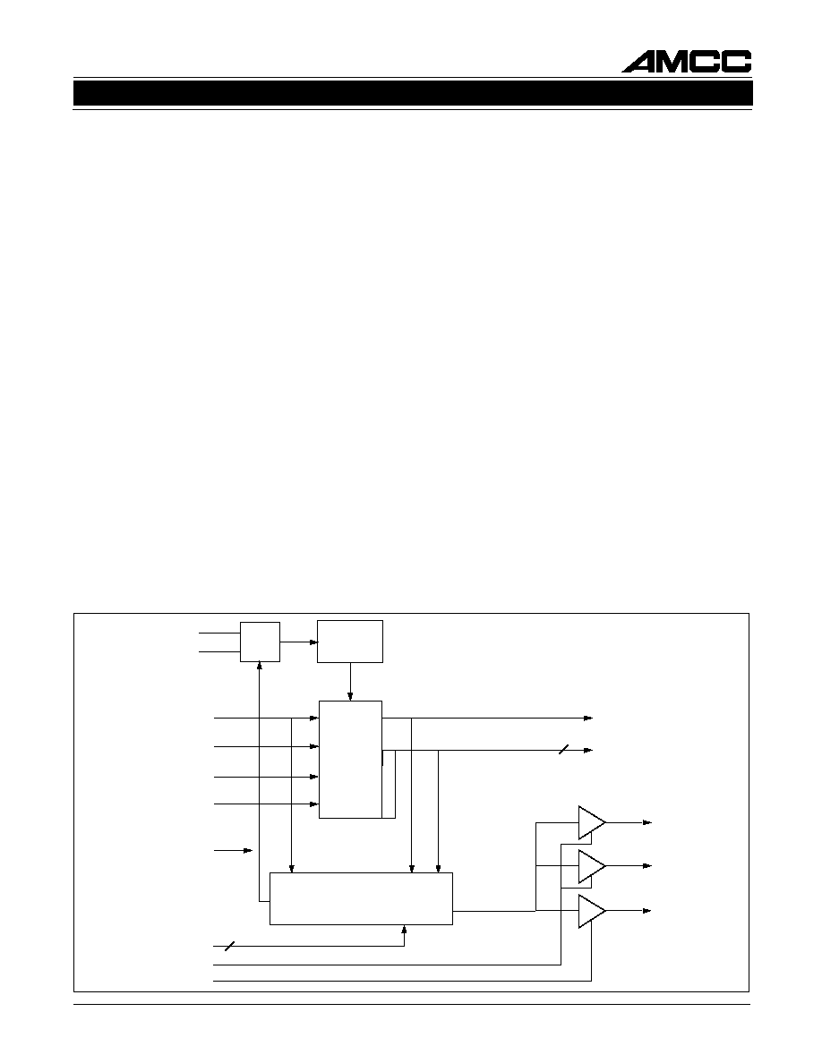
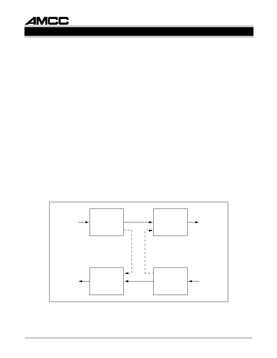
S3015/S3016 OVERVIEW
The S3015 transmitter and the S3016 receiver can be
used to implement the front end of STS-3, OC-3 or E4
equipment. The block diagrams in Figures 4 and 10
show the basic operation of both chips.
When serial data is present at the input of the transmitter,
the S3015 VCO synchronizes directly to the incoming data,
which is retimed for the purpose of optional CMI encod-
ing. In the absence of incoming serial data, the S3015
operates as a clock synthesizer. In this mode, a crystal
oscillator is connected to the TTL reference input and
synthesized up to the 155 MHz output frequency. The
S3016 receiver performs clock recovery by synchroniz-
ing its on-chip VCO directly to the incoming data stream.
The S3015 provides a PECL output for an optical
interface and two transformer driver outputs for an
electrical interface. One of these drivers is a monitor
output. The S3016 provides a PECL input for an optical
interface and an analog input for an electrical interface.
When the chipset is used in an electrical interface, the
PECL output of the transmitter can be connected to the
PECL input of the receiver to implement a diagnostic
loopback mode for test. When the chipset is used in an
optical interface, a transformer driver output of the
transmitter can be connected to the analog input of the
receiver to implement the loopback mode.
Figure 4. S3015 OC3/STM-1/E4 Transmitter Functional Block Diagram
2
2
SERCLKOP/N
REFCKOUT
SERDATOP/N
XFRMEN
SERDATEN
XFRMDRVB
XFRMDRVA
TRANSFORMER
DRIVERS
REFCKIN
TSTCLKEN
CMISEL
DLCV
RSTB
SERDATIP/N
LOOP
FILTER
VCO
CLOCK
DIVIDER
PHASE DETECTOR
CAP1
CAP2
C
M
I
4
S3015/S3016
E4/STM-1/OC-3 ATM INTERFACE CIRCUITS
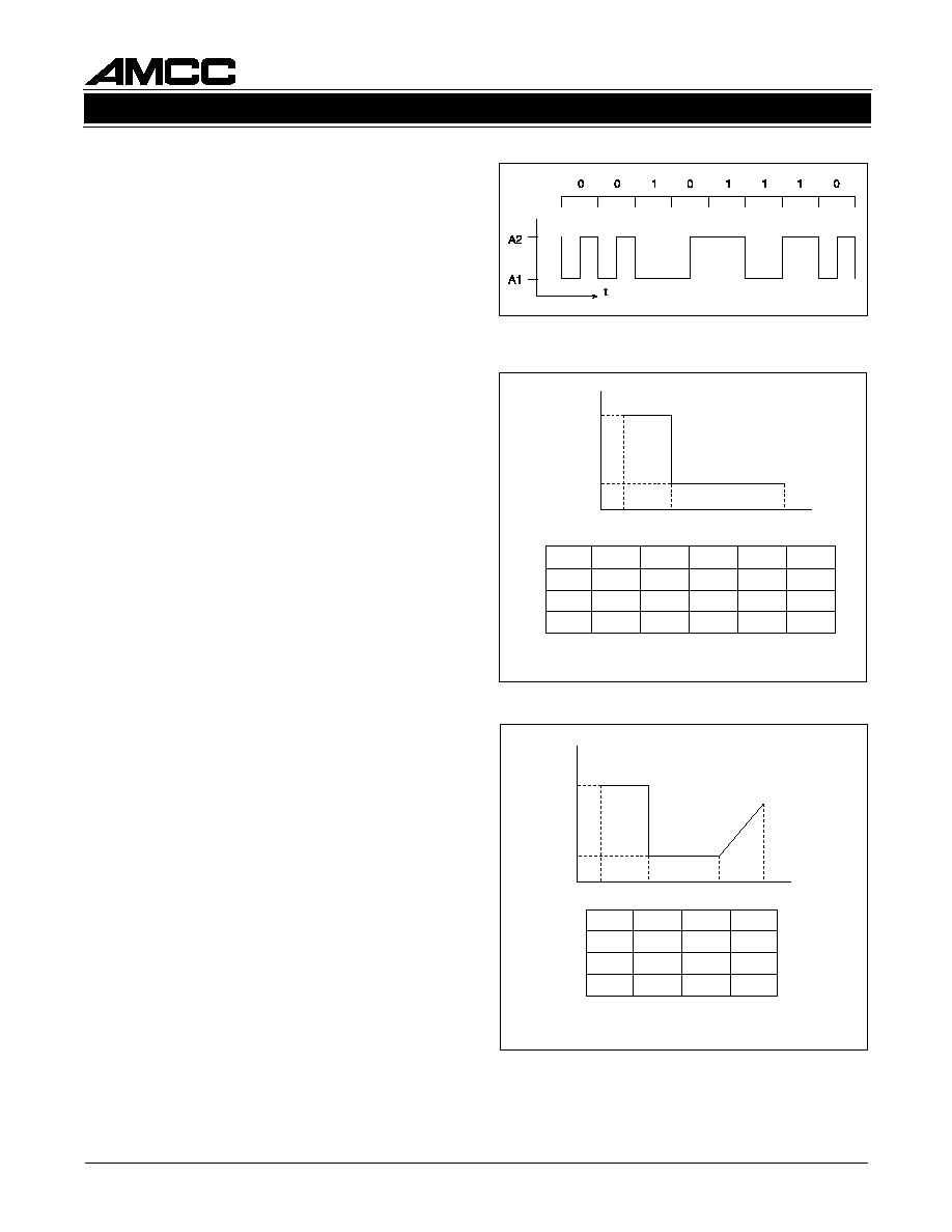
CMI Encoding
Coded Mark Inversion format (CMI) ensures at least
one data transition per 1.5 bit periods, thus aiding
the clock recovery process. Zeros are represented
by a Low state for one half a bit period, followed by
a High state for the rest of that bit period. Ones are
represented by a steady Low or High state for a full
bit period. The state of the ones bit period alternates
at each occurrence of a one. Figure 5 shows an
example of CMI-encoded data. The STS-3 electrical
interface and the E4 interface are specified to have
CMI-encoded data.
The CMI encoder on the S3015 accepts serial data
from SERDATIP/N at 139.264 or 155.52 Mb/s. The
data is then encoded into CMI format, and the result
is shifted out with transitions at twice the basic data
rate. The CMISEL input controls whether the CMI en-
coder is in the data path. A CMI code violation can be
inserted for diagnostic purposes by activating the
DLCV input. The DLCV input is sampled on every
cycle of the serial clock to allow a single or multiple
line code violations to be inserted. This violation is
either an inverted zero code or an inversion of the
alternating ones logic level, depending on the state of
the data. Subsequent one codes take into account
the induced violation to avoid error multiplication.
Jitter Generation
Jitter Generation is defined as the amount of jitter at the
OC-3 or E-4 output of equipment. Jitter generation for
OC-3 shall not exceed 0.01 UI rms when measured
using a highpass filter with a 12 kHz cutoff frequency.
For STM-1 and E4, the jitter generated shall not exceed
the specifications shown in Figure 6.
In order to meet the SONET, STM-1 E4 jitter specifica-
tions as shown in Figure 6, the SERDATIP/N serial data
input must meet the jitter characteristics as shown in
Figure 7.
Figure 6. Jitter Generation Specifications
Compliant to G.823 and G.825
Figure 7. S3015 Maximum Allowable Input Jitter
f1
STM-1
500
f1(Hz)
E4
1. UI rms
2. UI p≠p
200
65
f2(KHz)
10
1.3
f3(MHz)
3.5
1.5
(2)
A1
1.5
(2)
.15
(2)
OC-3
--
--
--
.01
(1)
.01
(1)
A2
.075
(2)
A1
A2
f2
f3
500Hz
STM-1
65
f2(KHz)
E4
10
1. UI rms
2. UI p≠p
1.45
(2)
A1
1.45
(2)
.10
(2)
OC-3
--
.005
(1)
.005
(1)
A2
.025
(2)
A1
A2
f2
1.3 MHz
225 KHz
Slope = +20 dB/decade
Figure 5. CMI Encoded Data

E4/STM-1/OC-3 ATM INTERFACE CIRCUITS
S3015/S3016
5
Figure 8. Mask of a pulse corresponding to a binary 0 Compliant to G.703
Notes:
1. The maximum "steady state" amplitude should not exceed the 0.55 V limit. Overshoots and other transients are
permitted to fall into the dotted area, bounded by the amplitude levels 0.55 V and 0.6 V, provided that they do not
exceed the steady state level by more than 0.05 V. The possibility of relaxing the amount by which the overshoot may
exceed the steady state level is under study.
2. For the purpose of these masks, the rise time and decay time should be measured between -0.4 V and 0.4 V, and
should not exceed 2 ns.
3. The inverse pulse in Figure 9 will have the same characteristics, noting that the timing tolerances at the zero level of the
negative and positive transitions are
±
0.1 ns and
±
0.5 ns respectively.
Figure 9. Mask of a pulse corresponding to a binary 1 Compliant to G.703
T=
7.18 ns for E4
6.43 ns for 155 CMI
T=
7.18 ns for E4
6.43 ns for 155 CMI
t=
1.35 ns for E4
1.20 ns for 155 CMI

6
S3015/S3016
E4/STM-1/OC-3 ATM INTERFACE CIRCUITS
S3016 RECEIVER FUNCTIONAL
DESCRIPTION
The S3016 receiver provides the first stage of digital
processing of a receive SONET STS-3 or ITU-T E4 serial
bit stream. A Coded Mark Inversion (CMI) decoder can
be enabled for decoding STS-3 electrical and E4 signals.
Clock recovery is performed on the incoming
scrambled NRZ or CMI≠coded data stream. A reference
clock is required for phase locked loop start-up and
proper operation under loss of signal conditions. An
integral prescaler and phase locked loop circuit is used
to multiply this reference frequency to the nominal bit rate.
Clock Recovery
The Clock Recovery function, as shown in the block
diagram in Figure 10, generates a clock that is fre-
quency matched to the incoming data baud rate at
the SERDATIP/N differential inputs. The clock is
phase aligned by a PLL so that it samples the data
in the center of the data eye pattern.
The phase relationship between the edge transitions
of the data and those of the generated clock are
compared by a phase/frequency discriminator. Output
pulses from the discriminator indicate the required
direction of phase corrections. These pulses are
smoothed by an integral loop filter. The output of the
loop filter controls the frequency of the Voltage Con-
trolled Oscillator (VCO), which generates the recov-
ered clock. Frequency stability without incoming data
is guaranteed by an alternate reference input
(REFCKIN) to which the PLL locks when data is lost.
When the test clock enable (TSTCLKEN) input is set
high, the clock recovery block is disabled. The refer-
ence clock (REFCKIN) is used as the bit rate clock
input in place of the recovered clock. This feature is
used for functional testing of the device.
The loop filter transfer function is optimized to enable
the PLL to track the jitter, yet tolerate the minimum
transition density expected in a received SONET or
E4 data signal. This transfer function yields a typical
capture time of 16
µ
s for random incoming NRZ data.
The total loop dynamics of the clock recovery PLL yield
a jitter tolerance which exceeds the minimum tolerance
proposed for OC-3/STM-1/E4 equipment by the Bellcore
and ITU-T documents, shown in Figure 13.
Optical and Electrical Interfaces
The digital data inputs (SERDATIP/N) are the PECL
inputs from an optical to electrical converter, as shown
in Figure 16. The data input for the coaxial interface is
ANDATIN, which is the serial data input from the equal-
izer circuit and should be connected as shown in Figure
17. The EQUALSEL input is used to select either
SERDATIP/N or ANDATIN.
2
2
2
2
SERCLKOP/N
REFCKOUT
LCV
LOSOUT
SERDATOP/N
REFCKIN
TSTCLKEN
CMISEL
RSTB
EQUALSEL
LOSIN
LOSREF
LOSOPT
ANDATIN
C
M
I
SERDATIP/N
LOOP
FILTER
VCO
CLOCK
DIVIDER
PHASE DETECTOR
LOCK
DETECTOR
CAP1
CAP2
BUFINA, BUFINB
BUFOUT
2:1
MUX
2:1
MUX
Figure 10. S3016 OC-3/STM-1/E4 Receiver Functional Block Diagram

E4/STM-1/OC-3 ATM INTERFACE CIRCUITS
S3015/S3016
7
CMI Decoding
The CMI decoder block on the S3016 accepts serial
data from the SERDATIP/N input at the rate of 139.264
or 155.52 Mb/s. The incoming CMI data, which has
transitions that represent this data rate (the clock asso-
ciated with this data would be running at twice this rate),
is then decoded from CMI to NRZ format.
Loss of Signal
The clock recovery circuit monitors the incoming data
stream for loss of signal. If the incoming encoded data
stream has had no transitions continuously for 96 to 224
recovered clock cycles, loss of signal is declared and
the PLL will switch from locking onto the incoming data
to locking onto the reference clock per the requirements
of G.775. Alternatively, the loss-of signal (LOSIN) input
can force a loss-of-signal condition. This signal is com-
pared internally against the LOSREF input reference
voltage. This input can be set to meet the conditions
shown in Figure 11. If the zero to peak signal level drops
below the LOSREF/20 voltage level for more than 96 to
224 bit intervals, a loss of signal condition will be
indicated on the LOSOUT pin and the PLL will change
its reference from the serial data stream to the reference
clock. When the peak input voltage is greater than
LOSREF/10, the loss of signal condition will be
deasserted and the PLL will recover the clock from the
serial data inputs.
In NRZ mode, a logic low level on the LOSOPT input will
cause the PLL to change its reference to the reference
clock. This pin should be driven by a PECL compatible
level signal detect signal from the fiber optic receiver.
Serial Clock Output to Data Output Timing
The serial data is clocked out on the falling edge of
SERCLKOP. (See Figure 12.) This timing is valid in
both NRZ and CMI modes.
Input Jitter Tolerance
Input jitter tolerance is defined as the peak to peak
amplitude of sinusoidal jitter applied on the input signal
that causes an equivalent 1 dB optical/electrical power
penalty. OC-3 and E-4 input jitter tolerance require-
ments are shown in Figure 13.
The S3016 PLL complies with the minimum jitter toler-
ance for clock recovery proposed for SONET/SDH
equipment defined by the Bellcore TA-NWT-000253
standard when used as shown in Figure 13. The S3016
PLL also complies with the minimum jitter tolerance for
clock recovery as defined in the ITU-T E4 specification
when used as shown in Figure 17.
f9
OC-3
10
f9
(Hz)
E4
TBD
30
f0
(Hz)
TBD
300
f1
(Hz)
200
6.5
f2
(KHz)
0.5
65
f3
(KHz)
65
--
f4
(MHz)
1.3
15
A2
15
1.5
A3
1.5
.15
STM-1 (Optical) 0.125 19.3
500
6.5
65
1.3
39
1
1.5 0.15
STM-1 (Electrical) 0.125 19.3
500
3.25
65
1.3
39
1
1.5 0.075
A4
0.075
A2
A3
A4
f0
f1
f2
f3
f4
Sinusoidal
Input Jitter
Amplitude
(UI p-p)
Figure 13. Clock Recovery Jitter Tolerance
Compliant to G.823 and G.825
maximum
cable loss
nominal value
Tolerance range
"no transition condition" or "transition
condition" may be declared
"transition condition"
must be declared
"no transition condition"
must be declared
Level below Nominal
The signal level 17 is (maximum cable loss +3)
dB below nominal.
3 dB
The signal level 35 is greater than the maximum
expected cross-talk level.
17
35
Figure 11. Criteria for determination of transition
conditions. Compliant to G.775.
Note:
1. Only tested to 20 due to test equipment limitation.
SERCLKOP
SERDATOP/N
tPSER
Figure 12. S3016 Clock to Data Timing
8
S3015/S3016
E4/STM-1/OC-3 ATM INTERFACE CIRCUITS
Figure 14. Loopback Diagram
S3015
S3016
S3015
S3016
Control
CLK
Diagnostic
Loopback
Diagnostic
Loopback
CLK
Control
Reference Clock Input
The reference clock input seen in Figure 10 provides
backup reference clock signals to the clock recovery
block when the clock recovery block detects a loss of
signal condition. It contains a counter that divides the
clock output from the clock recovery block down to the
same frequency as the reference clock REFCKIN.
OTHER OPERATING MODES
Diagnostic Loopback
When the chipset is used in an electrical interface, the
serial data output (SERDATOP/N) of the transmitter
can be connected the serial data input (SERDATIP/N)
of the receiver to implement a loopback test for diagnos-
tic purposes, as shown in Figure 14. In this mode,
SERDATEN on the transmitter and EQUALSEL on the
receiver are both held low. LOSOPT on the receiver is
held high or not connected.
Test Mode
The Test Clock Enable (TSTCLKEN) inputs on both
chips provide access to the PLL.
The PLL-generated clock source on both the S3015
and S3016 can be bypassed by setting TSTCLKEN
high. In this mode, an externally generated clock source
must be applied at the REFCLKIN input.
Clock Synthesis
In the Clock Synthesis mode, the S3015 synthesizes
the E4 (139.264 MHz) clock from a 17.408 MHz crystal
oscillator or the STS-3/STM-1 (155.52 MHz) clock from
a 19.44 MHz crystal oscillator. In this mode, a crystal
oscillator is connected to the TTL reference input and
synthesized up to the output frequency.
The S3015 PLL complies with jitter generation for clock
synthesis proposed for SONET/SDH equipment de-
fined by the Bellcore TA-NWT-000253 standard, when
used with a crystal reference source as defined in Table 4.

E4/STM-1/OC-3 ATM INTERFACE CIRCUITS
S3015/S3016
9
S3015 Pin Assignment and Descriptions
e
m
a
N
n
i
P
l
e
v
e
L
O
/
I
#
n
i
P
n
o
i
t
p
i
r
c
s
e
D
N
I
K
C
F
E
R
L
T
T
I
0
1
t
i
b
l
a
n
r
e
t
n
i
e
h
t
r
o
f
e
c
n
e
r
e
f
e
r
e
h
t
s
a
d
e
s
u
t
u
p
n
I
.
k
c
o
l
c
e
c
n
e
r
e
f
e
R
.
r
e
z
i
s
e
h
t
n
y
s
y
c
n
e
u
q
e
r
f
k
c
o
l
c
N
E
K
L
C
T
S
T
L
T
T
I
5
3
e
c
n
e
r
e
f
e
r
e
h
t
s
e
l
b
a
n
e
t
a
h
t
,
h
g
i
h
e
v
i
t
c
a
,
l
a
n
g
i
s
e
l
b
a
n
e
k
c
o
l
c
t
s
e
T
s
n
a
e
m
a
s
w
o
ll
A
.
g
n
i
t
s
e
t
r
o
f
O
C
V
e
h
t
f
o
e
c
a
l
p
n
i
d
e
s
u
e
b
o
t
k
c
o
l
c
.
L
L
P
e
h
t
f
o
e
s
u
e
h
t
t
u
o
h
t
i
w
p
i
h
c
e
h
t
f
o
s
n
o
i
t
c
n
u
f
e
h
t
g
n
i
t
s
e
t
f
o
.
n
o
i
t
a
r
e
p
o
l
a
m
r
o
n
r
o
f
w
o
l
t
e
S
V
C
L
D
-
-
e
l
g
n
i
S
d
e
d
n
e
L
C
E
P
I
4
3
e
d
o
c
e
n
il
I
M
C
a
e
c
r
o
f
o
t
h
g
i
h
t
e
s
,
n
o
i
t
a
l
o
i
v
e
d
o
c
e
n
il
c
i
t
s
o
n
g
a
i
D
n
o
d
e
l
p
m
a
s
s
i
V
C
L
D
.
e
d
o
m
I
M
C
n
i
e
v
i
t
c
a
y
l
n
o
s
i
V
C
L
D
.
n
o
i
t
a
l
o
i
v
.
P
O
K
L
C
R
E
S
f
o
e
g
d
e
g
n
il
l
a
f
e
h
t
L
E
S
I
M
C
L
T
T
I
3
3
I
M
C
s
t
c
e
l
e
s
h
g
i
h
c
i
g
o
l
A
.
Z
R
N
r
o
I
M
C
t
c
e
l
e
s
o
t
d
e
s
u
,
t
c
e
l
e
s
I
M
C
N
/
P
O
T
A
D
R
E
S
e
h
t
h
t
o
B
.
e
d
o
m
Z
R
N
s
t
c
e
l
e
s
w
o
l
c
i
g
o
l
A
.
e
d
o
m
.
L
E
S
I
M
C
y
b
d
e
ll
o
r
t
n
o
c
e
r
a
s
t
u
p
t
u
o
V
R
D
M
R
F
X
e
h
t
d
n
a
B
T
S
R
L
T
T
I
4
2
a
o
t
e
c
i
v
e
d
e
h
t
s
e
z
il
a
i
t
i
n
I
.
w
o
l
e
v
i
t
c
a
,
e
c
i
v
e
d
e
h
t
r
o
f
t
u
p
n
i
t
e
s
e
R
k
c
o
l
C
.
w
o
l
d
l
e
h
e
r
a
s
t
u
p
t
u
o
a
t
a
d
ll
a
,
e
v
i
t
c
a
n
e
h
W
.
e
t
a
t
s
n
w
o
n
k
.
t
e
s
e
r
g
n
i
r
u
d
e
v
i
t
c
a
ll
i
t
s
e
r
a
s
t
u
p
t
u
o
1
P
A
C
2
P
A
C
≠
I
1
2
5
e
h
T
.
s
n
i
p
e
s
e
h
t
o
t
d
e
t
c
e
n
n
o
c
s
i
r
o
t
i
c
a
p
a
c
r
e
t
li
f
p
o
o
l
e
h
T
.
c
i
r
t
c
e
l
e
i
d
R
7
X
,
e
c
n
a
r
e
l
o
t
%
0
1
±
f
µ
1
.
0
e
b
d
l
u
o
h
s
e
u
l
a
v
r
o
t
i
c
a
p
a
c
.
)
e
l
b
a
t
p
e
c
c
a
s
i
V
6
1
(
d
e
d
n
e
m
m
o
c
e
r
s
i
V
0
5
P
I
T
A
D
R
E
S
N
I
T
A
D
R
E
S
.
f
f
i
D
L
C
E
P
I
5
4
6
4
e
s
e
h
t
n
o
s
n
o
i
t
i
s
n
a
r
t
m
o
r
f
d
e
r
e
v
o
c
e
r
s
i
k
c
o
l
c
e
h
T
.
n
i
a
t
a
d
l
a
i
r
e
S
.
d
e
r
i
u
q
e
r
s
i
N
I
K
C
F
E
R
o
t
p
i
h
s
n
o
i
t
a
l
e
r
e
s
a
h
p
o
N
.
s
t
u
p
n
i
N
E
M
R
F
X
L
T
T
I
3
2
r
e
v
i
r
d
r
e
m
r
o
f
s
n
a
r
t
e
h
t
e
l
b
a
n
e
o
t
d
e
s
u
e
l
b
a
n
e
r
e
v
i
r
d
r
e
m
r
o
f
s
n
a
r
T
A
.
B
V
R
D
M
R
F
X
d
n
a
A
V
R
D
M
R
F
X
s
e
l
b
a
n
e
w
o
l
c
i
g
o
l
A
.
s
t
u
p
t
u
o
.
s
t
u
p
t
u
o
r
e
v
i
r
d
r
e
m
r
o
f
s
n
a
r
t
e
h
t
f
f
o
s
n
r
u
t
h
g
i
h
c
i
g
o
l
N
E
T
A
D
R
E
S
L
T
T
I
5
A
.
s
t
u
p
t
u
o
a
t
a
d
l
a
i
r
e
s
e
h
t
e
l
b
a
n
e
o
t
d
e
s
u
,
e
l
b
a
n
e
a
t
a
d
l
a
i
r
e
S
l
a
i
r
e
s
e
h
t
f
f
o
s
n
r
u
t
h
g
i
h
c
i
g
o
l
A
.
N
/
P
O
T
A
D
R
E
S
s
e
l
b
a
n
e
w
o
l
c
i
g
o
l
.
s
t
u
p
t
u
o
a
t
a
d
P
O
T
A
D
R
E
S
N
O
T
A
D
R
E
S
.
f
f
i
D
L
C
E
P
O
7
6
d
e
y
a
l
e
d
e
h
t
s
i
l
a
n
g
i
s
s
i
h
t
,
e
d
o
m
Z
R
N
n
I
.
l
a
n
g
i
s
t
u
o
a
t
a
d
l
a
i
r
e
S
n
o
d
e
t
a
d
p
u
)
N
/
P
I
T
A
D
R
E
S
(
m
a
e
r
t
s
a
t
a
d
g
n
i
m
o
c
n
i
e
h
t
f
o
n
o
i
s
r
e
v
,
e
d
o
m
I
M
C
n
I
.
)
P
O
K
L
C
R
E
S
(
t
u
O
k
c
o
l
C
l
a
i
r
e
S
f
o
e
g
d
e
g
n
il
l
a
f
e
h
t
.
N
/
P
I
T
A
D
R
E
S
f
o
n
o
i
s
r
e
v
d
e
d
o
c
n
e
-
I
M
C
e
h
t
s
i
l
a
n
g
i
s
s
i
h
t
P
O
K
L
C
R
E
S
N
O
K
L
C
R
E
S
.
f
f
i
D
L
C
E
P
O
9
2
0
3
-
e
s
a
h
p
s
i
t
a
h
t
k
c
o
l
c
z
H
M
5
5
1
a
s
i
t
a
h
t
l
a
n
g
i
s
t
u
o
k
c
o
l
c
l
a
i
r
e
S
I
M
C
n
I
.
e
d
o
m
Z
R
N
n
i
)
O
T
A
D
R
E
S
(
t
u
O
a
t
a
D
l
a
i
r
e
S
h
t
i
w
d
e
n
g
il
a
.
d
e
s
u
e
b
t
o
n
n
a
c
N
/
P
O
K
L
C
R
E
S
,
e
d
o
m
T
U
O
K
C
F
E
R
L
T
T
O
1
1
.
t
u
p
t
u
o
k
c
o
l
c
e
c
n
e
r
e
f
e
r
L
T
T
d
e
d
n
e
-
e
l
g
n
i
S

10
S3015/S3016
E4/STM-1/OC-3 ATM INTERFACE CIRCUITS
S3015 Pin Assignment and Descriptions (Continued)
e
m
a
N
n
i
P
l
e
v
e
L
O
/
I
#
n
i
P
n
o
i
t
p
i
r
c
s
e
D
A
V
R
D
M
R
F
X
g
o
l
a
n
A
O
0
2
e
h
t
f
o
r
e
m
r
o
f
s
n
a
r
t
e
h
t
e
v
i
r
d
o
t
d
e
s
u
,
A
r
e
v
i
r
d
r
e
m
r
o
f
s
n
a
r
T
e
b
d
l
u
o
h
s
t
u
p
t
u
o
s
i
h
t
,
n
o
i
t
a
r
e
p
o
4
E
r
o
F
.
e
c
a
f
r
e
t
n
i
l
a
c
i
r
t
c
e
l
e
e
l
b
i
t
a
p
m
o
c
3
0
7
.
G
t
c
e
r
r
o
c
e
h
t
e
d
i
v
o
r
p
o
t
9
1
e
r
u
g
i
F
r
e
p
d
e
t
c
e
n
n
o
c
e
h
t
o
t
d
e
t
c
e
n
n
o
c
n
e
h
w
r
e
m
r
o
f
s
n
a
r
t
e
h
t
m
o
r
f
s
l
e
v
e
l
t
u
p
t
u
o
5
7
d
e
i
f
i
c
e
p
s
.
e
l
b
a
c
B
V
R
D
M
R
F
X
g
o
l
a
n
A
O
1
2
f
o
r
e
m
r
o
f
s
n
a
r
t
r
o
t
i
n
o
m
e
h
t
e
v
i
r
d
o
t
d
e
s
u
,
B
r
e
v
i
r
d
r
e
m
r
o
f
s
n
a
r
T
r
e
p
d
e
t
c
e
n
n
o
c
e
b
d
l
u
o
h
s
t
u
p
t
u
o
s
i
h
T
.
e
c
a
f
r
e
t
n
i
l
a
c
i
r
t
c
e
l
e
e
h
t
e
h
t
m
o
r
f
s
l
e
v
e
l
t
u
p
t
u
o
t
c
e
r
r
o
c
e
h
t
e
d
i
v
o
r
p
o
t
0
2
e
r
u
g
i
F
5
7
d
e
i
f
i
c
e
p
s
e
h
t
o
t
d
e
t
c
e
n
n
o
c
n
e
h
w
r
e
m
r
o
f
s
n
a
r
t
.
e
l
b
a
c
E
E
V
A
V
0
≠
,
9
3
,
2
2
,
2
3
4
,
2
4
V
0
g
o
l
a
n
A
C
C
V
A
V
5
+
≠
,
8
3
,
9
1
,
3
8
4
,
0
4
V
5
+
g
o
l
a
n
A
C
C
V
L
C
E
≠
,
2
1
,
9
,
4
,
5
2
,
5
1
7
3
,
1
3
,
8
2
E
E
V
L
C
E
V
0
≠
6
3
,
2
3
,
8
V
0
l
a
t
i
g
i
D
D
N
G
L
T
T
D
N
G
≠
7
2
,
3
1
C
C
V
L
T
T
V
5
+
≠
6
2
,
4
1
)
L
T
T
f
i
V
5
+
(
y
l
p
p
u
S
r
e
w
o
P
L
T
T
C
N
≠
≠
,
7
1
,
6
1
,
1
4
,
8
1
,
7
4
,
4
4
,
0
5
,
9
4
1
5
n
o
i
t
c
e
n
n
o
C
o
N

E4/STM-1/OC-3 ATM INTERFACE CIRCUITS
S3015/S3016
11
S3016 Pin Assignment and Descriptions
e
m
a
N
n
i
P
l
e
v
e
L
O
/
I
#
n
i
P
n
o
i
t
p
i
r
c
s
e
D
A
N
I
F
U
B
B
N
I
F
U
B
g
o
l
a
n
A
I
2
2
3
2
t
i
u
c
r
i
c
s
i
h
T
.
t
i
u
c
r
i
c
r
e
f
f
u
b
k
r
o
w
t
e
n
r
e
z
il
a
u
q
e
e
h
t
o
t
s
t
u
p
n
i
r
e
f
f
u
B
n
o
i
t
a
n
i
m
r
e
t
r
e
m
r
o
f
s
n
a
r
t
e
h
t
o
t
d
a
o
l
e
c
n
a
d
e
p
m
i
h
g
i
h
a
s
e
d
i
v
o
r
p
s
s
o
l
n
r
u
t
e
r
d
e
r
i
u
q
e
r
e
h
t
h
t
i
w
y
l
p
m
o
c
o
t
r
e
d
r
o
n
i
k
r
o
w
t
e
n
n
i
n
w
o
h
s
s
a
d
e
t
c
e
n
n
o
c
e
b
d
l
u
o
h
s
s
n
i
p
e
s
e
h
T
.
s
n
o
i
t
a
c
i
f
i
c
e
p
s
.
t
n
e
l
a
v
i
u
q
e
y
ll
a
c
i
r
t
c
e
l
e
e
r
a
s
n
i
p
e
s
e
h
T
.
7
1
e
r
u
g
i
F
N
I
T
A
D
N
A
g
o
l
a
n
A
I
6
1
e
b
t
s
u
m
t
I
.
t
i
u
c
r
i
c
r
e
z
il
a
u
q
e
e
h
t
m
o
r
f
t
u
p
n
i
a
t
a
d
l
a
i
r
e
s
g
o
l
a
n
A
n
i
n
w
o
h
s
s
a
t
i
u
c
r
i
c
r
e
z
il
a
u
q
e
e
h
t
f
o
t
u
p
t
u
o
e
h
t
o
t
d
e
t
c
e
n
n
o
c
,
r
e
v
i
e
c
e
r
c
i
t
p
o
r
e
b
i
f
a
h
t
i
w
d
e
s
u
s
i
6
1
0
3
S
e
h
t
n
e
h
W
.
7
1
e
r
u
g
i
F
s
t
u
p
n
i
N
/
P
I
T
A
D
R
E
S
e
h
t
d
n
a
n
e
p
o
t
f
e
l
e
b
d
l
u
o
h
s
t
u
p
n
i
s
i
h
t
.
d
e
s
u
e
b
d
l
u
o
h
s
L
E
S
L
A
U
Q
E
L
T
T
I
3
3
A
.
N
I
T
A
D
N
A
r
o
N
/
P
I
T
A
D
R
E
S
t
c
e
l
e
s
o
t
d
e
s
u
t
c
e
l
e
s
n
o
i
t
a
z
il
a
u
q
E
.
N
I
T
A
D
N
A
s
t
c
e
l
e
s
h
g
i
h
c
i
g
o
l
N
I
K
C
F
E
R
-
e
l
g
n
i
S
d
e
d
n
e
L
T
T
I
0
1
a
t
a
d
t
u
p
n
i
e
h
t
n
e
h
w
O
C
V
e
h
t
r
o
f
e
c
n
e
r
e
f
e
r
e
h
t
s
a
d
e
s
u
t
u
p
n
I
.
t
s
o
l
s
i
l
a
n
g
i
s
P
I
T
A
D
R
E
S
N
I
T
A
D
R
E
S
.
f
f
i
D
L
C
E
P
I
5
4
6
4
e
s
e
h
t
n
o
s
n
o
i
t
i
s
n
a
r
t
m
o
r
f
d
e
r
e
v
o
c
e
r
s
i
k
c
o
l
C
.
n
i
a
t
a
d
l
a
i
r
e
S
.
L
E
S
L
A
U
Q
E
y
b
d
e
t
c
e
l
e
s
n
e
h
w
s
t
u
p
n
i
N
E
K
L
C
T
S
T
L
T
T
I
5
3
e
c
n
e
r
e
f
e
r
e
h
t
s
e
l
b
a
n
e
t
a
h
t
,
h
g
i
h
e
v
i
t
c
a
,
l
a
n
g
i
s
e
l
b
a
n
e
k
c
o
l
c
t
s
e
T
s
n
a
e
m
a
s
w
o
ll
A
.
g
n
i
t
s
e
t
r
o
f
O
C
V
e
h
t
f
o
e
c
a
l
p
n
i
d
e
s
u
e
b
o
t
k
c
o
l
c
.
L
L
P
e
h
t
f
o
e
s
u
e
h
t
t
u
o
h
t
i
w
p
i
h
c
e
h
t
f
o
s
n
o
i
t
c
n
u
f
e
h
t
g
n
i
t
s
e
t
f
o
L
E
S
I
M
C
L
T
T
I
2
3
I
M
C
s
t
c
e
l
e
s
h
g
i
h
c
i
g
o
l
A
.
Z
R
N
r
o
I
M
C
t
c
e
l
e
s
o
t
d
e
s
u
t
c
e
l
e
S
I
M
C
o
t
s
t
u
p
n
i
s
a
d
e
s
u
e
b
y
a
m
N
I
T
A
D
R
E
S
r
o
N
I
T
A
D
N
A
r
e
h
t
i
E
.
e
d
o
m
.
r
e
d
o
c
e
d
I
M
C
e
h
t
B
T
S
R
L
T
T
I
4
3
a
o
t
e
c
i
v
e
d
e
h
t
s
e
z
il
a
i
t
i
n
I
.
w
o
l
e
v
i
t
c
a
,
e
c
i
v
e
d
e
h
t
r
o
f
t
u
p
n
i
t
e
s
e
R
o
t
L
L
P
e
h
t
s
e
c
r
o
f
d
n
a
,
N
/
P
O
K
L
C
R
E
S
f
f
o
s
t
u
h
s
,
e
t
a
t
s
n
w
o
n
k
d
l
u
o
h
s
s
m
6
1
t
s
a
e
l
t
a
f
o
t
e
s
e
r
A
.
k
c
o
l
c
e
c
n
e
r
e
f
e
r
e
h
t
o
t
e
r
i
u
q
c
a
o
t
y
r
a
s
s
e
c
e
n
s
i
t
i
r
e
v
e
n
e
h
w
d
n
a
p
u
-
r
e
w
o
p
t
a
d
e
il
p
p
a
e
b
e
r
i
u
q
c
a
e
r
o
s
l
a
ll
i
w
6
1
0
3
S
e
h
T
.
k
c
o
l
c
e
c
n
e
r
e
f
e
r
e
h
t
o
t
e
r
i
u
q
c
a
e
r
t
n
e
c
s
e
i
u
q
d
l
e
h
s
i
a
t
a
d
l
a
i
r
e
s
e
h
t
f
i
k
c
o
l
c
e
c
n
e
r
e
f
e
r
e
h
t
o
t
e
r
a
T
P
O
S
O
L
r
o
N
I
S
O
L
r
o
)
s
o
r
e
z
t
n
a
t
s
n
o
c
r
o
s
e
n
o
t
n
a
t
s
n
o
c
(
.
s
l
a
v
r
e
t
n
i
t
i
b
4
2
2
t
s
a
e
l
t
a
r
o
f
d
e
t
a
v
i
t
c
a

12
S3015/S3016
E4/STM-1/OC-3 ATM INTERFACE CIRCUITS
S3016 Pin Assignment and Descriptions (Continued)
e
m
a
N
n
i
P
l
e
v
e
L
O
/
I
#
n
i
P
n
o
i
t
p
i
r
c
s
e
D
N
I
S
O
L
g
o
l
a
n
A
I
8
1
f
o
s
s
o
l
a
s
e
t
a
c
i
d
n
i
t
a
h
t
t
u
p
n
i
d
e
d
n
e
-
e
l
g
n
i
s
A
.
n
i
l
a
n
g
i
s
f
o
s
s
o
L
e
h
t
w
o
l
e
b
s
p
o
r
d
N
I
S
O
L
t
a
l
e
v
e
l
l
a
n
g
i
s
e
h
t
n
e
h
W
.
l
a
n
g
i
s
d
e
v
i
e
c
e
r
t
i
b
4
2
2
o
t
6
9
n
a
h
t
r
e
t
a
e
r
g
r
o
f
F
E
R
S
O
L
y
b
t
e
s
l
e
v
e
l
e
g
a
t
l
o
v
e
b
ll
i
w
)
N
/
P
O
T
A
D
R
E
S
(
t
u
O
a
t
a
D
l
a
i
r
e
S
n
o
a
t
a
d
e
h
t
,
s
l
a
v
r
e
t
n
i
e
c
n
e
r
e
f
e
r
s
t
i
e
g
n
a
h
c
ll
i
w
L
L
P
e
h
t
d
n
a
,
w
o
l
t
n
a
t
s
n
o
c
a
o
t
d
e
c
r
o
f
s
i
t
u
p
n
i
s
i
h
T
.
k
c
o
l
c
e
c
n
e
r
e
f
e
r
e
h
t
o
t
m
a
e
r
t
s
a
t
a
d
l
a
i
r
e
s
e
h
t
m
o
r
f
t
c
e
t
e
d
k
a
e
p
d
n
a
r
e
t
li
f
s
s
a
p
d
n
a
b
l
a
n
r
e
t
x
e
e
h
t
y
b
n
e
v
i
r
d
e
b
o
t
o
t
d
e
s
u
e
b
t
s
u
m
l
a
n
g
i
s
s
i
h
T
.
7
1
e
r
u
g
i
F
n
i
n
w
o
h
s
s
a
t
i
u
c
r
i
c
n
a
g
n
i
w
o
ll
o
f
a
t
a
d
l
a
i
r
e
s
o
t
n
o
i
t
i
s
i
u
q
c
a
e
r
c
i
t
a
m
o
t
u
a
t
c
e
r
r
o
c
e
r
u
s
s
a
s
i
h
T
.
h
t
a
p
a
t
a
d
e
h
t
f
o
n
o
i
t
c
e
n
n
o
c
e
r
t
n
e
u
q
e
s
b
u
s
d
n
a
n
o
i
t
p
u
r
r
e
t
n
i
n
o
i
t
i
s
i
u
q
c
a
e
r
f
o
t
u
o
"
r
e
d
n
a
w
"
t
o
n
s
e
o
d
L
L
P
e
h
t
t
a
h
t
e
r
u
s
s
a
ll
i
w
a
t
a
d
,
e
v
i
t
c
a
n
i
s
i
N
I
S
O
L
n
e
h
W
.
d
e
il
p
p
a
s
i
l
a
n
g
i
s
o
n
n
e
h
w
e
g
n
a
r
.
y
ll
a
m
r
o
n
d
e
s
s
e
c
o
r
p
e
b
ll
i
w
s
n
i
p
N
/
P
I
T
A
D
R
E
S
e
h
t
n
o
T
P
O
S
O
L
L
C
E
P
I
4
e
m
a
s
e
h
t
s
a
h
t
I
.
w
o
l
e
v
i
t
c
a
,
t
u
p
n
i
l
a
n
g
i
s
l
a
c
i
t
p
o
f
o
s
s
o
L
e
d
o
m
l
a
c
i
t
p
o
n
i
d
e
s
u
s
i
t
i
t
a
h
t
t
p
e
c
x
e
,
N
I
S
O
L
s
a
y
t
il
a
n
o
i
t
c
n
u
f
l
a
c
i
t
p
o
l
a
n
r
e
t
x
e
e
h
t
y
b
n
e
v
i
r
d
e
b
d
l
u
o
h
s
t
I
.
l
a
c
i
r
t
c
e
l
e
f
o
d
a
e
t
s
n
i
.
r
e
w
o
p
l
a
c
i
t
p
o
d
e
v
i
e
c
e
r
f
o
s
s
o
l
a
e
t
a
c
i
d
n
i
o
t
e
l
u
d
o
m
r
e
v
i
e
c
e
r
F
E
R
S
O
L
g
o
l
a
n
A
I
9
1
r
o
f
s
l
e
v
e
l
r
o
t
a
r
a
p
m
o
c
e
h
t
s
t
e
s
t
a
h
t
e
c
n
e
r
e
f
e
r
l
a
n
g
i
s
f
o
s
s
o
L
)
.
6
e
l
b
a
T
e
e
S
(
.
N
I
S
O
L
1
P
A
C
2
P
A
C
≠
I
1
2
5
e
h
T
.
s
n
i
p
e
s
e
h
t
o
t
d
e
t
c
e
n
n
o
c
s
i
r
o
t
i
c
a
p
a
c
r
e
t
li
f
p
o
o
l
e
h
T
.
c
i
r
t
c
e
l
e
i
d
R
7
X
,
e
c
n
a
r
e
l
o
t
%
0
1
±
f
µ
1
.
0
e
b
d
l
u
o
h
s
e
u
l
a
v
r
o
t
i
c
a
p
a
c
.
d
e
d
n
e
m
m
o
c
e
r
s
i
V
0
5
T
U
O
S
O
L
L
T
T
O
5
h
g
i
h
t
e
S
.
r
o
t
a
c
i
d
n
i
y
r
e
v
o
c
e
r
k
c
o
l
C
.
w
o
l
e
v
i
t
c
a
,
t
u
o
l
a
n
g
i
s
f
o
s
s
o
L
g
n
i
m
o
c
n
i
e
h
t
o
t
n
o
d
e
k
c
o
l
s
a
h
y
r
e
v
o
c
e
r
k
c
o
l
c
l
a
n
r
e
t
n
i
e
h
t
n
e
h
w
s
i
t
u
p
t
u
o
s
i
h
T
.
t
u
p
t
u
o
s
u
o
n
o
r
h
c
n
y
s
a
n
a
s
i
T
U
O
S
O
L
.
m
a
e
r
t
s
a
t
a
d
n
e
h
w
r
o
t
u
p
n
i
a
t
a
d
l
a
i
r
e
s
g
n
i
m
o
c
n
i
o
n
s
i
e
r
e
h
t
n
e
h
w
d
e
t
r
e
s
s
a
e
d
t
e
s
e
g
a
t
l
o
v
e
c
n
e
r
e
f
e
r
e
h
t
w
o
l
e
b
d
e
p
p
o
r
d
s
a
h
l
a
n
g
i
s
d
e
v
i
e
c
e
r
e
h
t
,
e
s
a
c
s
i
h
t
n
I
.
s
l
a
v
r
e
t
n
i
t
i
b
4
2
2
o
t
6
9
n
a
h
t
e
r
o
m
r
o
f
F
E
R
S
O
L
y
b
.
k
c
o
l
c
e
c
n
e
r
e
f
e
r
e
h
t
o
t
s
k
c
o
l
L
L
P
e
h
t
P
O
T
A
D
R
E
S
N
O
T
A
D
R
E
S
.
f
f
i
D
L
C
E
P
O
6
7
f
o
n
o
i
s
r
e
v
d
e
y
a
l
e
d
a
r
e
h
t
i
e
e
b
n
a
c
t
I
.
l
a
n
g
i
s
t
u
o
a
t
a
d
Z
R
N
l
a
i
r
e
S
I
M
C
(
a
t
a
d
I
M
C
d
e
d
o
c
e
d
e
h
t
r
o
)
e
d
o
m
Z
R
N
(
t
u
p
n
i
a
t
a
d
Z
R
N
e
h
t
f
o
e
g
d
e
g
n
il
l
a
f
e
h
t
n
o
d
e
t
a
d
p
u
s
i
N
/
P
O
T
A
D
R
E
S
.
)
e
d
o
m
.
2
1
e
r
u
g
i
F
r
e
p
N
/
P
O
K
L
C
R
E
S
P
O
K
L
C
R
E
S
N
O
K
L
C
R
E
S
.
f
f
i
D
L
C
E
P
O
8
2
9
2
t
u
O
a
t
a
D
l
a
i
r
e
S
h
t
i
w
d
e
n
g
il
a
-
e
s
a
h
p
s
i
t
a
h
t
l
a
n
g
i
s
t
u
o
k
c
o
l
c
l
a
i
r
e
S
)
.
g
n
i
m
i
t
r
o
f
3
e
l
b
a
T
d
n
a
2
1
e
r
u
g
i
F
e
e
S
(
.
)
P
O
T
A
D
R
E
S
(
V
C
L
-
e
l
g
n
i
S
d
e
d
n
e
L
C
E
P
O
1
3
t
i
b
t
n
e
r
r
u
c
e
h
t
t
a
h
t
e
t
a
c
i
d
n
i
o
t
h
g
i
h
t
e
s
s
i
t
a
h
t
n
o
i
t
a
l
o
i
v
e
d
o
c
e
n
i
L
d
e
t
a
d
p
u
s
i
V
C
L
.
e
d
o
m
I
M
C
n
i
n
o
i
t
a
l
o
i
v
e
d
o
c
e
n
il
I
M
C
a
s
n
i
a
t
n
o
c
Z
R
N
n
I
.
2
1
e
r
u
g
i
F
r
e
p
N
/
P
O
K
L
C
R
E
S
f
o
e
g
d
e
g
n
il
l
a
f
e
h
t
n
o
.
t
u
p
t
u
o
t
s
e
t
a
s
i
s
i
h
t
,
e
d
o
m

E4/STM-1/OC-3 ATM INTERFACE CIRCUITS
S3015/S3016
13
S3016 Pin Assignment and Descriptions (Continued)
e
m
a
N
n
i
P
l
e
v
e
L
O
/
I
#
n
i
P
n
o
i
t
p
i
r
c
s
e
D
T
U
O
F
U
B
g
o
l
a
n
A
O
0
2
t
i
u
c
r
i
c
s
i
h
T
.
t
i
u
c
r
i
c
r
e
f
f
u
b
k
r
o
w
t
e
n
r
e
z
il
a
u
q
e
e
h
t
f
o
t
u
p
t
u
o
r
e
f
f
u
B
n
i
p
s
i
h
T
.
t
i
u
c
r
i
c
r
e
z
il
a
u
q
e
e
h
t
o
t
r
e
v
i
r
d
e
c
n
a
d
e
p
m
i
w
o
l
a
s
e
d
i
v
o
r
p
e
h
t
e
v
i
r
d
o
t
7
1
e
r
u
g
i
F
n
i
n
w
o
h
s
s
a
d
e
t
c
e
n
n
o
c
e
b
d
l
u
o
h
s
.
k
r
o
w
t
e
n
r
e
z
il
a
u
q
e
T
U
O
K
C
F
E
R
L
T
T
O
1
1
.
)
z
H
M
4
4
.
9
1
(
t
u
p
t
u
o
k
c
o
l
c
e
c
n
e
r
e
f
e
r
L
T
T
d
e
d
n
e
-
e
l
g
n
i
S
E
E
V
A
V
0
≠
,
1
2
,
7
1
,
2
,
2
4
,
9
3
3
4
V
0
g
o
l
a
n
A
C
C
V
A
V
5
+
≠
,
4
2
,
5
1
,
3
,
0
4
,
8
3
8
4
V
5
+
g
o
l
a
n
A
E
E
V
L
C
E
V
0
≠
6
3
,
8
V
0
l
a
t
i
g
i
D
C
C
V
L
C
E
V
5
+
≠
,
5
2
,
2
1
,
9
7
3
,
0
3
V
5
+
l
a
t
i
g
i
D
D
N
G
L
T
T
D
N
G
≠
7
2
,
3
1
d
n
u
o
r
G
L
T
T
C
C
V
L
T
T
V
5
+
≠
6
2
,
4
1
)
L
T
T
f
i
V
5
+
(
y
l
p
p
u
S
r
e
w
o
P
L
T
T
C
N
≠
≠
,
4
4
,
1
4
,
9
4
,
7
4
1
5
,
0
5
n
o
i
t
c
e
n
n
o
C
o
N

14
S3015/S3016
E4/STM-1/OC-3 ATM INTERFACE CIRCUITS
Figure 15. 52-Pin PQFP Package and Heatsink
All dimensions nominal in mm.
51
49
47
45
43
41 40
1
2
4
6
8
10
12
39
38
36
34
32
30
28
26
25
23
21
19
17
15
10.0
12.0
10.0
12.0
TOP VIEW
Embedded
Heatsink
1.40
.64
.64
10∞
0.65
DW0045-29

E4/STM-1/OC-3 ATM INTERFACE CIRCUITS
S3015/S3016
15
PARAMETER
MIN
TYP MAX UNIT
Ambient Temperature under Bias
-40
85
∞
C
Junction Temperature under Bias
-10
+125
∞
C
Voltage on VCC with Respect to GND
4.75
5.0
5.25
V
Voltage on Any TTL Input Pin
0
VCC
V
Voltage on Any PECL Input Pin
VCC-2
VCC
V
S3015 ICC
141
240
mA
S3016 ICC
180
240
mA
Recommended Operating Conditions
Absolute Maximum Ratings
PARAMETER
MIN TYP MAX UNIT
Case Temperature under Bias
≠55
125
∞
C
Junction Temperature under Bias
≠55
150
∞
C
Storage Temperature
≠65
150
∞
C
Voltage on VCC with Respect to GND
≠0.5
+7.0
V
Voltage on Any TTL Input Pin
≠0.5
+5.5
V
Voltage on Any PECL Input Pin
VCC-3
VCC
V
TTL Output Sink Current
20
mA
TTL Output Source Current
10
mA
High Speed PECL Output Source
Current
50
mA
Static Discharge Voltage
500
V

16
S3015/S3016
E4/STM-1/OC-3 ATM INTERFACE CIRCUITS
Table 2. S3015/S3016 Clock Recovery Mode Performance Specifications
Parameter
Min
Typ
Max
Units
Condition
Nominal VCO
Center Frequency
622.08
MHz
Given REFCKIN = VCO
˜
32
OC≠3/STS≠3
Lock Range
+8, -12
%
With respect to fixed reference
frequency
Acquisition Lock Time
64
µ
sec
With device already powered up
and valid REFCLK
Reference Clock
Input Duty Cycle
30
70
% of UI
Reference Clock Rise &
Fall Times
5.0
ns
10% to 90% of amplitude
PECL Output Rise & Fall
Times
850
ps
10% to 90%, 50
load,
5 pf cap
Reference Clock
Frequency Tolerance
-100
100
ppm
SERCLKOP Falling to
SERDATO Valid Prop
Delay
100
500
ps
See Figure 13
1
Table 4. Electrical Characteristics for Transformer Driver
(V
CC
= +5V, T
A
= +25
∞
C, input AC coupled unless otherwise noted.)
Parameter
Min
Typ
Max
Units
Condition
Operating Frequency
155
MHz
270
|| 3pF load
VSWR
1.3:1
1.5:1
75
A.C. Coupled Termination
1. For output waveform characteristics, see Figures 8 and 9.
2. Up to 250 MHz.
(2)
Parameter
Min
Typ
Max
Units
Condition
PECL Data Output Jitter
(S3015 SERDATOP/N)
OC≠3/STS≠3
E4≠STS≠3 CMI
64
32
ps (rms)
In CSU mode, given
∑ 56 ps rms jitter on
REFCKIN in 12KHz to
1 MHz band
∑ 28 ps rms jitter on
REFCKIN in 12KHz to
1 MHz band
Reference Clock
Frequency Tolerance
Clock Synthesis
-20
+20
ppm
Required to meet SONET output
jitter generation specification
Table 3. S3015 Clock Synthesis Mode Performance Specifications
1. Specification based on design values. Not tested.
tP
SER
(1)

E4/STM-1/OC-3 ATM INTERFACE CIRCUITS
S3015/S3016
17
PARAMETER
SYMBOL
CONDITIONS
MIN
TYP
MAX
UNITS
Peak to Peak Input Voltage Range
1.3
V
Common-Mode Rejection Ratio
40
dB
Power-Supply Rejection Ratio
40
dB
Input Sensitivity
110
mV
DC offset at input
V
Table 5. Electrical Characteristics for ANDATIN Input
(V
CC
= +5V, T
A
= +25
∞
C, input AC coupled unless otherwise noted.)
V
CC
-
1V
1. Up to 300 KHz
2. Signal is undefined if left floating
V
iptp
CMRR
(1)
PSRR
(1)
S
IN
T
A
= MIN to MAX
(2)
PARAMETER
SYMBOL
CONDITIONS
MIN
TYP
MAX
UNITS
Peak to Peak Input Voltage Range
1.1
V
Common-Mode Rejection Ratio
40
dB
Power-Supply Rejection Ratio
35
dB
Signal Level for LOS detected
LOS-
REF/30
LOS-
REF/20
LOS-
REF/10
V/V
Signal Level for LOS cleared
LOS-
REF/15
LOS-
REF/10
LOS-
REF/5
V/V
Hysterisis between "trans. cond."
and "no trans. cond."
4
6
dB
Table 6. Electrical Characteristics for LOSIN Input
(V
CC
= +5V, T
A
= +25
∞
C, input AC coupled unless otherwise noted.)
(2)
V
iptp
CMRR
(1)
PSRR
(1)
T
A
= MIN to MAX
T
A
= MIN to MAX
1. Up to 300 KHz
2. LOSREF >0.5 volts
3. LOS detected and LOS cleared will maintain 2:1 ratio
±
5%.
Voltage Applied at
LOSREF
Compare Voltage #1
Compare Voltage #2
Hysterisis
1.4 Volts
0.7 Volts
0.3 Volts
140 mV
±
0.6dB
70 mV
±
1dB
30 mV
±
1.6dB
70 mV
±
1dB
35 mV
±
1.6dB
15 mV
±
3.5dB
6dB +1.6 -1.4dB
6dB +2.7 -2.0dB
6dB +6.0 -3.7dB
Below are typical operating conditions:
(3)
(3)

18
S3015/S3016
E4/STM-1/OC-3 ATM INTERFACE CIRCUITS
Table 7. Electrical Characteristics for BUFIN, BUFOUT
At V
CC
= +5VDC, R
LOAD
= 75
a.c. coupled and T
A
= 25∞C unless otherwise noted.
PARAMETER
SYMBOL
CONDITIONS
MIN
TYP
MAX
UNITS
OUTPUT CHARACTERISTICS (BUFOUT)
Voltage Output
Output Resistance
±
0.6
1
±
0.8
3
8
V
TRANSFER CHARACTERISTICS
Gain (BUFIN to BUFOUT)
.85
.93
1.1
V/V
VSWR
VSWR
With 75 ohm AC coupled
termination
1.3:1
1.5:1
Harmonic Distortion
HD
Input = 0.3V p-p
Input = 0.6V p-p
Input = 1.2V p-p
35
30
25
40
35
30
dBc
DC Input Bias
Input externally AC coupled
Vcc - 0.85
V
DC Output Bias
Output externally AC coupled
Vcc - 2.5
V
(1)
1. Up to 300 MHz
2. Up to 250 MHz
(2)
(2)
Device
S3015/S3016
1.25W
37.5∞C/W
85∞C
Power
ja Still Air
w/DW0045-29
Max Still Air
1
w/DW0045-29
1. Max ambient temperature permitted in still air to maintain Tj <130∞C.
Thermal Management

E4/STM-1/OC-3 ATM INTERFACE CIRCUITS
S3015/S3016
19
VOL
VOH
VIK
IIH
II
IIL
IOS
Output LOW Voltage
Output HIGH Voltage
Input Clamp Diode Voltage
VCC = MIN, IOL = 8 ma
VCC = MIN, IOH = -1 ma
VCC = MIN, IIN = -18 ma
VCC = MAX, VIN = 2.7V
VCC = MAX, VIN = 5.5V
VCC = MAX, VIN = 0.5V
VCC = MAX, VOUT = 0.5V
2.7
-1.2
-100.0
-400.0
Volts
Volts
Volts
µ
A
mA
µ
A
mA
0.5
1.0
50.0
-25.0
Input HIGH Current
Input HIGH current at
Max. VCC
Input LOW Current
Output Short Circuit Current
Symbol
VIL1
VIH1
Input LOW Voltage
Input HIGH Voltage
Guaranteed Input LOW Voltage
Guaranteed Input HIGH Voltage
2.0
0.8
Volts
Volts
Parameter
Min
Typ
Max
Unit
Conditions
1.
These input levels provide zero noise immunity and should only be tested in a static, noise-free environment.
TTL Input/Output DC Characteristics
(T
A
= -40
∞
C to +85
∞
C, V
CC
= 5 V
±
5%)
Symbol
VIL
VIH
VIL
VIH
VOL
VOH
VOD
VID
IIH
IIL
Input LOW Voltage
Input HIGH Voltage
Input LOW Voltage
Input HIGH Voltage
Output LOW Voltage
Output HIGH Voltage
Guaranteed Input LOW Voltage
for single-ended inputs
Guaranteed Input HIGH Voltage
for single-ended inputs
Guaranteed Input LOW Voltage
for differential inputs
Guaranteed Input HIGH Voltage
for differential inputs
50 ohm termination to VCC -2V
50 ohm termination to VCC -2V
Differential Output Voltage
Differential Input Voltage
VID = 500mV
VID = 500mV
-0.500
-0.500
0.390
0.250
0.500
VCC -2.000
VCC -1.225
VCC -1.441
VCC -0.570
VCC -2.000
VCC -0.700
VCC -1.750
VCC -0.450
VCC -2.000
VCC -1.500
VCC -1.110
VCC -0.670
Volts
Volts
Volts
Volts
Volts
Volts
Volts
Volts
µ
A
µ
A
20.000
20.000
1.400
1.330
Output Diff. Voltage
Input Diff. Voltage
Input High Current
Input Low Current
Parameter
Min
Typ
Max
Unit
Conditions
PECL Input/Output DC Characteristics
(T
A
= -40
∞
C to +85
∞
C, V
CC
= 5 V
±
5%)
1.
These conditions will be met with no airflow.
2.
When not used, tie the positive differential PECL pin to VCC and the negative
differential ECL pin to ground via a 3.9K resistor.
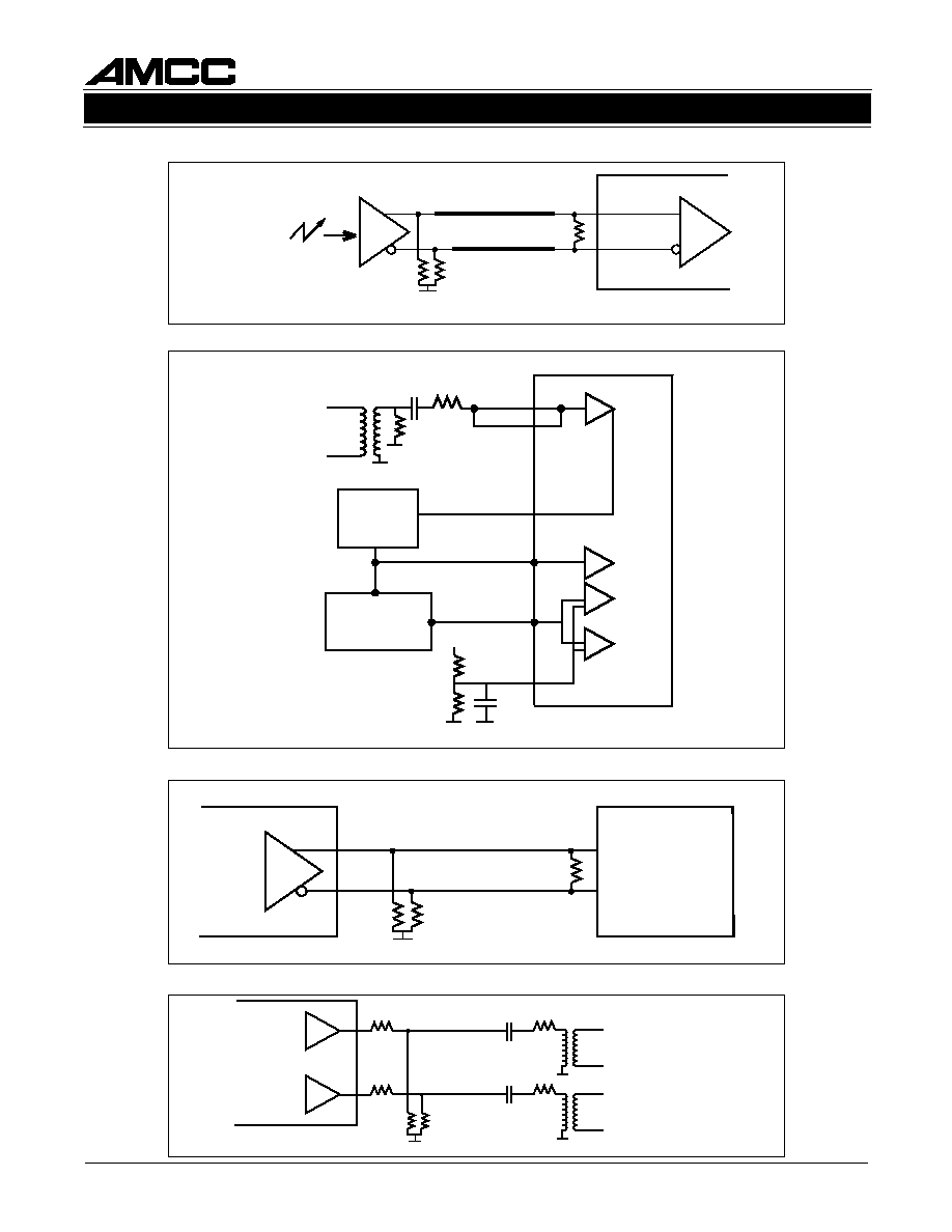
20
S3015/S3016
E4/STM-1/OC-3 ATM INTERFACE CIRCUITS
Figure 16. Differential ECL Input and Output Applications
XFRMDRVA
Cable Output
Monitor Output
XFRMDRVB
220
.01uf
.01uf
30
30
220
24
24
GND
GND
GND
Figure 19. S3015 Transformer Output Application
Electrical
to
Optical
330
330
GND
100
SERDATOP/N
Figure 18. S3015 Differential ECL Output Application
Figure 17. S3016 Transformer Input Application
S3016
BUFINA
BUFINB
Cable Input
LOSIN
LOSREF
+5V
.01
µ
F
LOSIN
COMPENSATOR
EQUALIZER
GND
GND
75
470
27pF
TRANSFORMER
BUFOUT
ANDATIN
GND
GND
ECL driver to
SERDATIP/N input
330
330
GND
100
SERDATIP
SERDATIN
Fiber Optic
Receiver

E4/STM-1/OC-3 ATM INTERFACE CIRCUITS
S3015/S3016
21
2
E/O
S3016
O/E
2
2
REFCKIN
SERCLKOP/N
S3026
SUNI
IGT
SYN155
REFCKIN
19.44 MHz
SERCLKOP/N
SERDATOP/N
SERDATIP/N
TX_CLK_+/≠
TX_DATA_+/≠
RX_CLK_+/≠
RX_DATA_+/≠
LOS
2
155 MHZ
2
2
155 MHZ
Figure 20. OC3 Application
Figure 21. STM-1 CMI, E4 Application
S3016
Equalizer
2
REFCKIN
SERCLKOP/N
S3015
SUNI-LITE
SUNI-PLUS
SABRE
S3011/12
REFCKIN
19.44 MHz
SERDATIP/N
SERDATOP/N
EQUALSEL
LOSREF
XFRMDRVB
SERDAT0P/N
SERDATIP/N
BUFIN
BUFOUT
ANDATIN
XFRMDRVA
TX_DATA_+/≠
REFCKIN
RX_CLK_+/≠
RX_DATA_+/≠
.01
µ
F
+5V
LOSIN
2
2
2
Cable
Output
Monitor
Output
Cable
Input
LOSIN
Compensator
GND
GND
GND
GND

22
S3015/S3016
E4/STM-1/OC-3 ATM INTERFACE CIRCUITS
GRADE
TRANSMITTER
3015
S ≠ Industrial/
commercial
A ≠ 52 TQFP TEP
w/DW0045-29 heatsink unattached
Ordering Information
GRADE
3016
RECEIVER
S ≠ Industrial/
commercial
X XXXX X / XX
Grade Part number Package H0 for no heatsink (identifier not marked on part)
A ≠ 52 TQFP TEP
w/DW0045-29 heatsink unattached
H0 ≠ No Heatsink
H0 ≠ No Heatsink
Processor Interface
PMC PM5345
SUNI
Saturn User Network Interface
PMC PM5346
SUNI-Lite
Saturn User Network Interface
PMC PM5347
SUNI-Plus
Saturn User Network Interface
IGT WAC-013-A
SONET LAN ATM Processor
TRANSWITCH SYN155
155 Mbit/s Synchronizer
TI SABRE TDC 1500
155 Mbit/s Processor
AMCC S3011/12
SONET/SDH/ATM 0C3 Transmitter & Receiver
Electrical Interface
Mini-Circuits
MCL TXI-R5
Wideband RF Transformer (Surface Mount)
Mini-Circuits
MCL TO-75
Wideband RF Transformer (Through-Hole)
Optical Interface
HP HFBR-520x
155 Mbit/s
Fiber Optic Transceiver
CTS ODL-1408X
155 Mbit/s
Fiber Optic Transceiver
Sumitomo SDM4123-XC
155 Mbit/s
Fiber Optic Transceiver
AMP 269039-1
155 Mbit/s
Fiber Optic Transceiver
Table 8. Suggested Interface Devices

E4/STM-1/OC-3 ATM INTERFACE CIRCUITS
S3015/S3016
23
AMCC is a registered trademark of Applied Micro Circuits Corporation.
Copyright Æ 1997 Applied Micro Circuits Corporation
June 2, 1997
AMCC reserves the right to make changes to its products or to discontinue any semiconductor product or service without notice, and
advises its customers to obtain the latest version of relevant information to verify, before placing orders, that the information being relied
on is current.
AMCC does not assume any liability arising out of the application or use of any product or circuit described herein, neither does it
convey any license under its patent rights nor the rights of others.
AMCC reserves the right to ship devices of higher grade in place of those of lower grade.
AMCC SEMICONDUCTOR PRODUCTS ARE NOT DESIGNED, INTENDED, AUTHORIZED, OR WARRANTED TO BE SUITABLE FOR
USE IN LIFE-SUPPORT APPLICATIONS, DEVICES OR SYSTEMS OR OTHER CRITICAL APPLICATIONS.
Applied Micro Circuits Corporation ∑ 6290 Sequence Dr., San Diego, CA 92121
Phone: (619) 450-9333 ∑ (800)755-2622 ∑ Fax: (619) 450-9885
http://www.amcc.com
C
E
R T I F I E
D
IS
O 9001