 | –≠–ª–µ–∫—Ç—Ä–æ–Ω–Ω—ã–π –∫–æ–º–ø–æ–Ω–µ–Ω—Ç: S3027 | –°–∫–∞—á–∞—Ç—å:  PDF PDF  ZIP ZIP |

1
S3028
SONET/SDH/ATM OC-3/OC-12 TRANSCEIVER
December 13, 1999 / Revision H
BiCMOS PECL CLOCK GENERATOR
Æ
DEVICE
SPECIFICATION
SONET/SDH/ATM OC-12 TRANSMITTER AND RECEIVER
S3028
FEATURES
∑ Complies with Bellcore and ITU-T
specifications
∑ Jitter generation better than ITU-T requirements
∑ On-chip high-frequency PLL for clock
generation
∑ Supports 155.52 Mbps (OC-3) and
622.08 Mbps (OC-12)
∑ Selectable reference frequencies of 19.44,
38.88, 51.84, or 77.76 MHz
∑ Interface to both PECL and TTL logic
∑ 4-bit or 8-bit OC-3 TTL datapath
∑ 8-bit OC-12 TTL datapath
∑ Compact 64 PQFP package
∑ Diagnostic loopback mode
∑ Line loopback mode
∑ Lock detect
∑ LOS input
∑ Low jitter PECL interface
∑ 0.9W typical power dissipation
∑ Loop Timing (S3028B only)
∑ Forward Clocking (S3028B only)
∑ "Squelched Clock" operation (S3028B only)
∑ 5 V Power supply
APPLICATIONS
∑ SONET/SDH-based transmission systems
∑ SONET/SDH modules
∑ SONET/SDH test equipment
∑ ATM over SONET/SDH
∑ Section repeaters
∑ Add Drop Multiplexers (ADM)
∑ Broad-band cross-connects
∑ Fiber optic terminators
∑ Fiber optic test equipment
Figure 1. System Block Diagram
SONET/SDH/ATM OC-3/OC-12 TRANSCEIVER
S3028
GENERAL DESCRIPTION
The S3028 SONET/SDH transceiver chip is a fully
integrated serialization/deserialization SONET
OC-12 (622.08 Mbit/s) and OC-3 (155.52 Mbit/s) in-
terface device. The chip performs all necessary
serial-to-parallel and parallel-to-serial functions in
conformance with SONET/SDH transmission stan-
dards. The device is suitable for SONET-based ATM
applications and can be used in conjunction with
AMCC's S3026 Clock Recovery Unit (CRU). Figure
1 shows a typical network application.
On-chip clock synthesis is performed by the high-
frequency phase-locked loop on the S3028
transceiver chip allowing the use of a slower external
transmit clock reference. The S3028 also performs
SONET/SDH frame detection. The chip can be used
with a 19.44, 38.88, 51.84 or 77.76 MHz reference
clock, in support of existing system clocking
schemes.
The low jitter PECL interface guarantees compliance
with the bit-error rate requirements of the Bellcore
and ITU-T standards. The S3028 is packaged in a
64 PQFP, offering designers a small package out-
line.
Since the S3028 jitter generation is better than the
ITU-T requirements over all reference frequencies,
the designer can meet the overall system require-
ment including the optical interface devices (refer to
Table 9 for jitter generation specifications).
Transceiver
S3028
Controller
Controller
Transceiver
S3028
8
8
8
8
Fiber
Optic
Module
Fiber
Optic
Module
S3026
S3026
Now available with
Loop Timing!
2
S3028
SONET/SDH/ATM OC-3/OC-12 TRANSCEIVER
December 13, 1999 / Revision H
SONET OVERVIEW
Synchronous Optical Network (SONET) is a stan-
dard for connecting one fiber system to another at
the optical level. SONET, together with the Synchro-
nous Digital Hierarchy (SDH) administered by the
ITU-T, forms a single international standard for fiber
interconnect between telephone networks of differ-
ent countries. SONET is capable of accommodating
a variety of transmission rates and applications.
The SONET standard is a layered protocol with four
separate layers defined. These are:
∑ Photonic
∑ Section
∑ Line
∑ Path
Figure 2 shows the layers and their functions. Each of
the layers has overhead bandwidth dedicated to admin-
istration and maintenance. The photonic layer simply
handles the conversion from electrical to optical and
back with no overhead. It is responsible for transmitting
the electrical signals in optical form over the physical
media. The section layer handles the transport of the
framed electrical signals across the optical cable
from one end to the next. Key functions of this layer
are framing, scrambling, and error monitoring. The
line layer is responsible for the reliable transmission
of the path layer information stream carrying voice,
data, and video signals. Its main functions are syn-
chronization, multiplexing, and reliable transport.
The path layer is responsible for the actual transport
of services at the appropriate signaling rates.
Data Rates and Signal Hierarchy
Table 1 contains the data rates and signal designations
of the SONET hierarchy. The lowest level is the basic
SONET signal referred to as the synchronous trans-
port signal level-1 (STS-1). An STS-
N signal is made
up of
N byte-interleaved STS-1 signals. The optical
counterpart of each STS-
N signal is an optical car-
rier level-
N signal (OC-N). The S3028 chip supports
OC-3 and OC-12 rates (155.52 and 622.08 Mbit/s).
Frame and Byte Boundary Detection
The SONET/SDH fundamental frame format for STS-
12 consists of 36 transport overhead bytes followed
by Synchronous Payload Envelope (SPE) bytes.
This pattern of 36 overhead and 1044 SPE bytes is
repeated nine times in each frame. Frame and byte
boundaries are detected using the A1 and A2 bytes
found in the transport overhead. (See Figure 3.)
For more details on SONET operations, refer to the
Bellcore SONET standard document.
Elec.
CCITT
Optical Data Rate (Mbit/s)
STS-1
OC-1
51.84
STS-3
STM-1
OC-3
155.52
STS-12
STM-4
OC-12
622.08
STS-24
STM-8
OC-24
1244.16
STS-48 STM-16
OC-48 2488.32
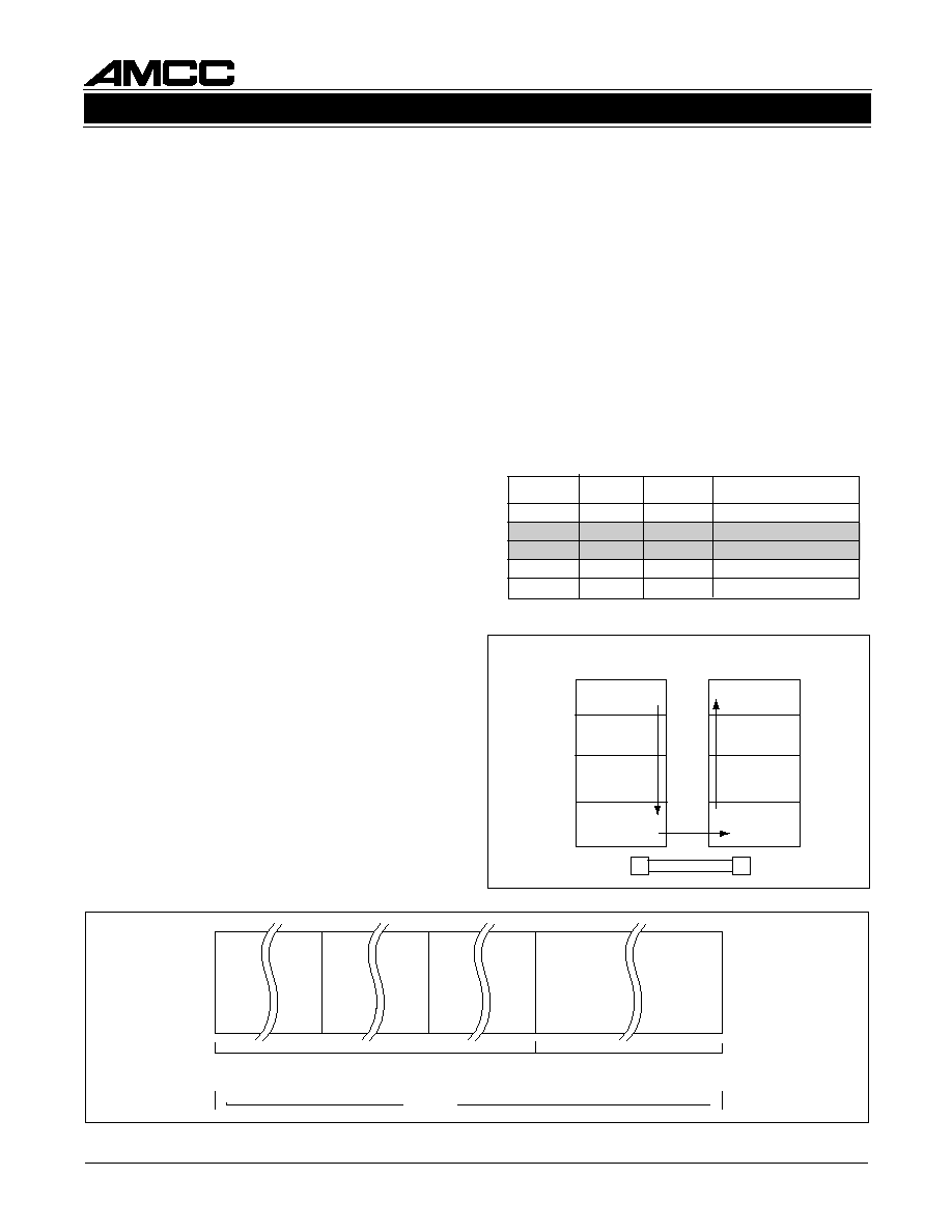
Table 1. SONET Signal Hierarchy
Figure 2. SONET Structure
Figure 3. STS≠12/OC≠12 Frame Format
9 Rows
12 A1
Bytes
12 A2
Bytes
A1 A1
A1 A1
A2 A2
A2 A2
Transport Overhead 36 Columns
36 x 9 = 324 bytes
Synchronous Payload Envelope 1044 Columns
1044 x 9 = 9396 bytes
125
µ
sec
v
v
0 bps
End Equipment
Payload to
SPE mapping
Maintenance,
protection,
switching
Optical
transmission
Scrambling,
framing
Fiber Cable
End Equipment
Section layer
Photonic layer
Line layer
Path layer
Path layer
Section layer
Photonic layer
Line layer
Layer Overhead
(Embedded Ops
Channel)
Functions
576 Kbps
192 Kbps
3
S3028
SONET/SDH/ATM OC-3/OC-12 TRANSCEIVER
December 13, 1999 / Revision H
S3028 OVERVIEW
The S3028 transceiver implements SONET/SDH se-
rialization/deserialization, transmission, and frame
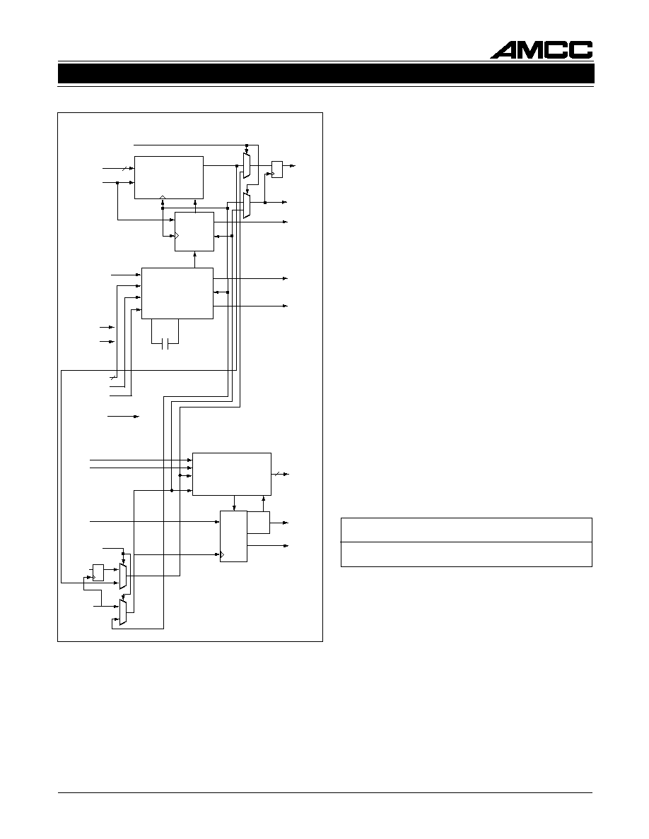
detection/recovery functions. The block diagram in
Figure 4 shows basic operation of the chip. This chip
can be used to implement the front end of SONET
equipment, which consists primarily of the serial
transmit interface and the serial receive interface.
The chip handles all the functions of these two
elements, including parallel-to-serial and serial-to-
parallel conversion, clock generation, and system
timing. The system timing circuitry consists of man-
agement of the data stream, framing, and clock
distribution throughout the front end.
The S3028 is divided into a transmitter section and a
receiver section. The sequence of operations is as follows:
Transmitter Operations:
1. 4 or 8-bit parallel input
2. Parallel-to-serial conversion
3. Serial output
Receiver Operations:
1. Serial input
2. Frame detection
3. Serial-to-parallel conversion
4. 4 or 8-bit parallel output
Internal clocking and control functions are transpar-
ent to the user. Details of data timing can be seen in
Figures 7 through 10.
Figure 4. S3028 Transceiver Functional Block Diagram
AMCC S3026 622/155 Mbit/s
Clock Recovery Device
AMCC S3027 622/155 Mbit/s
Clock Recovery Device
AMCC
CONGO (S1201)
POS/ATM SONET Mapper
AMCC
NILE (S1202)
ATM SONET Mapper
Suggested Interface Devices
1:8 SERIAL
TO PARALLEL
TIMING
GEN
M
U
X
RSDP/N
FRAME
BYTE
DETECT
DLEB
OOF
FP
POUT[7:0]
8
RSCLKP/N
SDTTL
SDPECL
M
U
X
M
U
X
M
U
X
POCLK
8
PIN[7:0]
LLEB
8:1 PARALLEL
TO SERIAL
TSDP/N
PICLK
BUSWIDTH
TIMING
GEN
PCLK
LOCKDET
19MCK
CLOCK
SYNTHESIZER
RSTB
D
D
2
TSCLKP/N
TESTEN
TESTRST
REFSEL[1:0]
MODE
REFCLKP/N
CAP1
CAP2
Transmitter
Receiver
4
S3028
SONET/SDH/ATM OC-3/OC-12 TRANSCEIVER
December 13, 1999 / Revision H
TRANSCEIVER FUNCTIONAL
DESCRIPTION
TRANSMITTER OPERATION
The S3028 transceiver chip performs the serializing
stage in the processing of a transmit SONET STS-3 or
STS-12 bit serial data stream. It converts the 8-bit par-
allel 19.44, 38.88 or 77.76 Mbyte/sec data stream
into bit serial format at 155.52 or 622.08 Mbit/sec.
Diagnostic loopback is provided (transmitter to re-
ceiver). Line loopback is also provided (receiver-to-
transmitter).
A high-frequency bit clock can be generated from a
19.44, 38.88, 51.84 or 77.76 MHz frequency reference
by using an integral frequency synthesizer consisting of
a phase-locked loop circuit with a divider in the loop.
Clock Synthesizer
The clock synthesizer, shown in the block diagram in
Figure 4, is a monolithic PLL that generates the
serial output clock phase synchronized with the input
Reference Clock (REFCLK). There are three select-
able output clock frequencies that are synthesizable
from any of four selectable reference frequencies for
SONET/SDH operation.
The MODE inputs select the output serial clock fre-
quency to be 622.08 MHz for STS-12, or 155.52
MHz for STS-3. Their frequencies are selected as
shown in Table 2.
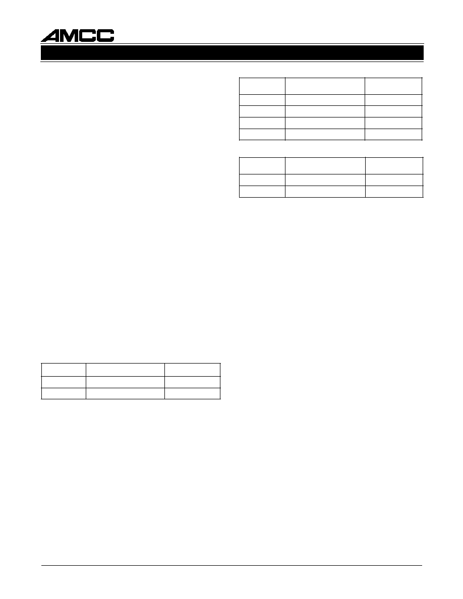
Table 2. Clock Frequency Options
In order to meet the 0.01 UI SONET jitter generation
specifications, the maximum reference clock jitter
must be guaranteed over the 12 kHz to 1 MHz band-
width for the STS-3 operating mode. For details of
reference clock jitter requirements, see Table 4.
The on≠chip PLL consists of a phase detector, which
compares the phase relationship between the VCO out-
put and the REFCLK input, a loop filter which converts
the phase detector output into a smooth DC voltage, and
a VCO, whose frequency is varied by this voltage.
The loop filter generates a VCO control voltage based
on the average DC level of the phase discriminator
output pulses. The loop filter's corner frequency is
optimized to minimize output phase jitter.
Timing Generator
The timing generator function, seen in Figure 4, pro-
vides two separate functions. It provides a byte rate
version of the TSCLK, and a mechanism for aligning
the phase between the incoming byte clock and the
clock which loads the parallel-to-serial shift register.
The PCLK output is a byte rate version of TSCLK.
For STS-12, the PCLK frequency is 77.76 MHz, and
for STS-3, its frequency is 19.44 or 38.88 MHz.
PCLK is intended for use as an 8-bit parallel clock for
upstream multiplexing and overhead processing cir-
cuits. Using PCLK for upstream circuits will ensure a
stable frequency and phase relationship between the
data coming into and leaving the S3028 device.
In the parallel-to-serial conversion process, the in-
coming data is passed from the PICLK 8-bit parallel
clock timing domain to the internally generated serial
clock timing domain, which is phase aligned to
TSCLK.
Table 3. Reference Frequency Options
Table 4. Reference Jitter Limits
The REFSEL[1:0] inputs in combination with the MODE
input select the ratio between the output clock fre-
quency and the reference input frequency, as shown
in Table 3. This ratio is adjusted for each of the four
operating modes so that the reference frequency se-
lected by the REFSEL[1:0] is the same for all
modes.
The REFCLK input must be generated from a differ-
ential PECL crystal oscillator which has a frequency
accuracy that meets the value specified in Table 9 in
order for the TSCLK frequency to have the same
accuracy required for operation in a SONET system.
E
D
O
M
y
c
n
e
u
q
e
r
F
k
c
o
l
C
t
u
p
t
u
O
e
d
o
M
g
n
i
t
a
r
e
p
O
1
z
H
M
8
0
.
2
2
6
2
1
-
S
T
S
0
z
H
M
2
5
.
5
5
1
3
-
S
T
S
y
c
n
e
u
q
e
r
F
d
n
a
B
e
c
n
e
r
e
f
e
R
m
u
m
i
x
a
M
r
e
t
t
i
J
k
c
o
l
C
e
d
o
M
g
n
i
t
a
r
e
p
O
z
H
M
5
o
t
z
H
k
2
1
s
m
r
s
p
4
1
2
1
-
S
T
S
z
H
M
1
o
t
z
H
k
2
1
s
m
r
s
p
6
5
3
-
S
T
S
]
0
:
1
[
L
E
S
F
E
R
k
c
o
l
C
e
c
n
e
r
e
f
e
R
y
c
n
e
u
q
e
r
F
e
d
o
M
g
n
i
t
a
r
e
p
O
0
0
z
H
M
4
4
.
9
1
3
-
S
T
S
,
2
1
-
S
T
S
1
0
z
H
M
8
8
.
8
3
3
-
S
T
S
,
2
1
-
S
T
S
0
1
z
H
M
4
8
.
1
5
3
-
S
T
S
,
2
1
-
S
T
S
1
1
z
H
M
6
7
.
7
7
2
1
-
S
T
S

5
S3028
SONET/SDH/ATM OC-3/OC-12 TRANSCEIVER
December 13, 1999 / Revision H
RECEIVER OPERATION
The S3028 transceiver chip provides the first stage
of the digital processing of a receive SONET STS-3
or STS-12 bit-serial stream. It converts the bit-serial
155.52 or 622.08 Mbit/sec data stream into a 19.44,
38.88 or 77.76 Mbyte/sec parallel data format. A
loopback mode is provided for diagnostic loopback
(transmitter to receiver). An additional loopback mode
is provided for line loopback (receiver to transmitter).
Frame and Byte Boundary Detection
The frame and byte boundary detection circuitry
searches the incoming data for three consecutive A1
bytes followed immediately by three consecutive A2
bytes. Framing pattern detection is enabled and dis-
abled by the Out Of Frame (OOF) input. Detection is
enabled by a rising edge on OOF, and remains en-
abled for the duration that OOF is set High. It is
disabled when a framing pattern is detected after
OOF is set Low. When framing pattern detection is
enabled, the framing pattern is used to locate byte
and frame boundaries in the incoming data stream
(RSD or looped transmitter data). The timing genera-
tor block takes the located byte boundary and uses it
to block the incoming data stream into bytes for out-
put on the parallel output data bus (POUT[7:0]).
When framing pattern detection is enabled, the
frame boundary is reported on the Frame Pulse (FP)
output when any 48-bit pattern matching the framing
pattern is detected on the incoming data stream.
When framing pattern detection is disabled, the byte
boundary is frozen to the location found when detec-
tion was previously enabled. Only framing patterns
aligned to the fixed byte boundary are indicated on
the FP output.
The probability that random data in an STS-3 or
STS-12 stream will generate the 48-bit framing pat-
tern is extremely small. It is highly improbable that a
mimic pattern would occur within one frame of data.
Therefore, the time to match the first frame pattern
and to verify it with down-stream circuitry, at the next
occurrence of the pattern, is expected to be less
than the required 250
µ
s, even for extremely high bit
error rates.
Once down-stream overhead circuitry has verified
that frame and byte synchronization are correct, the
OOF input can be set low to disable the frame
search process from trying to synchronize to a mimic
frame pattern.
Serial to Parallel Converter
The serial to parallel converter consists of three 8-bit
registers. The first is a serial-in, parallel-out shift reg-
ister, which performs serial to parallel conversion
clocked by the clock recovery block. The second is
an 8-bit internal holding register, which transfers
data from the serial to parallel register on byte
boundaries as determined by the frame and byte
boundary detection block. On the falling edge of the
free running POCLK, the data in the holding register
is transferred to an output holding register which
drives POUT[7:0].
The delay through the serial to parallel converter can
vary from 1.5 to 2.5 byte periods (12 to 20 serial bit
periods) measured from the first bit of an incoming
byte to the beginning of the parallel output of that
byte. The variation in the delay is dependent on the
alignment of the internal parallel load timing, which is
synchronized to the data byte boundaries, with re-
spect to the falling edge of POCLK, which is
independent of the byte boundaries. The advantage of
this serial to parallel converter is that POCLK is neither
truncated nor extended during reframe sequences.
The timing generator also produces a feedback ref-
erence clock to the clock synthesizer. A counter
divides the synthesized clock down to the same fre-
quency as the Reference Clock REFCLK. The PLL
in the clock synthesizer maintains the stability of the
synthesized clock by comparing the phase of the
internal clock with that of the reference clock
(REFCLK). The modulus of the counter is a function
of the reference clock frequency and the operating
frequency.
Parallel-to-Serial Converter
The parallel-to-serial converter shown in Figure 4 is
comprised of two 8-bit wide registers. The first regis-
ter latches the data from the PIN[7:0] bus on the
rising edge of PICLK. The second register is a paral-
lel loadable shift register which takes its parallel
input from the first register.
An internally generated byte clock, which is phase
aligned to the transmit serial clock as described in
the Timing Generator description, activates the paral-
lel data transfer between registers. The serial data is
shifted out of the second register at the TSCLK rate.