 | –≠–ª–µ–∫—Ç—Ä–æ–Ω–Ω—ã–π –∫–æ–º–ø–æ–Ω–µ–Ω—Ç: S3028 | –°–∫–∞—á–∞—Ç—å:  PDF PDF  ZIP ZIP |
1
S3029
SONET/SDH/ATM 155 MBIT/S QUAD TRANSCEIVER
February 19, 1999 / Revision B
BiCMOS PECL CLOCK GENERATOR
DEVICE
SPECIFICATION
SONET/SDH/ATM 155 MBIT/S QUAD TRANSCEIVER
S3029
Æ
FEATURES
∑
Complies with ANSI, Bellcore, and ITU-T
specifications for jitter tolerance, jitter generation
∑
Five on-chip high frequency PLLs with
internal loop filters for clock recovery
∑
Supports clock recovery for STS-3/STM-1
(155.52 Mbit/s) NRZ data
∑
Clock Multiplier PLL for transmit clock
generation
∑
19.44 or 51.84 MHz reference frequency
∑
Lock detect--monitors run length and
frequency
∑
Low-jitter differential interface
∑
3.3V supply
∑
Available in a 64-pin TQFP package
∑
Compatible with IgT WAC-413 ATM Quad-
UNI processor
GENERAL DESCRIPTION
The function of the S3029 clock synthesis and recov-
ery unit is to derive high speed timing signals for
SONET/SDH-based equipment. The S3029 is imple-
mented using AMCC's proven Phase Locked Loop
(PLL) technology.
The S3029 receives four STS-3/STM-1 scrambled NRZ
signals and recovers the clock from the data and
generates a 155 MHz transmit clock. The chip out-
puts a differential PECL bit clock and retimed data.
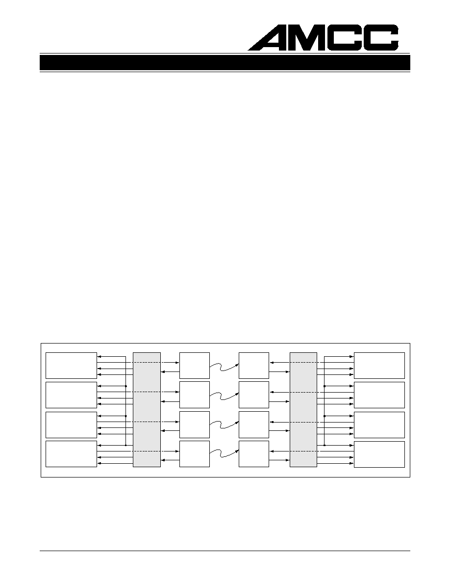
Figure 1 shows a typical network application.
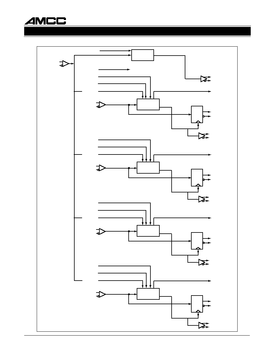
The S3029 utilizes five on-chip PLLs which consist of
a phase detector, a loop filter, and a voltage con-
trolled oscillator (VCO). The phase detector
compares the phase relationship between the VCO
output and the serial data input. A loop filter converts
the phase detector output into a smooth DC voltage,
and the DC voltage is input to the VCO whose fre-
quency is varied by this voltage. A block diagram is
shown in Figure 2. There is a single clock multiplier
PLL which generates a 155 MHz transmit clock from
a 19.44 or 51.84 MHz input.
Figure 1. System Block Diagram
155 Mbp/s
Network
Interface Processor
155 Mbp/s
Network
Interface Processor
155 Mbp/s
Network
Interface Processor
155 Mbp/s
Network
Interface Processor
TXCLK
TXDATA
RXDATA
RXCLK
Optical
Transceiver
Optical
Transceiver
S3029
S3029
Optical
Transceiver
Optical
Transceiver
RX
RX
RX
RX
TXCLK
TXDATA
RXDATA
RXCLK
TXCLK
TXDATA
RXDATA
RXCLK
TXCLK
TXDATA
RXDATA
RXCLK
155 Mbp/s
Network
Interface Processor
155 Mbp/s
Network
Interface Processor
155 Mbp/s
Network
Interface Processor
155 Mbp/s
Network
Interface Processor
TXCLK
TXDATA
RXDATA
RXCLK
Optical
Transceiver
Optical
Transceiver
Optical
Transceiver
Optical
Transceiver
RX
RX
RX
RX
TXCLK
TXDATA
RXDATA
RXCLK
TXCLK
TXDATA
RXDATA
RXCLK
TXCLK
TXDATA
RXDATA
RXCLK
2
S3029
SONET/SDH/ATM 155 MBIT/S QUAD TRANSCEIVER
February 19, 1999 / Revision B
Figure 2. Functional Block Diagram
PLL CLOCK
RECOVERY
PLL CLOCK
MULTIPLIER
D
BITCLK
Q
QN
SERDATIP0
REFCLK
LCKREFN0
155 MHz CLK
SERDATIN0
REFCKINP
REFCKINN
SERDATIP1
SERDATIN1
SERDATIP2
SERDATIN2
SERDATIP3
SERDATIN3
LOCKDET0
SERCLKOP0
SERCLKON0
TXCLKOP
TXCLKON
PLL CLOCK
RECOVERY
D
BITCLK
Q
QN
REFCLK
LCKREFN1
LOCKDET1
SERCLKOP1
SERCLKON1
PLL CLOCK
RECOVERY
D
BITCLK
Q
QN
REFCLK
LCKREFN2
LOCKDET2
SERCLKOP2
SERCLKON2
PLL CLOCK
RECOVERY
D
BITCLK
Q
QN
REFCLK
LCKREFN3
SD3
SD2
SD1
SD0
TSTCLKEN
REFSEL
LOCKDET3
SERDATOP3
SERCLKOP3
SERCLKON3
SERDATON3
SERDATOP1
SERDATON1
SERDATOP0
SERDATON0
SERDATOP2
SERDATON2
3
S3029
SONET/SDH/ATM 155 MBIT/S QUAD TRANSCEIVER
February 19, 1999 / Revision B
S3029 OVERVIEW
The S3029 supports clock recovery for the STS-3/
STM-1 data rate. The LVPECL differential serial data
is input to the chip and clock recovery is performed on
the incoming data stream. An external reference clock
is required to minimize the PLL lock time and provide
a stable output clock source in the absence of serial
input data. Retimed data and clock are output from the
S3029.
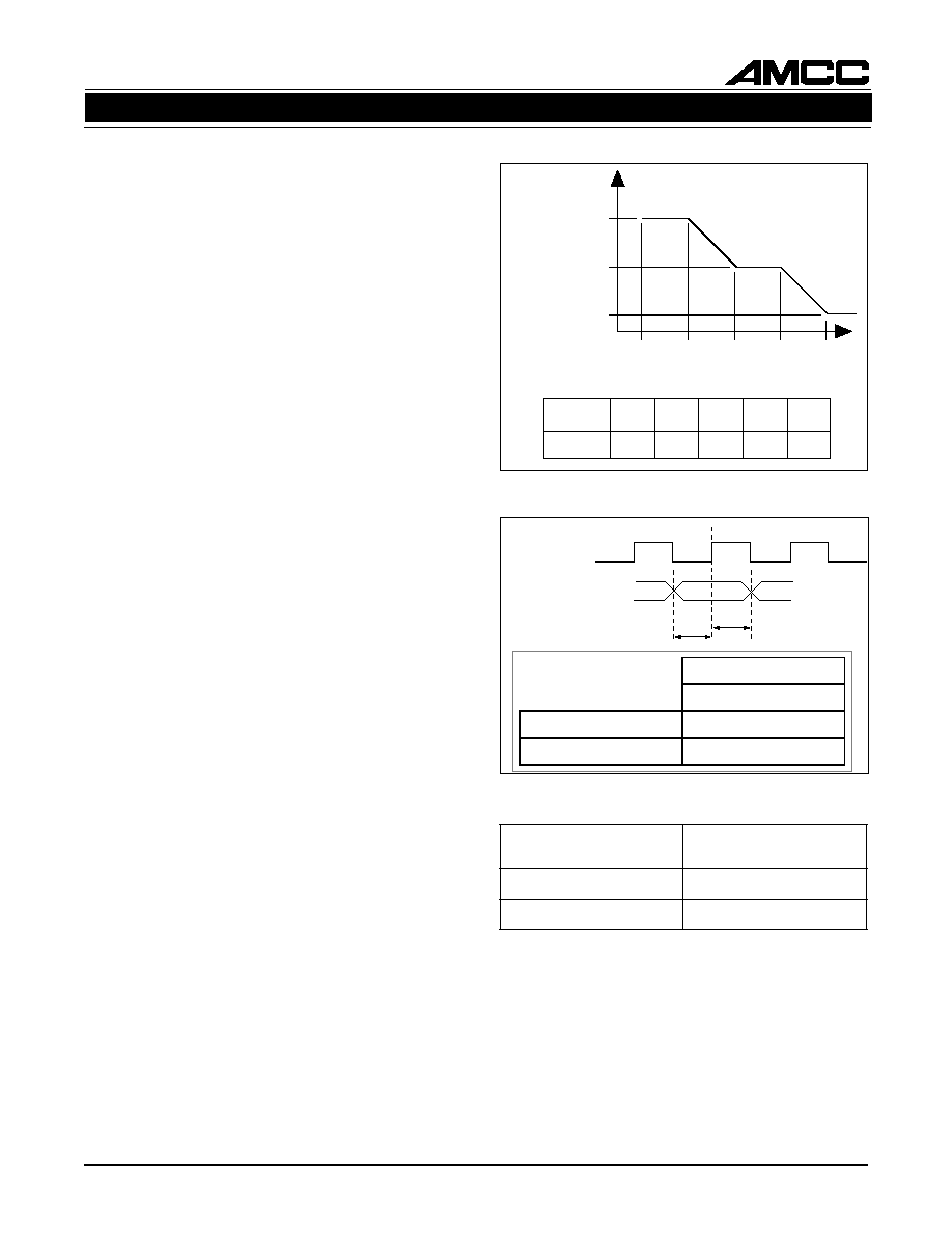
CHARACTERISTICS
Performance
The S3029 PLL complies with the minimum jitter tol-
erance for clock recovery proposed for SONET/SDH
equipment defined by the T1X1.6/91-022 document,
when used with differential inputs and outputs as
shown in Figure 3.
Input Jitter Tolerance
Input jitter tolerance is defined as the peak to peak
amplitude of sinusoidal jitter applied on the input sig-
nal that causes an equivalent 1 dB optical/electrical
power penalty. SONET input jitter tolerance require-
ments are shown in Figure 3. The measurement
condition is the input jitter amplitude which causes an
equivalent of 1 dB power penalty.
Serial Data Output Set-up and Hold Time
The output set-up and hold times are represented by
the waveforms shown in Figure 4.
Figure 4. Clock Output to Data Transition Delay
Output Frequency
155.52 MHz
SERDATOP/N Setup Time
2.5 ns
SERDATOP/N Hold Time
2.5 ns
t su
t h
SERCLKOP/N
SERDATOP/N
Figure 3. Input Jitter Tolerance Specification
f0
f1
f2
f3
ft
0.15
1.5
15
Sinusodal
Input Jitter
Amplitude
(UI p-p)
Frequency
OC/STS
Level
f0
(Hz)
f2
(Hz)
f3
(kHz)
ft
(kHz)
f1
(Hz)
3
10
30
300
6.5
75
L
E
S
F
E
R
k
c
o
l
C
e
c
n
e
r
e
f
e
R
)
z
H
M
(
y
c
n
e
u
q
e
r
F
0
z
H
M
4
4
.
9
1
1
z
H
M
4
8
.
1
5
Table 1.

4
S3029
SONET/SDH/ATM 155 MBIT/S QUAD TRANSCEIVER
February 19, 1999 / Revision B
e
m
a
N
n
i
P
l
e
v
e
L
O
/
I
#
n
i
P
n
o
i
t
p
i
r
c
s
e
D
N
/
P
N
I
K
C
F
E
R
.
f
f
i
D
L
C
E
P
V
L
I
4
5
,
3
5
e
t
a
r
e
n
e
g
o
t
d
e
s
u
t
u
p
n
i
z
H
M
4
8
.
1
5
r
o
4
4
.
9
1
.
k
c
o
l
C
e
c
n
e
r
e
f
e
R
e
h
t
s
a
d
e
s
u
o
s
l
a
s
i
t
u
p
n
i
s
i
h
T
.
k
c
o
l
c
t
i
m
s
n
a
r
t
z
H
M
5
5
1
e
h
t
a
t
a
d
l
a
i
r
e
s
f
o
e
c
n
e
s
b
a
e
h
t
n
i
k
c
o
l
c
t
i
b
l
a
n
r
e
t
n
i
e
h
t
r
o
f
e
c
n
e
r
e
f
e
r
.
e
d
o
m
y
r
e
v
o
c
e
r
k
c
o
l
c
n
i
t
e
s
e
r
g
n
i
r
u
d
r
o
0
N
/
P
I
T
A
D
R
E
S
1
N
/
P
I
T
A
D
R
E
S
2
N
/
P
I
T
A
D
R
E
S
3
N
/
P
I
T
A
D
R
E
S
.
f
f
i
D
L
C
E
P
V
L
I
2
,
1
8
,
7
6
1
,
5
1
1
2
,
2
2
e
s
e
h
t
n
o
s
n
o
i
t
i
s
n
a
r
t
e
h
t
m
o
r
f
d
e
r
e
v
o
c
e
r
s
i
k
c
o
l
C
.
n
I
a
t
a
D
l
a
i
r
e
S
.
s
t
u
p
n
i
N
E
K
L
C
T
S
T
L
T
T
V
L
I
3
o
t
t
s
e
t
n
o
i
t
c
u
d
o
r
p
g
n
i
r
u
d
d
e
s
U
.
h
g
i
H
e
v
i
t
c
A
.
e
l
b
a
n
E
k
c
o
l
C
t
s
e
T
.
n
o
i
t
a
r
e
p
o
l
a
m
r
o
n
r
o
f
d
n
u
o
r
g
o
t
e
i
T
.
L
L
P
e
h
t
n
i
O
C
V
e
h
t
s
s
a
p
y
b
0
D
S
1
D
S
2
D
S
3
D
S
L
C
E
P
V
L
I
6
5
5
5
2
5
1
5
e
b
o
t
t
u
p
n
i
L
C
E
K
0
1
d
e
d
n
e
-
e
l
g
n
i
s
A
.
h
g
i
H
e
v
i
t
c
A
.
t
c
e
t
e
D
l
a
n
g
i
S
e
t
a
c
i
d
n
i
o
t
e
l
u
d
o
m
r
e
v
i
e
c
e
r
l
a
c
i
t
p
o
l
a
n
r
e
t
x
e
e
h
t
y
b
n
e
v
i
r
d
e
h
t
,
e
v
i
t
c
a
n
i
s
i
D
S
n
e
h
W
.
r
e
w
o
p
l
a
c
i
t
p
o
d
e
v
i
e
c
e
r
f
o
n
o
i
t
c
e
t
e
d
y
ll
a
n
r
e
t
n
i
e
b
ll
i
w
s
n
i
p
)
N
/
P
I
T
A
D
R
E
S
(
n
I
a
t
a
D
l
a
i
r
e
S
e
h
t
n
o
a
t
a
d
L
L
P
e
h
t
d
n
a
,
w
o
l
d
e
c
r
o
f
T
E
D
K
C
O
L
,
o
r
e
z
t
n
a
t
s
n
o
c
a
o
t
d
e
c
r
o
f
n
o
a
t
a
d
,
e
v
i
t
c
a
s
i
D
S
n
e
h
W
.
t
u
p
n
i
K
C
F
E
R
e
h
t
o
t
k
c
o
l
o
t
d
e
c
r
o
f
s
a
h
n
i
p
s
i
h
T
.
y
ll
a
m
r
o
n
d
e
s
s
e
c
o
r
p
e
b
ll
i
w
s
n
i
p
N
/
P
I
T
A
D
R
E
S
e
h
t
K
1
l
a
n
r
e
t
n
i
n
a
.
n
w
o
d
-
ll
u
p
0
N
F
E
R
K
C
L
1
N
F
E
R
K
C
L
2
N
F
E
R
K
C
L
3
N
F
E
R
K
C
L
L
T
T
V
L
I
4
6
3
6
0
6
9
5
e
c
r
o
f
ll
i
w
t
u
p
n
i
s
i
h
t
,
e
v
i
t
c
a
n
e
h
W
.
w
o
L
e
v
i
t
c
A
.
e
c
n
e
r
e
f
e
R
o
t
k
c
o
L
n
a
s
a
h
t
u
p
n
i
s
i
h
T
.
k
c
o
l
c
e
c
n
e
r
e
f
e
r
l
a
c
o
l
e
h
t
o
t
k
c
o
l
o
t
U
R
C
e
h
t
.
d
e
s
u
t
o
n
f
i
d
e
t
c
e
n
n
o
c
n
u
t
f
e
l
e
b
y
a
m
d
n
a
p
u
-
ll
u
p
K
1
l
a
n
r
e
t
n
i
L
E
S
F
E
R
L
T
T
V
L
I
6
e
h
t
f
o
y
c
n
e
u
q
e
r
f
e
h
t
s
t
c
e
l
e
s
t
u
p
n
i
s
i
h
T
.
t
c
e
l
e
S
e
c
n
e
r
e
f
e
R
.
)
1
e
l
b
a
T
e
e
S
(
.
P
/
N
I
K
C
F
E
R
0
T
E
D
K
C
O
L
1
T
E
D
K
C
O
L
2
T
E
D
K
C
O
L
3
T
E
D
K
C
O
L
L
T
T
V
L
O
9
4
1
7
1
0
2
h
g
i
h
t
e
S
.
r
o
t
a
c
i
d
n
i
y
r
e
v
o
c
e
r
k
c
o
l
C
.
h
g
i
H
e
v
i
t
c
A
.
t
c
e
t
e
D
k
c
o
L
g
n
i
m
o
c
n
i
e
h
t
o
t
n
o
d
e
k
c
o
l
s
a
h
y
r
e
v
o
c
e
r
k
c
o
l
c
l
a
n
r
e
t
n
i
e
h
t
n
e
h
w
t
u
p
t
u
o
s
i
h
T
.
t
u
p
t
u
o
s
u
o
n
o
r
h
c
n
y
s
a
n
a
s
i
T
E
D
K
C
O
L
.
m
a
e
r
t
s
a
t
a
d
n
i
;
w
o
l
s
i
D
S
n
e
h
w
r
o
,
w
o
l
s
i
N
F
E
R
K
C
L
n
e
h
w
d
e
t
r
e
s
s
a
e
d
s
i
a
t
a
d
e
h
t
n
e
h
W
.
k
c
o
l
c
e
c
n
e
r
e
f
e
r
e
h
t
o
t
s
k
c
o
l
L
L
P
e
h
t
e
s
a
c
h
c
i
h
w
f
o
e
g
n
a
r
e
r
u
t
p
a
c
e
h
t
n
i
h
t
i
w
t
o
n
s
i
t
u
p
n
i
N
/
P
I
T
A
D
R
E
S
e
h
t
f
o
e
t
a
r
s
i
a
t
a
d
r
e
p
o
r
p
li
t
n
u
e
l
g
g
o
t
ll
i
w
t
u
p
t
u
o
T
E
D
K
C
O
L
e
h
t
,
L
L
P
e
h
t
.
d
e
r
o
t
s
e
r
0
N
/
P
O
T
A
D
R
E
S
1
N
/
P
O
T
A
D
R
E
S
2
N
/
P
O
T
A
D
R
E
S
3
N
/
P
O
T
A
D
R
E
S
.
f
f
i
D
L
C
E
P
V
L
O
3
4
,
4
4
9
3
,
0
4
9
2
,
0
3
5
2
,
6
2
e
h
t
f
o
n
o
i
s
r
e
v
d
e
y
a
l
e
d
e
h
t
s
i
l
a
n
g
i
s
s
i
h
T
.
t
u
O
a
t
a
D
l
a
i
r
e
S
f
o
e
g
d
e
g
n
il
l
a
f
e
h
t
n
o
d
e
t
a
d
p
u
)
I
T
A
D
R
E
S
(
m
a
e
r
t
s
a
t
a
d
g
n
i
m
o
c
n
i
.
)
P
O
K
L
C
R
E
S
(
t
u
O
k
c
o
l
C
l
a
i
r
e
S
0
N
/
P
O
K
L
C
R
E
S
1
N
/
P
O
K
L
C
R
E
S
2
N
/
P
O
K
L
C
R
E
S
3
N
/
P
O
K
L
C
R
E
S
.
f
f
i
D
L
C
E
P
V
L
O
5
4
,
6
4
7
3
,
8
3
1
3
,
2
3
3
2
,
4
2
a
t
a
D
l
a
i
r
e
S
h
t
i
w
d
e
n
g
il
a
e
s
a
h
p
s
i
l
a
n
g
i
s
s
i
h
T
.
t
u
O
k
c
o
l
C
l
a
i
r
e
S
n
e
h
W
.
h
g
i
H
s
i
)
T
E
D
K
C
O
L
(
t
c
e
t
e
D
k
c
o
L
n
e
h
w
)
O
T
A
D
R
E
S
(
t
u
O
h
t
i
w
s
u
o
n
o
r
h
c
n
y
s
s
i
t
u
O
k
c
o
l
C
l
a
i
r
e
S
,
w
o
L
s
i
t
c
e
t
e
D
k
c
o
L
.
)
N
I
K
C
F
E
R
(
k
c
o
l
C
e
c
n
e
r
e
f
e
R
N
/
P
O
K
L
C
X
T
.
f
f
i
D
L
C
E
P
V
L
O
9
4
,
0
5
d
e
s
u
e
b
n
a
c
h
c
i
h
w
k
c
o
l
c
z
H
M
5
5
1
a
s
i
s
i
h
T
.
t
u
O
k
c
o
l
C
t
i
m
s
n
a
r
T
.
c
i
g
o
l
r
e
t
t
i
m
s
n
a
r
t
e
h
t
r
o
f
e
c
r
u
o
s
k
c
o
l
c
a
s
a
r
e
ll
o
r
t
n
o
c
e
h
t
y
b
S3029 Transceiver Pin Assignment and Descriptions

5
S3029
SONET/SDH/ATM 155 MBIT/S QUAD TRANSCEIVER
February 19, 1999 / Revision B
e
m
a
N
n
i
P
l
e
v
e
L
O
/
I
#
n
i
P
n
o
i
t
p
i
r
c
s
e
D
W
O
P
o
X
T
0
W
O
P
o
U
R
C
1
W
O
P
o
U
R
C
2
W
O
P
o
U
R
C
3
W
O
P
o
U
R
C
l
a
t
i
g
i
D
r
e
w
o
P
--
8
4
2
4
6
3
4
3
8
2
)
g
n
il
p
u
o
c
e
d
l
a
u
d
i
v
i
d
n
i
(
V
3
.
3
+
D
R
G
o
X
T
0
D
R
G
o
U
R
C
1
D
R
G
o
U
R
C
2
D
R
G
o
U
R
C
3
D
R
G
o
U
R
C
l
a
t
i
g
i
D
d
n
u
o
r
G
--
7
4
1
4
5
3
3
3
7
2
)
d
n
u
o
r
g
(
V
0
C
C
V
O
C
V
C
C
V
A
P
O
0
W
O
P
U
R
C
A
1
W
O
P
U
R
C
A
2
W
O
P
U
R
C
A
3
W
O
P
U
R
C
A
g
o
l
a
n
A
r
e
w
o
P
--
8
5
2
6
4
0
1
2
1
8
1
d
n
a
)
6
0
A
2
3
M
L
B
a
t
a
r
u
M
.
g
.
e
(
d
a
e
b
e
t
i
r
r
e
F
l
a
u
d
i
v
i
d
n
i
a
i
v
V
3
.
3
+
.
g
n
il
p
u
o
c
e
d
l
a
u
d
i
v
i
d
n
i
D
R
G
O
C
V
D
R
G
A
P
O
0
D
R
G
U
R
C
A
1
D
R
G
U
R
C
A
2
D
R
G
U
R
C
A
3
D
R
G
U
R
C
A
g
o
l
a
n
A
d
n
u
o
r
G
--
7
5
1
6
5
1
1
3
1
9
1
)
d
n
u
o
r
g
(
V
0
S3029 Transceiver Pin Assignment and Descriptions (continued)
6
S3029
SONET/SDH/ATM 155 MBIT/S QUAD TRANSCEIVER
February 19, 1999 / Revision B
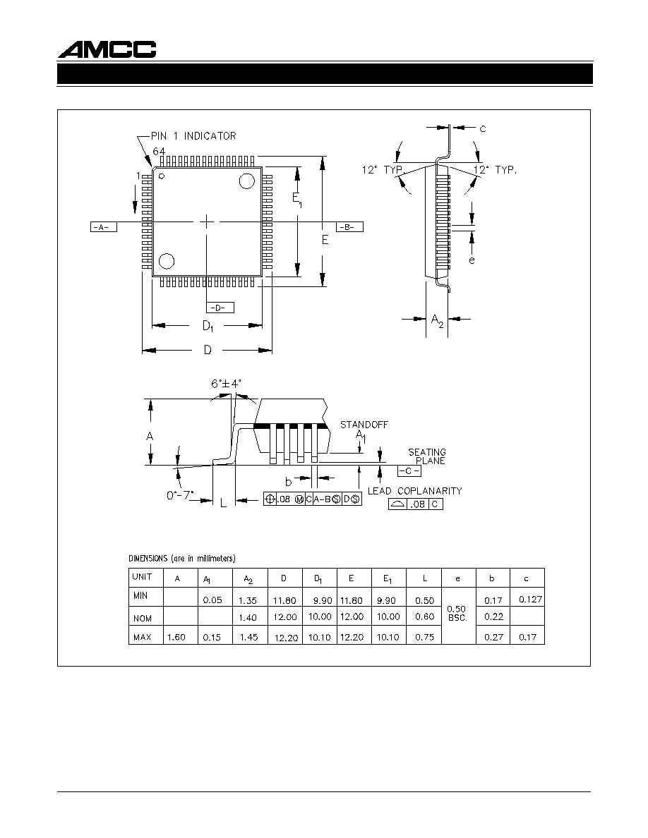
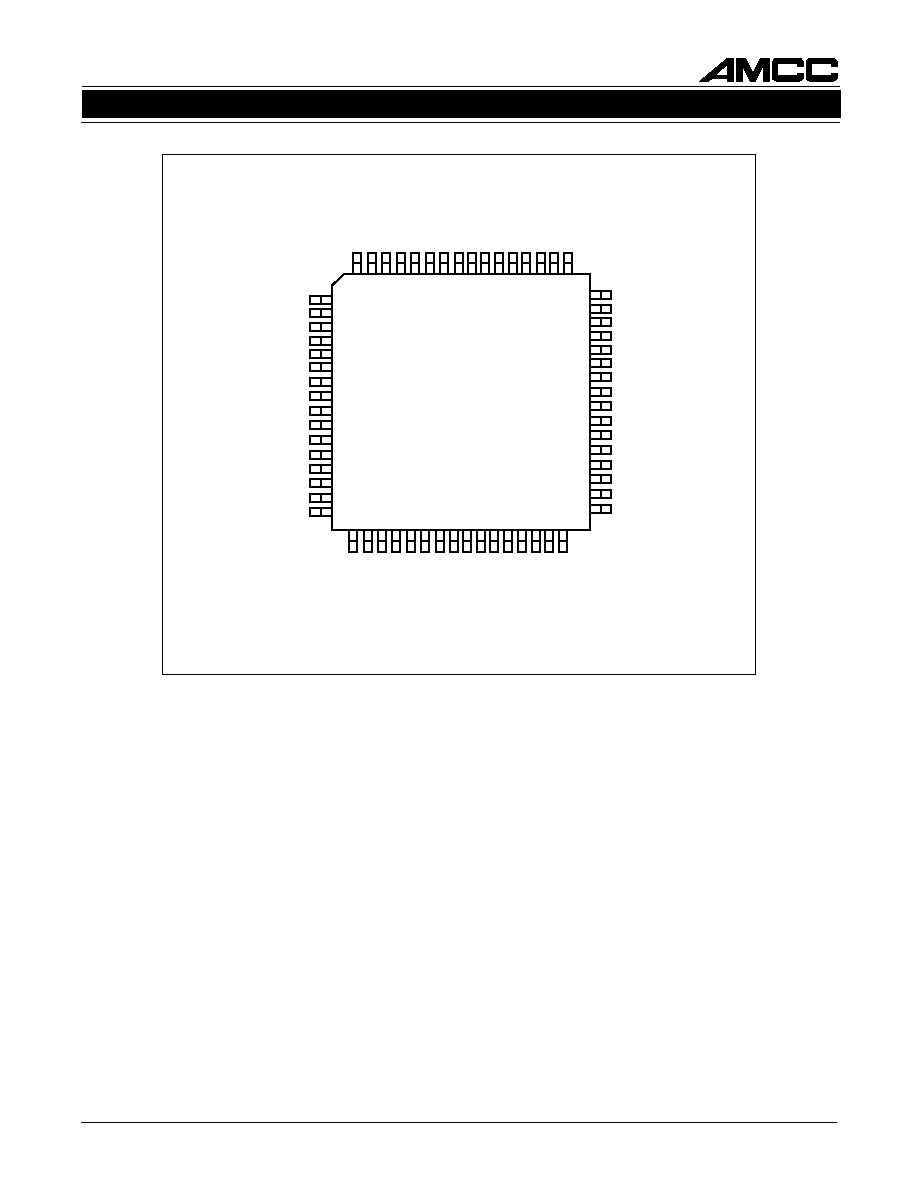
Figure 5. S3029 64 TQFP Package
7
S3029
SONET/SDH/ATM 155 MBIT/S QUAD TRANSCEIVER
February 19, 1999 / Revision B
Figure 6. S3029 64 TQFP Pinout
1
2
3
4
5
6
7
8
9
10
11
19
20
21
22
23
24
25
26
27
28
29
62
61
60
59
58
57
56
55
54
53
52
48
47
46
45
44
43
42
41
40
39
38
S3029
37
36
TXoPOW
TXoGRD
SERCLKOP0
SERCLKON0
SERDATOP0
SERDATON0
CRUoPOW0
CRUoGRD0
SERDATOP1
SERDATON1
SERCLKOP1
SERCLKON1
CRUoPOW1
35
34
33
CRUoGRD1
CRUoPOW2
CRUoGRD2
17
18
ACRUGRD3
LOCKDET3
SERDATIN3
SERDATIP3
SERCLKON3
SERCLKoP3
SERDATON3
SERDATOP3
CRUoGRD3
CRUoPOW3
SERDATON2
LOCKDET2
ACRUPOW3
30
31
32
SERDATOP2
SERCLKON2
SERCLKOP2
64
63
OPAVCC
OPAGRD
LCKREFN2
LCKREFN3
VCOVCC
VCOGRD
SD0
SD1
REFCKINN
REFCKINP
SD2
LCKREFN0
LCKREFN1
51
50
49
SD3
TXCLKOP
TXCLKON
12
13
SERDATIP0
SERDATIN0
TSTCLKEN
ACRUPOW0
ACRUGRD0
REFSEL
SERDATIP1
SERDATIN1
LOCKDET0
ACRUPOW1
ACRUGRD1
ACRUPOW2
ACRUGRD2
14
15
16
LOCKDET1
SERDATIP2
SERDATIN2
TOP VIEW

8
S3029
SONET/SDH/ATM 155 MBIT/S QUAD TRANSCEIVER
February 19, 1999 / Revision B
Performance Specifications
r
e
t
e
m
a
r
a
P
n
i
M
p
y
T
x
a
M
s
t
i
n
U
n
o
i
t
i
d
n
o
C
O
C
V
l
a
n
i
m
o
N
y
c
n
e
u
q
e
r
F
r
e
t
n
e
C
2
5
.
5
5
1
z
H
M
k
c
o
l
C
e
c
n
e
r
e
f
e
R
e
c
n
a
r
e
l
o
T
y
c
n
e
u
q
e
r
F
0
2
-
0
0
1
-
0
2
+
0
0
1
+
m
p
p
m
p
p
t
i
m
s
n
a
r
T
3
-
C
O
T
E
N
O
S
r
o
F
e
c
n
a
r
e
l
o
T
y
c
n
e
u
q
e
r
F
t
i
m
s
n
a
r
T
M
T
A
s
/
t
i
b
M
5
5
1
r
o
F
e
c
n
a
r
e
l
o
T
y
c
n
e
u
q
e
r
F
3
-
S
T
S
/
3
-
C
O
e
g
n
a
R
e
r
u
t
p
a
C
1
e
g
n
a
R
k
c
o
L
t
u
p
t
u
O
k
c
o
l
C
e
l
c
y
C
y
t
u
D
0
4
±
m
p
p
0
0
2
%
2
1
-
,
8
+
0
6
I
U
f
o
%
e
c
n
e
r
e
f
e
r
d
e
x
i
f
o
t
t
c
e
p
s
e
r
h
t
i
W
y
c
n
e
u
q
e
r
f
e
m
i
T
k
c
o
L
n
o
i
t
i
s
i
u
q
c
A
1
3
-
S
T
S
/
3
-
C
O
4
6
µ
c
e
s
p
u
d
e
r
e
w
o
p
y
d
a
e
r
l
a
e
c
i
v
e
d
h
t
i
W
.
K
L
C
F
E
R
d
il
a
v
d
n
a
k
c
o
l
C
e
c
n
e
r
e
f
e
R
e
l
c
y
C
y
t
u
D
t
u
p
n
I
0
3
0
7
f
o
%
d
o
i
r
e
p
&
e
s
i
R
k
c
o
l
C
e
c
n
e
r
e
f
e
R
s
e
m
i
T
ll
a
F
0
.
2
s
n
e
d
u
t
il
p
m
a
f
o
%
0
9
o
t
%
0
1
&
e
s
i
R
t
u
p
t
u
O
L
C
E
P
s
e
m
i
T
ll
a
F
5
.
1
s
n
0
5
,
%
0
9
o
t
%
0
1
V
2
-
C
C
V
o
t
p
a
c
f
p
5
,
d
a
o
l
t
n
e
l
a
v
i
u
q
e
N
/
P
O
K
L
C
X
T
n
o
i
t
a
r
e
n
e
G
r
e
t
t
i
J
5
4
0
.
7
0
.
p
p
.
I
.
U
F
:
1
-
M
T
S
3
F
,
z
H
K
5
6
=
4
z
H
M
3
.
1
=
.
I
.
U
5
1
.
0
=
t
i
m
il
c
e
p
s
H
D
S
/
T
E
N
O
S
1 Guaranteed but not tested.

9
S3029
SONET/SDH/ATM 155 MBIT/S QUAD TRANSCEIVER
February 19, 1999 / Revision B
Recommended Operating Conditions
Absolute Maximum Ratings
r
e
t
e
m
a
r
a
P
n
i
M
p
y
T
x
a
M
t
i
n
U
)
l
a
i
r
t
s
u
d
n
i
(
s
a
i
B
r
e
d
n
u
e
r
u
t
a
r
e
p
m
e
T
t
n
e
i
b
m
A
0
4
-
5
8
+
C
∞
)
l
a
i
c
r
e
m
m
o
c
(
s
a
i
B
r
e
d
n
u
e
r
u
t
a
r
e
p
m
e
T
t
n
e
i
b
m
A
0
0
7
+
C
∞
s
a
i
B
r
e
d
n
u
e
r
u
t
a
r
e
p
m
e
T
n
o
i
t
c
n
u
J
0
1
-
0
3
1
+
C
∞
D
N
G
o
t
t
c
e
p
s
e
R
h
t
i
w
C
C
V
n
o
e
g
a
t
l
o
V
4
1
.
3
3
.
3
6
4
.
3
V
n
i
P
t
u
p
n
I
L
T
T
y
n
A
n
o
e
g
a
t
l
o
V
0
.
0
C
C
V
V
n
i
P
t
u
p
n
I
L
C
E
P
y
n
A
n
o
e
g
a
t
l
o
V
2
-
C
C
V
C
C
V
V
0
5
(
t
n
e
r
r
u
C
e
c
r
u
o
S
t
u
p
t
u
O
L
C
E
P
)
V
2
-
c
c
V
o
t
4
1
5
2
A
m
t
n
e
r
r
u
C
y
l
p
p
u
S
C
C
I
5
2
2
6
7
2
A
m
r
e
t
e
m
a
r
a
P
n
i
M
p
y
T
x
a
M
t
i
n
U
s
a
i
B
r
e
d
n
u
e
r
u
t
a
r
e
p
m
e
T
e
s
a
C
5
5
-
5
2
1
+
C
∞
s
a
i
B
r
e
d
n
u
e
r
u
t
a
r
e
p
m
e
T
n
o
i
t
c
n
u
J
5
5
-
0
5
1
+
C
∞
e
r
u
t
a
r
e
p
m
e
T
e
g
a
r
o
t
S
5
6
-
0
5
1
+
C
∞
D
N
G
o
t
t
c
e
p
s
e
R
h
t
i
w
C
C
V
n
o
e
g
a
t
l
o
V
5
.
0
-
0
.
7
+
V
n
i
P
t
u
p
n
I
L
T
T
y
n
a
n
o
e
g
a
t
l
o
V
5
.
0
-
5
.
5
+
V
n
i
P
t
u
p
n
I
L
C
E
P
y
n
a
n
o
e
g
a
t
l
o
V
0
.
2
-
C
C
V
C
C
V
V
t
n
e
r
r
u
C
k
n
i
S
t
u
p
t
u
O
L
T
T
0
2
A
m
t
n
e
r
r
u
C
e
c
r
u
o
S
t
u
p
t
u
O
L
T
T
0
1
A
m
t
n
e
r
r
u
C
e
c
r
u
o
S
t
u
p
t
u
O
L
C
E
P
d
e
e
p
S
h
g
i
H
0
5
A
m
e
g
a
t
l
o
V
e
g
r
a
h
c
s
i
D
c
i
t
a
t
S
0
0
5
V

10
S3029
SONET/SDH/ATM 155 MBIT/S QUAD TRANSCEIVER
February 19, 1999 / Revision B
TTL Input/Output DC Characteristics
1
1. These conditions will be met with no airflow.
2. When not used, tie the positive differential PECL pin to V
CC
and the negative differential PECL pin to ground via a 3.9K resistor.
(T
A
= -40
∞
C to +85
∞
C, V
CC
= 3.3 V
±
5%)
PECL Output Loading
Recommended Termination of Differential
PECL Signals
PECL Input/Output DC Characteristics
1,2
(T
A
= -40
∞
C to +85
∞
C, V
CC
= 3.3V
±
5%)
2. These input levels provide a zero≠noise immunity and should only be tested in a static, noise-free environment.
Symbol
Parameter
Test Conditions
Min
Max
Unit
VIL
2
VIH
2
IIL
IIH
II
IOS
VIK
VOL
VOH
Input LOW Voltage
Input HIGH Voltage
Input LOW Current
Input HIGH Current
Input HIGH Current at Max VCC
Output Short Circuit Current
Input Clamp Diode Voltage
TTL Output LOW Voltage
TTL Output HIGH Voltage
Guaranteed Input LOW Voltage for all inputs
VCC = MAX, VIN = 0.5V
VCC = MAX, VIN = 2.7V
VCC = MAX, VIN = 3.5V
VCC = MAX, VOUT = 0.5V
VCC = MIN, IIN = -18.0mA
VCC = MIN, IOL = 2mA
VCC = MIN, IOH = -.10mA
2.0
-400.0
-50.0
2.2
0.8
50.0
1.0
-5.0
0.5
Volts
Volts
uA
uA
mA
mA
Volts
Volts
-1.2
Volts
Guaranteed Input HIGH Voltage for all inputs
Symbol
VIL
VIH
VIL
VIH
VOL
VOH
VOD
VID
IIHD
IILD
Input LOW Voltage
Input HIGH Voltage
Input LOW Voltage
Input HIGH Voltage
Output LOW Voltage
Output HIGH Voltage
Guaranteed Input LOW Voltage
for single-ended inputs
Guaranteed Input HIGH Voltage
for single-ended inputs
Guaranteed Input LOW Voltage
for differential inputs
Guaranteed Input HIGH Voltage
for differential inputs
400 ohm termination to GND
400 ohm termination to GND
Differential Output Voltage
Differential Input Voltage
VID = 500mV
VID = 500mV
-0.500
-0.500
0.390
0.200
0.500
VCC -2.000
VCC -1.225
VCC -1.441
VCC -0.570
VCC -2.000
VCC -0.700
VCC -1.750
VCC -0.450
VCC -2.000
VCC -1.300
VCC -1.110
VCC -0.670
Volts
Volts
Volts
Volts
Volts
Volts
Volts
Volts
µ
A
µ
A
20.000
20.000
4
4
1.400
1.000
Output Diff. Voltage
Input Diff. Voltage
Diff. Input High Current
Diff. Input Low Current
IIH
SD Inputs have internal 1K to GND
load resistor.
SD Inputs have internal 1K to GND
load resistor.
mA
Single-ended input High Current
IIL
mA
Single-ended input LOW Current
Parameter
Min
Typ
Max
Unit
Conditions
400
400
100
400

11
S3029
SONET/SDH/ATM 155 MBIT/S QUAD TRANSCEIVER
February 19, 1999 / Revision B
X XXXX XX
Prefix Device Package
Ordering Information
AMCC is a registered trademark of Applied Micro Circuits Corporation.
Copyright Æ 1999 Applied Micro Circuits Corporation
AMCC reserves the right to make changes to its products or to discontinue any semiconductor product or service without notice, and
advises its customers to obtain the latest version of relevant information to verify, before placing orders, that the information being relied
on is current.
AMCC does not assume any liability arising out of the application or use of any product or circuit described herein, neither does it convey
any license under its patent rights nor the rights of others.
AMCC reserves the right to ship devices of higher grade in place of those of lower grade.
AMCC SEMICONDUCTOR PRODUCTS ARE NOT DESIGNED, INTENDED, AUTHORIZED, OR WARRANTED TO BE SUITABLE FOR
USE IN LIFE-SUPPORT APPLICATIONS, DEVICES OR SYSTEMS OR OTHER CRITICAL APPLICATIONS.
Applied Micro Circuits Corporation ∑ 6290 Sequence Dr., San Diego, CA 92121
Phone: (619) 450-9333 ∑ (800) 755-2622 ∑ Fax: (619) 450-9885
http://www.amcc.com
C
E
R T I F I E
D
IS
O 9001
X
I
F
E
R
P
E
C
I
V
E
D
E
G
A
K
C
A
P
t
i
u
c
r
i
C
d
e
t
a
r
g
e
t
n
I
-
S
9
2
0
3
P
F
Q
T
4
6
≠
A