 | –≠–ª–µ–∫—Ç—Ä–æ–Ω–Ω—ã–π –∫–æ–º–ø–æ–Ω–µ–Ω—Ç: S3035 | –°–∫–∞—á–∞—Ç—å:  PDF PDF  ZIP ZIP |
1
S3037
SONET/SDH/ATM OC-3/12 TRANSCEIVER W/CDR
December 10, 1999 / Revision C
BiCMOS LVPECL CLOCK GENERATOR
Æ
DEVICE
SPECIFICATION
SONET/SDH/ATM OC-12 TRANSMITTER AND RECEIVER
S3037
FEATURES
∑ Complies with Bellcore and ITU-T
specifications for jitter tolerance, jitter transfer,
and jitter generation
∑ On-chip high-frequency PLLs for clock
generation and clock recovery
∑ Supports 155.52 Mbit/s (OC-3) and 622.08
Mbit/s (OC-12)
∑ Selectable reference frequencies of 19.44
or 77.76 MHz
∑ Interface to both LVPECL and LVTTL logic
∑ Simple interface with 3.3 V or 5 V optical
modules
∑ Directly compatible with 3.3 V or 5 V network
interface devices
∑ 8-bit LVTTL data path
∑ Compact 10 mm 64 PQFP package
∑ Diagnostic loopback mode
∑ Low jitter LVPECL serial interface
∑ Single 3.3 V supply
APPLICATIONS
∑ SONET/SDH-based transmission systems
∑ SONET/SDH modules
∑ SONET/SDH test equipment
∑ ATM over SONET/SDH
∑ Section repeaters
∑ Add Drop Multiplexers (ADM)
∑ Broad-band cross-connects
∑ Fiber optic terminators
∑ Fiber optic test equipment
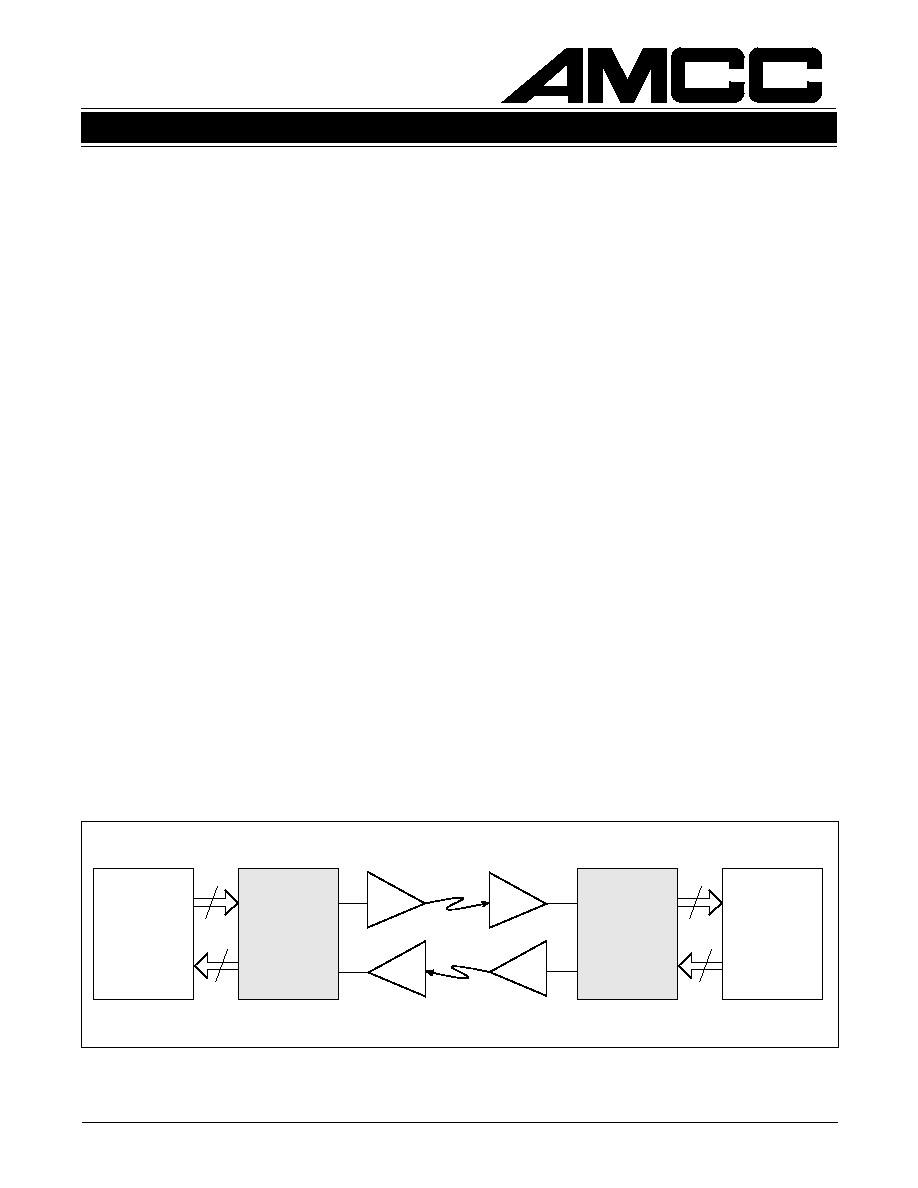
Figure 1. System Block Diagram
SONET/SDH/ATM OC-3/12 TRANSCEIVER W/CDR
S3037
GENERAL DESCRIPTION
The S3037 SONET/SDH transceiver chip is a fully
integrated serialization/deserialization SONET OC-12
(622.08 Mbit/s) and OC-3 (155.52 Mbit/s) interface de-
vice. The chip performs all necessary serial-to-parallel
and parallel-to-serial functions in conformance with
SONET/SDH transmission standards. The device is
suitable for SONET-based ATM applications. Figure
1 shows a typical network application.
On-chip clock synthesis is performed by the high-
frequency phase-locked loop on the S3037
transceiver chip allowing the use of a slower external
transmit clock reference. Clock recovery is performed
on the device by synchronizing its on-chip VCO directly
to the incoming data stream. The S3037 also per-
forms SONET/SDH frame detection. The chip can be
used with a 19.44 or 77.76 MHz reference clock, in
support of existing system clocking schemes.
The low jitter LVPECL interface guarantees compli-
ance with the bit-error rate requirements of the
Bellcore and ITU-T standards. The S3037 is pack-
aged in a 10 mm 64 PQFP, offering designers a small
package outline.
S3037
SONET/SDH
Transceiver
Network
Interface
Processor
Network
Interface
Processor
S3037
SONET/SDH
Transceiver
OTX
ORX
OTX
ORX
8
8
8
8

2
S3037
SONET/SDH/ATM OC-3/12 TRANSCEIVER W/CDR
December 10, 1999 / Revision C
SONET OVERVIEW
Synchronous Optical Network (SONET) is a stan-
dard for connecting one fiber system to another at
the optical level. SONET, together with the Synchro-
nous Digital Hierarchy (SDH) administered by the
ITU-T, forms a single international standard for fiber
interconnect between telephone networks of differ-
ent countries. SONET is capable of accommodating
a variety of transmission rates and applications.
The SONET standard is a layered protocol with four
separate layers defined. These are:
∑ Photonic
∑ Section
∑ Line
∑ Path
Figure 2 shows the layers and their functions. Each
of the layers has overhead bandwidth dedicated to
administration and maintenance. The photonic layer
simply handles the conversion from electrical to opti-
cal and back with no overhead. It is responsible for
transmitting the electrical signals in optical form over
the physical media. The section layer handles the
transport of the framed electrical signals across the
optical cable from one end to the next. Key functions
of this layer are framing, scrambling, and error moni-
toring. The line layer is responsible for the reliable
transmission of the path layer information stream
carrying voice, data, and video signals. Its main
functions are synchronization, multiplexing, and reli-
able transport. The path layer is responsible for the
actual transport of services at the appropriate signal-
ing rates.
Data Rates and Signal Hierarchy
Table 1 contains the data rates and signal designations
of the SONET hierarchy. The lowest level is the basic
SONET signal referred to as the synchronous transport
signal level-1 (STS-1). An STS-
N signal is made up
of
N byte-interleaved STS-1 signals. The optical
counterpart of each STS-
N signal is an optical carrier
level-
N signal (OC-N). The S3037 chip supports OC-3
and OC-12 rates (155.52 and 622.08 Mbit/s).
Frame and Byte Boundary Detection
The SONET/SDH fundamental frame format for
STS-12 consists of 36 transport overhead bytes fol-
lowed by Synchronous Payload Envelope (SPE)
bytes. This pattern of 36 overhead and 1044 SPE bytes
is repeated nine times in each frame. Frame and byte
boundaries are detected using the A1 and A2 bytes
found in the transport overhead. (See Figure 3.)
For more details on SONET operations, refer to the
Bellcore SONET standard document.
Elec.
Optical Data Rate (Mbit/s)
STS-1
OC-1
51.84
STS-3
STM-1
OC-3
155.52
STS-12
STM-4
OC-12
622.08
STS-24
STM-8
OC-24
1244.16
STS-48 STM-16
OC-48 2488.32
End Equipment
End Equipment
Payload to
SPE mapping
Maintenance,
protection,
switching
Optical
transmission
Scrambling,
framing
Fiber Cable
Section layer
Section layer
Photonic layer
Photonic layer
Line layer
Line layer
Path layer
Path layer
Layer Overhead
(Embedded Ops
Channel)
Functions
192 Kbps
0 Kbps
576 Kbps
Table 1. SONET Signal Hierarchy
Figure 2. SONET Structure
Figure 3. STS≠12/OC≠12 Frame Format
9 Rows
12 A1
Bytes
12 A2
Bytes
A1 A1
A1 A1
A2 A2
A2 A2
Transport Overhead 36 Columns
36 x 9 = 324 bytes
Synchronous Payload Envelope 1044 Columns
1044 x 9 = 9396
125
µ
sec
v
v

3
S3037
SONET/SDH/ATM OC-3/12 TRANSCEIVER W/CDR
December 10, 1999 / Revision C
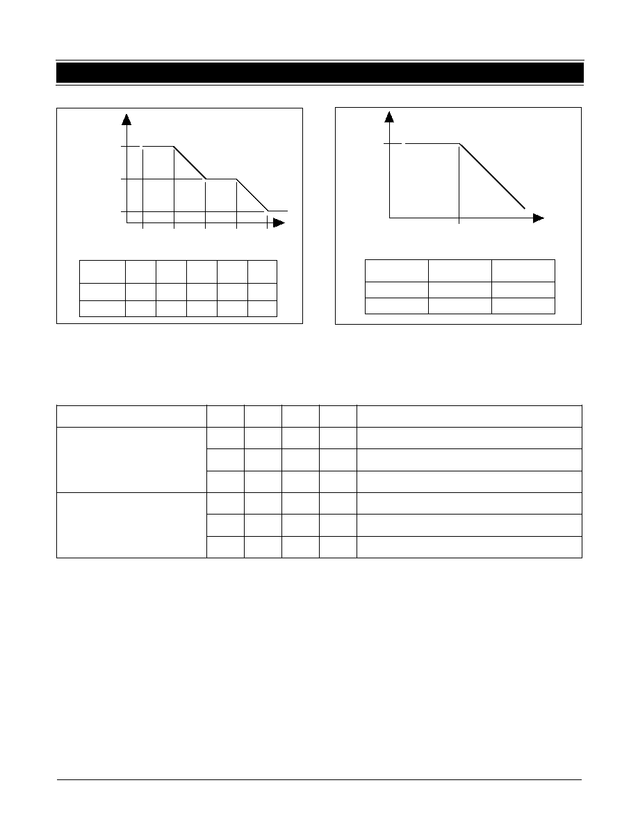
CHARACTERISTICS
Performance
The S3037 PLL complies with the jitter specifications
proposed for SONET/SDH equipment defined by the
T1X1.6/91-022 document, when used as specified.
Jitter Transfer
Jitter transfer function is defined as the ratio of jitter
on the output OC-N/STS-N signal to the jitter applied
on the input OC-N/STS-N signal versus frequency.
Jitter transfer requirements are shown in Figure 5.
The measurement condition is that input sinusoidal
jitter up to the mask level in Figure 4 be applied for
each of the OC-N/STS-N rates.
Input Jitter Tolerance
Input jitter tolerance is defined as the peak to peak
amplitude of sinusoidal jitter applied on the input sig-
nal that causes an equivalent 1 dB optical/electrical
power penalty. SONET input jitter tolerance require-
ments are shown in Figure 4. S3037 performance is
shown in Table 2.
Jitter Generation
The jitter of the serial data outputs shall not exceed
0.01 UI rms when a serial data input with less than
14 ps (OC-12) or 56 ps (OC-3) rms jitter is presented
to the serial data inputs.
S3037 OVERVIEW
The S3037 transceiver implements SONET/SDH se-
rialization/deserialization, transmission, and frame
detection/recovery functions. The block diagram in
Figure 6 shows the basic operation of the chip. This
chip can be used to implement the front end of
SONET equipment, which consists primarily of the
serial transmit interface and the serial receive inter-
face. The chip handles all the functions of these two
elements, including parallel-to-serial and serial-to-par-
allel conversion, clock generation and recovery, and
system timing. The system timing circuitry consists
of management of the data stream, framing, and
clock distribution throughout the front end.
The S3037 is divided into a transmitter section and a
receiver section. The sequence of operations is as
follows:
Transmitter Operations:
1. 8-bit parallel input
2. Parallel-to-serial conversion
3. Serial output
Receiver Operations:
1. Clock and data recovery from serial input
2. Frame detection
3. Serial-to-parallel conversion
4. 8-bit parallel output
Internal clocking and control functions are transpar-
ent to the user. Details of data timing can be seen in
Figures 10 through 15.
The S3037 supports clock recovery for the OC-12/
STM-4 or OC-3/STM-1 data rates. Differential serial
data is input to the chip at the specified rate and
clock recovery is performed on the incoming data
stream. A reference clock is required to minimize the
PLL lock time and provide a stable output clock
source in the absence of serial input data. Retimed
data and clock are output from the S3037.
AMCC CONGO
(S1201) POS/ATM SONET Mapper
AMCC NILE
(S1202) ATM SONET Mapper
Suggested Interface Devices
4
S3037
SONET/SDH/ATM OC-3/12 TRANSCEIVER W/CDR
December 10, 1999 / Revision C
Figure 4. Input Jitter Tolerance Specification
f0
f1
f2
f3
ft
0.15
1.5
15
Sinusodal
Input Jitter
Amplitude
(UI p-p)
Frequency
OC/STS
Level
f0
(Hz)
f2
(Hz)
f3
(kHz)
ft
(kHz)
f1
(Hz)
12
10
30
300
25
250
3
10
30
300
6.5
65
Figure 5. Jitter Transfer Specification
fc
P
Jitter
Transfer
Frequency
Acceptable
Range
slope = -20 dB/decade
OC/STS
Level
fc
(kHz)
P
(dB)
12
1,2
500
0.1
3
1,2
130
0.1
1. Bellcore Specifications: TR-NWT-000253, Issue 2,
December 1991.
2. CCITT Recommendations: G.958.
Table 2. Jitter Tolerance
r
e
t
e
m
a
r
a
P
n
i
M
p
y
T
x
a
M
s
t
i
n
U
s
n
o
i
t
i
d
n
o
C
e
c
n
a
r
e
l
o
T
r
e
t
t
i
J
2
1
-
S
T
S
4
.
0
5
6
.
0
I
U
z
H
M
5
<
f
<
z
H
k
0
5
2
5
.
1
4
I
U
z
H
k
5
2
<
f
<
z
H
0
0
3
5
1
0
2
I
U
z
H
0
3
<
f
<
z
H
0
1
e
c
n
a
r
e
l
o
T
r
e
t
t
i
J
3
-
S
T
S
4
.
0
8
.
0
I
U
z
H
M
3
.
1
<
f
<
z
H
k
5
6
5
.
1
5
I
U
z
H
k
5
.
6
<
f
<
z
H
0
0
3
5
1
2
2
I
U
z
H
0
3
<
f
<
z
H
0
1

5
S3037
SONET/SDH/ATM OC-3/12 TRANSCEIVER W/CDR
December 10, 1999 / Revision C
1:8 SERIAL
TO PARALLEL
TIMING
GEN
CLOCK AND DATA
RECOVERY
RSTB
RSDP/N
FRAME
BYTE
DETECT
DLEB
OOF
FP
POUT[7:0]
8
BACKUP
REFERENCE
GEN
POCLK
8
PIN[7:0]
8:1 PARALLEL
TO SERIAL
TSDP/N
PICLK
TIMING
GEN
PCLK
CLOCK
SYNTHESIZER
RSTB
D
MODE 0
MODE 1
TXCAP1
TXCAP2
Transmitter
Receiver
LLEB
SLPTIME
REFCLKP/N
TTLREF
SDPECL
TESTEN
RXCAP1
RXCAP2
0
1
1
0
1
0
RSTB
RSTB
RSTB
1
0
1
0
0
1
0
1
Figure 6. S3037 Transceiver Functional Block Diagram