 | –≠–ª–µ–∫—Ç—Ä–æ–Ω–Ω—ã–π –∫–æ–º–ø–æ–Ω–µ–Ω—Ç: S3040B | –°–∫–∞—á–∞—Ç—å:  PDF PDF  ZIP ZIP |

1
S3041
SONET/SDH/ATM OC-48 8:1 TRANSMITTER
January 7, 2000 / Revision G
BiCMOS LVPECL CLOCK GENERATOR
Æ
DEVICE
SPECIFICATION
SONET/SDH/ATM OC-12 TRANSMITTER AND RECEIVER
S3041
FEATURES
∑ Micro-power Bipolar technology
∑ Complies with Bellcore and ITU-T
specifications
∑ On-chip high-frequency PLL for clock generation
∑ Supports 2.488 GHz (OC-48)
∑ Reference frequency of 155.52 MHz
∑ 8-bit LVDS data path
∑ Compact 100 TQFP/TEP package
∑ Diagnostic loopback mode
∑ Line loopback
∑ Lock detect
∑ Low jitter LVPECL interface
∑ Single 3.3V supply
APPLICATIONS
∑ SONET/SDH-based transmission systems
∑ SONET/SDH modules
∑ SONET/SDH test equipment
∑ ATM over SONET/SDH
∑ Section repeaters
∑ Add drop multiplexers
∑ Broad-band cross-connects
∑ Fiber optic terminators
∑ Fiber optic test equipment
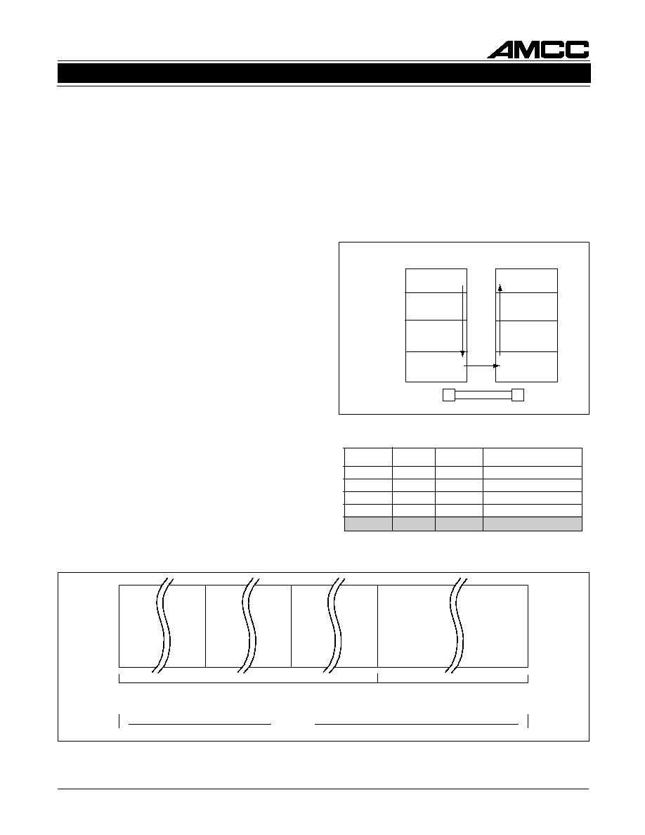
Figure 1. System Block Diagram
SONET/SDH/ATM OC-48 8:1 TRANSMITTER
S3041
GENERAL DESCRIPTION
The S3041 SONET/SDH Mux chip is a fully integrated
serialization SONET OC-48 (2.488 GHz) interface de-
vice. The chip performs all necessary parallel-to-serial
and clock synthesis functions in conformance with
SONET/SDH transmission standards. The device is
suitable for SONET-based ATM applications. Figure
1 shows a typical network application.
On-chip clock synthesis PLL components are con-
tained in the S3041 Mux chip allowing the use of a
slower external transmit clock reference. The chip
can be used with a 155.52 MHz reference clock, in
support of existing system clocking schemes.
The low jitter LVPECL interface guarantees compli-
ance with the bit-error rate requirements of the
Bellcore and ITU-T standards. The S3041 is pack-
aged in a 100 TQFP/TEP, offering designers a small
package outline.
Network Interface
Processor
S3045
S3041
S3042
S3042
S3041
OTX
ORX
OTX
ORX
8
8
8
8
8
8
8
8
8
8
8
8
8
8
8
8
8
8
8
8
Network Interface
Processor
S3045
S3040
S3040

2
S3041
SONET/SDH/ATM OC-48 8:1 TRANSMITTER
January 7, 2000 / Revision G
The sequence of operations is as follows:
Transmitter Operations:
1. 8-bit parallel input
2. Parallel-to-serial conversion
3. Serial output
Internal clocking and control functions are transpar-
ent to the user. Details of data timing can be seen in
Figures 7 through 10.
S3041 OVERVIEW
The S3041 Mux implements SONET/SDH serializa-
tion and transmission functions. The block diagram
in Figure 2 shows basic operation of the chip. This
chip can be used to implement the front end of
SONET equipment, which consists primarily of the
serial transmit interface and the serial receive inter-
face. The chip includes parallel-to-serial conversion
and system timing. The system timing circuitry con-
sists of a high-speed phase detector, clock dividers,
and clock distribution throughout the front end.
Figure 2. S3041 Functional Block Diagram
AMCC
S3040
OC-48 Clock Recovery Device
AMCC
S3045
OC-48 to OC-12 Demux
AMCC
S3042
OC-48 Demux
Suggested Interface Devices
M
U
X
M
U
X
16
PINP/N[7:0]
LLDP/N
LLCLKP/N
LLEB
8:1 PARALLEL
TO SERIAL
TSDP/N
LSDP/N
DLEB
PICLKP/N
TIMING
GEN
PCLKP/N
LOCKDET
VCO,
CLOCK DIVIDER and
PHASE DETECTOR
RSTB
D
TSCLKP/N
LSCLKP/N
TESTEN
REFCLKP/N
READP/N
PULSE0P/N
77MCK
KILLTXCLKN
CAP1/2
FIFO
3
S3041
SONET/SDH/ATM OC-48 8:1 TRANSMITTER
January 7, 2000 / Revision G
SONET OVERVIEW
Synchronous Optical Network (SONET) is a standard
for connecting one fiber system to another at the opti-
cal level. SONET, together with the Synchronous
Digital Hierarchy (SDH) administered by the ITU-T,
forms a single international standard for fiber inter-
connect between telephone networks of different
countries. SONET is capable of accommodating a
variety of transmission rates and applications.
The SONET standard is a layered protocol with four
separate layers defined. These are:
∑ Photonic
∑ Section
∑ Line
∑ Path
Figure 3 shows the layers and their functions. Each
of the layers has overhead bandwidth dedicated to
administration and maintenance. The photonic layer
simply handles the conversion from electrical to optical
and back with no overhead. It is responsible for
transmitting the electrical signals in optical form over
the physical media. The section layer handles the
transport of the framed electrical signals across the
optical cable from one end to the next. Key functions
of this layer are framing, scrambling, and error moni-
toring. The line layer is responsible for the reliable
transmission of the path layer information stream
carrying voice, data, and video signals. Its main
functions are synchronization, multiplexing, and reli-
able transport. The path layer is responsible for the
actual transport of services at the appropriate signaling
rates.
Figure 4 shows a standard OC-48 Frame former
structure.
Data Rates and Signal Hierarchy
Table 1 contains the data rates and signal designations
of the SONET hierarchy. The lowest level is the basic
SONET signal referred to as the synchronous transport
signal level-1 (STS-1). An STS-
N signal is made up of
N byte-interleaved STS-1 signals. The optical counter-
part of each STS-
N signal is an optical carrier level-N
signal (OC-
N). The S3041 chip supports OC-48 rate
(2.488 Gbps).
Elec.
CCITT
Optical Data Rate (Mbps)
STS-1
OC-1
51.84
STS-3
STM-1
OC-3
155.52
STS-12
STM-4
OC-12
622.08
STS-24
STM-8
OC-24
1244.16
STS-48 STM-16
OC-48 2488.32
Table 1. SONET Signal Hierarchy
Figure 3. SONET Structure
Figure 4. STS≠48/OC≠48 Frame Format
End Equipment
Payload to
SPE mapping
Maintenance,
protection,
switching
Optical
transmission
Scrambling,
framing
Fiber Cable
End Equipment
Section layer
Photonic layer
Line layer
Path layer
Path layer
Section layer
Photonic layer
Line layer
Functions
9 Rows
48 A1
Bytes
48 A2
Bytes
A1 A1
A1 A1
A2 A2
A2 A2
Transport Overhead 144 Columns
144 x 9 = 1296 bytes
Synchronous Payload Envelope 4176 Columns
4176 x 9 = 37,584 bytes
125
µ
sec
s
s

4
S3041
SONET/SDH/ATM OC-48 8:1 TRANSMITTER
January 7, 2000 / Revision G
S3041 ARCHITECTURE/FUNCTIONAL
DESIGN
Mux Operation
The S3041 performs the serializing stage in the pro-
cessing of a transmit SONET STS-48 bit serial data
stream. It converts the byte serial 311 Mbyte/sec data
stream to bit serial format at 2.488 Gbps. Diagnostic
loopback is provided (transmitter to receiver), and Line
Loopback is also provided (receiver to transmitter).
A high-frequency bit clock is generated from a
155.52 MHz frequency reference by using a fre-
quency synthesizer consisting of an on-chip
phase-locked loop circuit with a divider.
Clock Divider and Phase Detector
The Clock Divider and Phase Detector, shown in the
block diagram in Figure 2, contains monolithic PLL
components.
The REFCLK input must be generated from a differ-
ential LVPECL crystal oscillator which has a
frequency accuracy of better than 20 ppm in order
for the VCOCLK frequency to have the same accu-
racy required for operation in a SONET system.
In order to meet the .01 UI SONET jitter specifica-
tions, the maximum reference clock jitter must be
guaranteed over the 12 KHz to 20 MHz bandwidth.
For details of reference clock jitter requirements, see
Table 2.
Timing Generator
The Timing Generator function, seen in Figure 2, pro-
vides two separate functions. It provides a byte rate
version of the TSCLK, and a mechanism for aligning
the phase between the incoming byte clock and the
clock which loads the parallel-to-serial shift register.
The PCLK output is a byte rate version of TSCLK.
For STS-48, the PCLK frequency is 311 MHz. PCLK
is intended for use as a byte speed clock for up-
stream multiplexing and overhead processing circuits.
Using PCLK for upstream circuits will ensure a
stable frequency and phase relationship between the
data coming into and leaving the S3041 device.
In the parallel-to-serial conversion process, the in-
coming data is passed from the PICLK byte clock
timing domain to the internally generated byte clock
timing domain, which is phase aligned to TSCLK.
The Timing Generator also produces a feedback ref-
erence clock to the Phase Detector. A counter divides
the synthesized clock down to the same frequency
as the reference clock REFCLK.
Parallel-to-Serial Converter
The FIFO is used to accomodate phase differences
between the internal byte clock and the external
PICLK. The READ and PULSE signals are used to
control the FIFO to prevent overflow/underflow con-
ditions.
The Parallel-to-Serial converter shown in Figure 2 is
comprised of a FIFO and a parallel-to-serial register.
The FIFO latches the data from the PIN[7:0] bus on
the rising edge of PICLK. The parallel-to-serial regis-
ter is a parallel loadable shift register which takes its
parallel input from the FIFO.
An internally generated byte clock, which is phase
aligned to the transmit serial clock as described in the
Timing Generator description, activates the parallel
data transfer between registers. The serial data is
shifted out of the second register at the TSCLK rate.
Table 2. Reference Jitter Limits
r
e
t
t
i
J
k
c
o
l
C
e
c
n
e
r
e
f
e
R
m
u
m
i
x
a
M
d
n
a
B
z
H
M
0
2
o
t
z
H
k
2
1
n
i
g
n
i
t
a
r
e
p
O
e
d
o
M
s
m
r
s
p
1
8
4
-
S
T
S

5
S3041
SONET/SDH/ATM OC-48 8:1 TRANSMITTER
January 7, 2000 / Revision G
e
m
a
N
n
i
P
l
e
v
e
L
O
/
I
#
n
i
P
n
o
i
t
p
i
r
c
s
e
D
7
P
N
I
P
7
N
N
I
P
6
P
N
I
P
6
N
N
I
P
5
P
N
I
P
5
N
N
I
P
4
P
N
I
P
4
N
N
I
P
3
P
N
I
P
3
N
N
I
P
2
P
N
I
P
2
N
N
I
P
1
P
N
I
P
1
N
N
I
P
0
P
N
I
P
0
N
N
I
P
S
D
V
L
I
9
2
0
3
1
3
2
3
3
3
4
3
5
3
6
3
7
3
8
3
9
3
0
4
1
4
2
4
3
4
4
4
K
L
C
I
P
e
h
t
o
t
d
e
n
g
il
a
,
d
r
o
w
c
e
s
/
e
t
y
b
M
1
1
3
A
.
t
u
p
n
I
a
t
a
D
l
e
ll
a
r
a
P
t
i
b
t
n
a
c
i
f
i
n
g
i
s
t
s
o
m
e
h
t
s
i
>
7
<
N
I
P
.
k
c
o
l
c
t
u
p
n
i
l
e
l
l
a
r
a
p
.
)
d
e
t
t
i
m
s
n
a
r
t
t
i
b
t
s
r
i
f
e
h
t
,
d
r
o
w
M
C
P
h
c
a
e
f
o
1
t
i
b
o
t
g
n
i
d
n
o
p
s
e
r
r
o
c
(
h
c
a
e
f
o
8
t
i
b
o
t
g
n
i
d
n
o
p
s
e
r
r
o
c
(
t
i
b
t
n
a
c
i
f
i
n
g
i
s
t
s
a
e
l
e
h
t
s
i
>
0
<
N
I
P
e
h
t
n
o
d
e
l
p
m
a
s
s
i
>
0
:
7
<
N
I
P
.
)
d
e
t
t
i
m
s
n
a
r
t
t
i
b
t
s
a
l
e
h
t
,
d
r
o
w
M
C
P
.
K
L
C
I
P
f
o
e
g
d
e
g
n
i
s
i
r
P
K
L
C
I
P
N
K
L
C
I
P
S
D
V
L
I
7
4
8
4
t
u
p
n
i
e
l
c
y
c
y
t
u
d
%
0
5
y
ll
a
n
i
m
o
n
z
H
M
1
1
3
A
.
k
c
o
l
C
t
u
p
n
I
l
e
ll
a
r
a
P
e
h
t
r
e
f
s
n
a
r
t
o
t
d
e
s
u
s
i
K
L
C
I
P
.
d
e
n
g
il
a
s
i
>
0
:
7
<
N
I
P
h
c
i
h
w
o
t
,
k
c
o
l
c
-
o
t
-
l
e
ll
a
r
a
p
e
h
t
n
i
r
e
t
s
i
g
e
r
g
n
i
d
l
o
h
a
o
t
n
i
s
t
u
p
n
i
N
I
P
e
h
t
n
o
a
t
a
d
.
>
0
:
7
<
N
I
P
s
e
l
p
m
a
s
K
L
C
I
P
f
o
e
g
d
e
g
n
i
s
i
r
e
h
T
.
r
e
t
r
e
v
n
o
c
l
a
i
r
e
s
P
D
L
L
N
D
L
L
y
ll
a
n
r
e
t
x
E
d
e
s
a
i
B
.
f
f
i
D
L
C
E
P
V
L
I
8
5
7
5
n
o
i
n
a
p
m
o
c
a
m
o
r
f
d
e
d
i
v
o
r
p
y
ll
a
m
r
o
n
s
t
u
p
n
I
.
a
t
a
D
k
c
a
b
p
o
o
L
e
n
i
L
n
i
n
o
i
t
c
n
u
f
k
c
a
b
p
o
o
l
e
n
i
l
a
t
n
e
m
e
l
p
m
i
o
t
d
e
s
U
.
e
c
i
v
e
d
2
4
0
3
S
d
e
t
a
r
e
n
e
g
e
r
e
r
a
s
l
a
n
g
i
s
k
c
o
l
c
d
n
a
a
t
a
d
l
a
i
r
e
s
e
v
i
e
c
e
r
e
h
t
h
c
i
h
w
.
r
e
t
t
i
m
s
n
a
r
t
1
4
0
3
S
e
h
t
h
g
u
o
r
h
t
d
e
s
s
a
p
d
n
a
P
K
L
C
L
L
N
K
L
C
L
L
y
ll
a
n
r
e
t
x
E
d
e
s
a
i
B
.
f
f
i
D
L
C
E
P
V
L
I
2
6
1
6
n
o
i
n
a
p
m
o
c
a
m
o
r
f
d
e
d
i
v
o
r
p
y
ll
a
m
r
o
n
s
t
u
p
n
I
.
k
c
o
l
C
k
c
a
b
p
o
o
L
e
n
i
L
n
i
n
o
i
t
c
n
u
f
k
c
a
b
p
o
o
l
e
n
i
l
a
t
n
e
m
e
l
p
m
i
o
t
d
e
s
U
.
e
c
i
v
e
d
2
4
0
3
S
d
e
t
a
r
e
n
e
g
e
r
e
r
a
s
l
a
n
g
i
s
k
c
o
l
c
d
n
a
a
t
a
d
l
a
i
r
e
s
e
v
i
e
c
e
r
e
h
t
h
c
i
h
w
.
r
e
t
t
i
m
s
n
a
r
t
1
4
0
3
S
e
h
t
h
g
u
o
r
h
t
d
e
s
s
a
p
d
n
a
P
K
L
C
F
E
R
N
K
L
C
F
E
R
y
ll
a
n
r
e
t
n
I
d
e
s
a
i
B
.
f
f
i
D
L
C
E
P
V
L
I
0
8
1
8
k
c
o
l
ll
i
w
t
i
u
c
r
i
c
r
o
t
a
r
e
n
e
g
k
c
o
l
c
e
h
T
.
z
H
M
2
5
.
5
5
1
.
k
c
o
l
C
e
c
n
e
r
e
f
e
R
n
a
h
t
i
w
K
L
C
F
E
R
e
h
t
g
n
i
r
a
p
m
o
c
y
b
k
c
o
l
c
e
c
n
e
r
e
f
e
r
s
i
h
t
o
t
.
k
c
o
l
c
n
w
o
d
d
e
d
i
v
i
d
y
ll
a
n
r
e
t
n
i
B
E
L
D
L
T
T
V
L
I
5
6
s
t
c
e
l
e
s
,
e
v
i
t
c
a
n
e
h
W
.
w
o
L
e
v
i
t
c
A
.
e
l
b
a
n
E
k
c
a
b
p
o
o
L
c
i
t
s
o
n
g
a
i
D
)
K
L
C
S
T
(
k
c
o
l
c
d
n
a
)
D
S
T
(
a
t
a
d
y
r
a
m
i
r
p
e
h
T
.
k
c
a
b
p
o
o
l
c
i
t
s
o
n
g
a
i
d
,
k
c
o
l
c
k
c
a
b
p
o
o
l
c
i
t
s
o
n
g
a
i
d
e
h
t
,
e
v
i
t
c
a
n
e
h
W
.
e
v
i
t
c
a
s
y
a
w
l
a
e
r
a
.
e
v
i
t
c
a
e
r
a
s
t
u
p
t
u
o
)
D
S
L
(
a
t
a
d
d
n
a
,
)
K
L
C
S
L
(
B
T
S
R
L
T
T
V
L
I
4
6
,
t
e
s
e
r
g
n
i
r
u
D
.
w
o
l
e
v
i
t
c
a
,
e
c
i
v
e
d
e
h
t
r
o
f
t
u
p
n
i
t
e
s
e
R
.
t
e
s
e
R
r
e
t
s
a
M
.
e
l
g
g
o
t
t
o
n
s
e
o
d
K
L
C
P
B
E
L
L
L
T
T
V
L
I
8
6
n
e
h
w
k
c
a
b
p
o
o
L
e
n
i
L
s
t
c
e
l
e
S
.
w
o
L
e
v
i
t
c
A
.
e
l
b
a
n
E
k
c
a
b
p
o
o
L
e
n
i
L
m
o
r
f
a
t
a
d
e
h
t
e
t
u
o
r
ll
i
w
1
4
0
3
S
e
h
t
,
e
v
i
t
c
a
s
i
B
E
L
L
n
e
h
W
.
e
v
i
t
c
a
r
o
f
e
v
i
t
c
a
n
I
.
s
t
u
p
t
u
o
K
L
C
S
T
/
D
S
T
e
h
t
o
t
s
t
u
p
n
i
K
L
C
L
L
/
D
L
L
e
h
t
.
n
o
i
t
a
r
e
p
o
l
a
m
r
o
n
Table 3. Input Pin Assignment and Description