 | –≠–ª–µ–∫—Ç—Ä–æ–Ω–Ω—ã–π –∫–æ–º–ø–æ–Ω–µ–Ω—Ç: S3067 | –°–∫–∞—á–∞—Ç—å:  PDF PDF  ZIP ZIP |

1
S3067
MULTIRATE (OC-48/24/12/3/GBE) SONET/SDH/ATM TRANSCEIVER WITH FEC
October 26, 2000 / Revision A
BiCMOS LVPECL CLOCK GENERATOR
Æ
DEVICE
SPECIFICATION
SONET/SDH/ATM OC-12 TRANSMITTER AND RECEIVER
S3067
FEATURES
∑ SiGe BiCMOS technology
∑ Complies with Bellcore and ITU-T
specifications
∑ On-chip high-frequency PLL for clock
generation
∑ Supports OC-48 (with FEC),
OC-24 (with FEC),
OC-12 (with FEC),
OC-3 (with FEC)
∑ FEC capability of up to 8 bytes per
255-byte block
∑ Reference frequency of 155.52 to 178 MHz
∑ Interface to LVPECL and TTL logic
∑ 16 Bit single-ended LVPECL data path
∑ Compact 156 TBGA package
∑ Diagnostic loopback mode
∑ Supports line timing
∑ Lock Detect
∑ Signal detect input
∑ Low jitter LVPECL interface
∑ Internal FIFO to decouple transmit clocks
∑ Single 3.3 V supply
∑ Typical power 1.5 W
APPLICATIONS
∑ Wavelength Division Multiplexing equipment
∑ SONET/SDH-based transmission systems
∑ SONET/SDH modules
∑ SONET/SDH test equipment
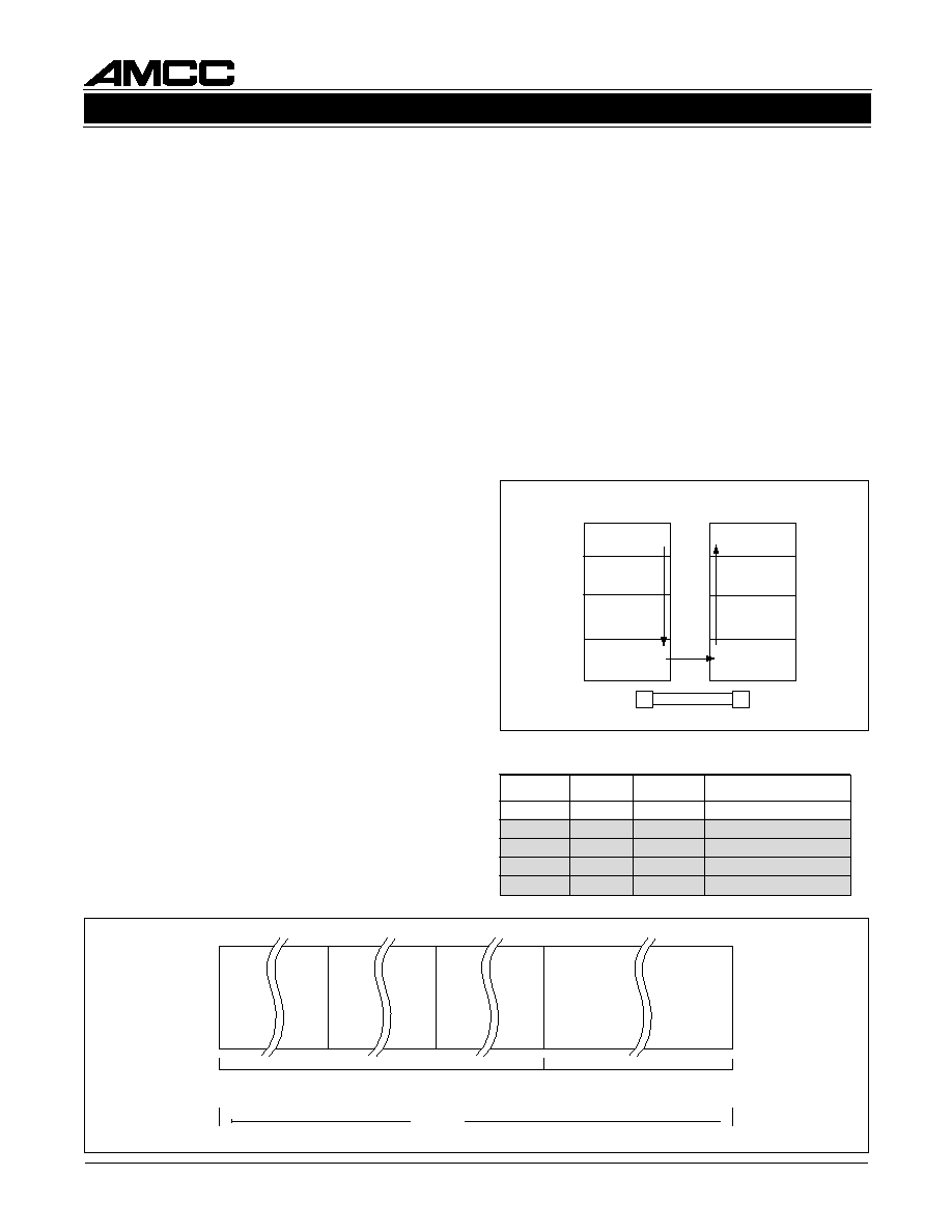
Figure 1. System Block Diagram
MULTIRATE (OC-48/24/12/3/GBE) SONET/SDH/ATM TRANSCEIVER WITH FEC
S3067
∑ ATM over SONET/SDH
∑ Section repeaters
∑ Add Drop Multiplexers (ADM)
∑ Broad-band cross-connects
∑ Fiber optic terminators
∑ Fiber optic test equipment
GENERAL DESCRIPTION
The S3067 SONET/SDH transceiver chip is a fully
integrated multirate serialization/deserialization
SONET OC-48, OC-24, OC-12 and OC-3 interface
device. The chip performs all necessary serial-to-
parallel and parallel-to-serial functions in
conformance with SONET/SDH transmission and
Forward Error Correction (FEC) standards. The de-
vice is suitable for SONET-based WDM applications.
Figure 1 shows a typical network application.
On-chip clock synthesis is performed by the high-
frequency phase-locked loop on the S3067
transceiver chip allowing the use of a slower external
transmit clock reference. The chip can be used with a
155.52 to 178 MHz reference clock, in support of
existing system clocking schemes.
The low jitter LVPECL interface guarantees compliance
with the bit-error rate requirements of the Bellcore
and ITU-T standards. The S3067 is packaged in a 156
TBGA, offering designers a small package outline.
The S3067 supports FEC designs with internal divid-
ers or external clocking modes.
S3076
Clock
Recovery
Unit
S3062
Receive
S3062
Transmit
FEC Added
S3067
Transmit
Serialization
S3067
Receive
Deserialization
S3076
Clock
Recovery
Unit
S3062
Receive
FEC Data
Stripped Off
S3062
Transmit
S3067
Transmit
Serialization
S3067
Receive
Deserialization
2.488 Gbps
X
2.488
Gbps
155 Mbps
X
X
2.67 Gbps
X + Y
167 Mbps
X + Y
167 Mbps
X + Y
155 Mbps
X
X + Y
2.67 Gbps
2.488 Gbps
X
PERFORMANCE MONITOR
PERFORMANCE MONITOR
X = Data
Y = FEC Data
E/O
O/E
OPTICAL FIBER
2
S3067
MULTIRATE (OC-48/24/12/3/GBE) SONET/SDH/ATM TRANSCEIVER WITH FEC
October 26, 2000/ Revision A
SONET OVERVIEW
Synchronous Optical Network (SONET) is a standard
for connecting one fiber system to another at the opti-
cal level. SONET, together with the Synchronous
Digital Hierarchy (SDH) administered by the ITU-T,
forms a single international standard for fiber inter-
connect between telephone networks of different
countries. SONET is capable of accommodating a
variety of transmission rates and applications.
The SONET standard is a layered protocol with four
separate layers defined. These are:
∑ Photonic
∑ Section
∑ Line
∑ Path
Figure 2 shows the layers and their functions. Each
of the layers has overhead bandwidth dedicated to
administration and maintenance. The photonic layer
simply handles the conversion from electrical to optical
and back with no overhead. It is responsible for
transmitting the electrical signals in optical form over
the physical media. The section layer handles the
transport of the framed electrical signals across the
optical cable from one end to the next. Key functions
of this layer are framing, scrambling, and error moni-
toring. The line layer is responsible for the reliable
transmission of the path layer information stream
carrying voice, data, and video signals. Its main
functions are synchronization, multiplexing, and reli-
able transport. The path layer is responsible for the
actual transport of services at the appropriate signaling
rates.
Data Rates and Signal Hierarchy
Table 1 contains the data rates and signal designations
of the SONET hierarchy. The lowest level is the basic
SONET signal referred to as the synchronous transport
signal level-1 (STS-1). An STS-
N signal is made up of
N byte-interleaved STS-1 signals. The optical counter-
part of each STS-
N signal is an optical carrier level-N
signal (OC-
N). The S3067 chip supports up to the OC-
48 rate with different FEC modes.
Frame and Byte Boundary Detection
The SONET/SDH fundamental frame format for
STS-48 consists of 144 transport overhead bytes
followed by Synchronous Payload Envelope (SPE)
bytes. This pattern of 144 overhead and 4176 SPE
bytes is repeated nine times in each frame. Frame and
byte boundaries are detected using the A1 and A2
bytes found in the transport overhead. (See Figure 3.)
For more details on SONET operations, refer to the
Bellcore SONET standard document.
Elec.
CCITT
Optical Data Rate (Mbit/s)
STS-1
OC-1
51.84
STS-3
STM-1
OC-3
155.52
STS-12
STM-4
OC-12
622.08
STS-24
STM-8
OC-24
1244.16
STS-48 STM-16
OC-48 2488.32
Table 1. SONET Signal Hierarchy
Figure 2. SONET Structure
Figure 3. STS≠48/OC≠48 Frame Format
9 Rows
48 A1
Bytes
48 A2
Bytes
A1 A1
A1 A1
A2 A2
A2 A2
Transport Overhead 144 Columns
144 x 9 = 1296 bytes
Synchronous Payload Envelope 4176 Columns
4176 x 9 = 37,584 bytes
125
µ
sec
s
s
End Equipment
Payload to
SPE mapping
Maintenance,
protection,
switching
Optical
transmission
Scrambling,
framing
Fiber Cable
End Equipment
Section layer
Photonic layer
Line layer
Path layer
Path layer
Section layer
Photonic layer
Line layer
Functions

3
S3067
MULTIRATE (OC-48/24/12/3/GBE) SONET/SDH/ATM TRANSCEIVER WITH FEC
October 26, 2000 / Revision A
S3067 OVERVIEW
The S3067 transceiver implements SONET/SDH
and WDM serialization/deserialization, and transmis-
sion functions. The block diagram in Figure 4 shows
the basic operation of the chip. This chip can be
used to implement the front end of WDM equipment,
which consists primarily of the serial transmit inter-
face and the serial receive interface. The chip
handles all the functions of these two elements, in-
cluding parallel-to-serial and serial-to-parallel
conversion, clock generation, and system timing.
The system timing circuitry consists of management
of the data stream and clock distribution throughout
the front end.
S3067 has ability to bypass the internal VCO with an
external source and also with the receive clock. The
device generates 14/15, 15/14, 16/17 and 17/16
clocks based upon the received clock and an exter-
nal clock to incorporate the FEC capability. The
dividers support the first two rates shown in Table 4.
The S3067 is divided into a transmitter section and a
receiver section. The sequence of operations is as
follows:
0
L
E
S
E
T
A
R
1
L
E
S
E
T
A
R
e
d
o
M
g
n
i
t
a
r
e
p
O
0
0
3
-
C
O
0
1
2
1
-
C
O
1
0
E
B
G
/
4
2
-
C
O
1
1
8
4
-
C
O
Table 2. Data Rate Select
Transmitter Operations:
1. 16-bit parallel input
2. Parallel-to-serial conversion
3. Serial output
Receiver Operations:
1. Serial input
2. Serial-to-parallel conversion
3. 16-bit parallel output
Internal clocking and control functions are transpar-
ent to the user.
S3067 Supports six different code rates, besides the
normal rate, for each of the four operating modes.
y
t
i
l
i
b
a
p
a
C
g
n
i
t
c
e
r
r
o
C
r
o
r
r
E
g
n
i
w
o
h
s
e
t
a
R
e
d
o
C
e
u
d
n
o
i
s
n
a
p
x
E
h
t
d
i
w
d
n
a
B
B
S
F
&
s
d
r
o
w
e
d
o
c
o
t
k
c
o
l
c
t
u
p
n
i
d
e
s
a
e
r
c
n
i
f
o
e
l
p
m
a
x
E
)
z
H
M
(
6
1
-
M
T
S
/
8
4
-
S
T
S
r
o
f
y
c
n
e
u
q
e
r
f
k
c
o
l
b
e
t
y
b
-
5
5
2
r
e
p
s
e
t
y
b
8
e
s
a
e
r
c
n
i
%
4
1
.
7
=
8
3
2
/
5
5
2
3
6
.
6
6
1
=
4
1
/
5
1
*
2
5
.
5
5
1
=
8
3
2
/
5
5
2
*
2
5
.
5
5
1
k
c
o
l
b
e
t
y
b
-
5
5
2
r
e
p
s
e
t
y
b
7
e
s
a
e
r
c
n
i
%
5
2
.
6
=
0
4
2
/
5
5
2
4
2
.
5
6
1
=
6
1
/
7
1
*
2
5
.
5
5
1
=
0
4
2
/
5
5
2
*
2
5
.
5
5
1
k
c
o
l
b
e
t
y
b
-
5
5
2
r
e
p
s
e
t
y
b
6
e
s
a
e
r
c
n
i
%
7
3
.
5
=
2
4
2
/
5
5
2
7
8
.
3
6
1
=
2
4
2
/
5
5
2
*
2
5
.
5
5
1
k
c
o
l
b
e
t
y
b
-
5
5
2
r
e
p
s
e
t
y
b
5
e
s
a
e
r
c
n
i
%
1
5
.
4
=
4
4
2
/
5
5
2
3
5
.
2
6
1
=
4
4
2
/
5
5
2
*
2
5
.
5
5
1
k
c
o
l
b
e
t
y
b
-
5
5
2
r
e
p
s
e
t
y
b
4
e
s
a
e
r
c
n
i
%
6
6
.
3
=
6
4
2
/
5
5
2
1
2
.
1
6
1
=
2
8
/
5
8
*
2
5
.
5
5
1
=
6
4
2
/
5
5
2
*
2
5
.
5
5
1
k
c
o
l
b
e
t
y
b
-
5
5
2
r
e
p
s
e
t
y
b
3
e
s
a
e
r
c
n
i
%
2
8
.
2
=
8
4
2
/
5
5
2
1
9
.
9
5
1
=
8
4
2
/
5
5
2
*
2
5
.
5
5
1
Table 4. FEC Modes
Table 3. FEC Select
0
C
E
F
1
2
O
C
V
r
e
d
i
v
i
D
K
L
C
S
R
r
e
d
i
v
i
D
0
0
1
7
1
6
1
1
0
1
6
1
7
1
0
1
1
5
1
4
1
1
1
1
4
1
5
1
0
0
0
7
1
X
1
0
0
6
1
X
0
1
0
5
1
X
1
1
0
4
1
X
C
C
M
A
6
7
0
3
S
e
c
i
v
e
D
y
r
e
v
o
c
e
R
k
c
o
l
C
8
4
-
C
O
C
C
M
A
2
6
0
3
S
r
o
t
i
n
o
M
e
c
n
a
m
r
o
f
r
e
P
8
4
-
C
O
Suggested Interface Devices

4
S3067
MULTIRATE (OC-48/24/12/3/GBE) SONET/SDH/ATM TRANSCEIVER WITH FEC
October 26, 2000/ Revision A
Figure 4. S3067 Transceiver Functional Block Diagram
CLOCKS
LOCKDET
155MCKP/N
19MCK
PCLKP/N
PHERR
TSDP/N
TSCLKP/N
OVREF
POUT[15:0]
POCLKP/N
TIMGEN
16:1
PARALLEL
TO SERIAL
CLOCK
SYNTHESIZER
D
TXDP/N
TXCLKP/N
POCLK (Internal)
REFCLKP/N
PICLKP/N
TXDP/N
(Internal)
TXCLKP/N
(Internal)
RSCLKP/N
DLEB
SQUELCH
IVREF
RSTB
SDLVPECL
SDTTL
RSDP/N
KILLRXCLK
LLEB
PIN[15:0]
BYPASS
TESTEN
CAP2
CAP1
RLPTIME
FECSEL2
PHINIT
D
D
D
1:16
SERIAL TO
PARALLEL
TIMGEN
R
3
16
16
RATESEL[0:1]
FECSEL[2:0]
BYPASSCLKP/N
N
SLPTIME
VCO CLOCK
TX
RX
2

5
S3067
MULTIRATE (OC-48/24/12/3/GBE) SONET/SDH/ATM TRANSCEIVER WITH FEC
October 26, 2000 / Revision A
Figure 5. Clock Synthesizer
M
N
PD
LPF
VCO
VCOCLK
REFCLK
FECSEL (0-1)
FECSEL 2
RSCLK
Where N = 14/15/16/17
M = 14/15/16/17
RSCLK N
VCOCLK M
RSCLK Divider
VCO Divider
=
A high on FECSEL2 selects RSCLK divided by N. A low on FECSEL2 selects the REFCLK. The REFCLK or
RSCLK divided by N is divided by 1/M (multiplied by M) in the loop. The value of M and N can be selected by
FECSEL0 and FECSEL1.
When FECSEL2 = 0, VCOCLK = REFCLK * M. The user must select the proper value of REFCLK and M to get
the desired VCOCLK frequency. When FECSEL2 = 1, VCOCLK = (RSCLK * M)
˜
N. The user must select the
proper M/N ratio (with FECSEL0 and FECSEL1) to get the desired VCOCLK value. (See Tables 3 and 4.)
Example: OC-48 FEC capability of 8 bytes per 255-byte block. Required VCOCLK = 2.6656 GHz.
Method 1:
Required VCOCLK = 2.6656 GHz
FECSEL2 = 0, selects REFCLK
FECSEL0 = 1 and FECSEL1 = 0, selects VCO divider(M) = 16
REFCLK = 2.6656 GHz
˜
16 = 166.60 MHz
VCOCLK = REFCLK
˜
(1/M) = 166.60 * 16 = 2.6656 GHz
Method 2:
Required VCOCLK = 2.6656 GHz
FECSEL2 = 1, selects RSCLK
FECSEL0 = 0 and FECSEL1 = 0, selects VCO divider(M) = 17 and RSCLK divider(N) = 16
RSCLK = (2.6656 * 16)
˜
17 = 2.5088 GHz
VCOCLK = RSCLK
˜
N
˜
(1/M) = 2.5088 GHz
˜
16 * 17 = 2.6656 GHz.

6
S3067
MULTIRATE (OC-48/24/12/3/GBE) SONET/SDH/ATM TRANSCEIVER WITH FEC
October 26, 2000/ Revision A
S3067 TRANSCEIVER
FUNCTIONAL DESCRIPTION
TRANSMITTER OPERATION
The S3067 transceiver chip performs the serializa-
tion stage in the processing of a transmit SONET
STS-48/STS-24/STS-12/STS-3/GBE data stream
depending on the data rate selected. It converts 16
bit parallel data to bit serial format.
A high-frequency bit clock can be generated from a
155.52 to 178 MHz frequency reference by using an
integral frequency synthesizer consisting of a phase-
locked loop circuit with a divider in the loop.
Diagnostic loopback (transmitter to receiver) and line
loopback (receiver to transmitter) is provided. See
other operating modes.
The bypass signal selects between the BYPASSCLK
and the VCO clock. BYPASSCLK can be used to
provide an alternative clock to the internal VCO
when the user selects an error correcting capability
which is not provided by the S3067 dividers. The
user must provide the required frequency for the
BYPASSCLK when error correcting capability of 6/5/
4/3 bytes per 255-byte block is selected.
Clock Synthesizer
The clock synthesizer, shown in the block diagram in
Figures 4 and 5, is a monolithic PLL that generates
the serial output clock frequency locked to the input
Reference Clock (REFCLKP/N).
The REFCLKP/N input must be generated from a
crystal oscillator which has a frequency accuracy of
better than the value stated in Table 10 in order for
the TSCLK frequency to have the same accuracy
required for operation in a SONET system. Lower
accuracy crystal oscillators may be used in applica-
tions less demanding than SONET/SDH.
The on-chip PLL consists of a phase detector, which
compares the phase relationship between the VCO
output and the REFCLKP/N input, a loop filter which
converts the phase detector output into a smooth DC
voltage, and a VCO, whose frequency is varied by
this voltage.
The divide by 'N' and divide by 'M' provide the
counters required to support error correcting capabil-
ity. The values of 'N' and 'M' can be selected by
FECSEL lines.
The loop filter generates a VCO control voltage
based on the average DC level of the phase discrimi-
nator output pulses. A single external clean-up
capacitor is utilized as part of the loop filter. The loop
filter's corner frequency is optimized to minimize out-
put phase jitter.
Timing Generator
The timing generation function, seen in Figure 4,
provides a divide-by-16 version of the transmit serial
clock. This circuitry also provides an internally generated
load signal, which transfers the PIN[15:0] data from
the parallel input register to the serial shift register.
The PCLK output is a divide-by-16 rate version of
transmit serial clock (divide-by-16). PCLK is in-
tended for use as a divide-by-16 clock for upstream
multiplexing and overhead processing circuits. Using
PCLK for upstream circuits will ensure a stable fre-
quency and phase relationship between the data
coming into and leaving the S3067 device.
The timing generator also produces a feedback ref-
erence clock to the clock synthesizer. A counter
divides the synthesized clock down to the same fre-
quency as the reference clock REFCLK. The PLL in
the clock synthesizer maintains the stability of the
synthesized clock by comparing the phase of the
internal clock with that of the Reference Clock
(REFCLK).
Table 5. Reference Jitter Limits
e
d
o
M
g
n
i
t
a
r
e
p
O
h
t
d
i
W
d
n
a
B
r
e
t
t
i
J
S
M
R
8
4
-
S
T
S
z
H
M
0
2
o
t
z
H
k
2
1
c
B
d
1
6
-
4
2
-
S
T
S
z
H
M
0
1
o
t
z
H
k
2
1
s
p
2
2
1
-
S
T
S
z
H
M
5
o
t
z
H
k
2
1
s
p
4
3
-
S
T
S
z
H
M
1
o
t
z
H
k
2
1
s
p
6
1

7
S3067
MULTIRATE (OC-48/24/12/3/GBE) SONET/SDH/ATM TRANSCEIVER WITH FEC
October 26, 2000 / Revision A
Parallel-to-Serial Converter
The parallel-to-serial converter shown in Figure 4 is
comprised of a FIFO and a parallel-to-serial register.
The FIFO input latches the data from the PIN[15:0]
bus on the rising edge of PICLK. The parallel-to-
serial register is a loadable shift register which takes
its parallel input from the FIFO output.
An internally generated divide-by-16 clock, which is
phase aligned to the transmit serial clock as de-
scribed in the Timing Generator description, activates
the parallel data transfer between registers. The serial
data is shifted out of the parallel-to-serial register at
the TSCLK rate.
FIFO
A FIFO is added to decouple the internal and exter-
nal (PICLK) clocks. The internally generated
divide-by-16 clock is used to clock out data from the
FIFO. PHINIT and LOCKDET are used to center or
reset the FIFO. The PHINIT and LOCKDET signals
will center the FIFO after the third PICLK pulse. This
is in order to insure that PICLK is stable. This
scheme allows the user to have an infinite PCLK to
PICLK delay through the ASIC. Once the FIFO is
centered, the PCLK to PICLK delay can have a
maximum drift specified by Table 20.
FIFO Initialization
The FIFO can be initialized in one of the following
three ways:
1.During power up, once the PLL has locked to the
reference clock provided on the REFCLK pins, the
LOCKDET will go active and initialize the FIFO.
2.When RSTB goes active, the entire chip is reset.
This causes the PLL to go out of lock and thus the
LOCKDET goes inactive. When the PLL reac-
quires the lock, the LOCKDET goes active and
initializes the FIFO. Note: PCLK is held reset when
RSTB is active.
3.The user can also initialize the FIFO by raising
PHINIT.
During the normal running operation, the incoming
data is passed from the PICLK timing domain to the
internally generated divide by 16 clock timing do-
main. Although the frequency of PICLK and the
internally generated clock is the same, their phase
relationship is arbitrary. To prevent errors caused by
short setup or hold times between the two timing
domains, the timing generator circuitry monitors the
phase relationship between PICLK and the internally
generated clock. When a potential setup or hold time
violation is detected, the phase error goes high.
When PHERR conditions occur, PHINIT should be
activated to recenter the FIFO (at least 2 PCLK peri-
ods). This can be done by connecting PHERR to
PHINIT. When realignment occurs up to 10 bytes of
data will be lost. The user can also take in the
PHERR signal, process it and send an output to
PHINIT in such a way that idle bytes are lost during
the realignment process. PHERR will go inactive
when the realignment is complete.
RECEIVER OPERATION
The S3067 receiver chip provides the first stage of
digital processing of a receive SONET STS-48/STS-
24/STS-12/STS-3/GBE bit-serial stream. The bit
serial data stream is then converted into a 16 bit
half-word data format. A loopback mode is provided
for diagnostic loopback (transmitter to receiver). A
line loopback (receiver to transmitter) is also pro-
vided. Both line and local loopback modes can be
active at the same time.
Serial-to-Parallel Converter
The serial-to-parallel converter consists of two 16-bit
registers. The first is a serial-in, parallel-out shift reg-
ister, which performs the serial-to-parallel conversion
clocked by the clock recovery block. On the falling
edge of the POCLK, the data in the parallel register
is transferred to an output parallel register which
drives POUT[15:0].
OTHER OPERATING MODES
Diagnostic Loopback
When the Diagnostic Loopback Enable (DLEB) input
is low, a loopback from the transmitter to the re-
ceiver at the serial data rate can be set up for
diagnostic purposes. The differential serial output
data from the transmitter is routed to the serial-to-
parallel block in place of the normal data stream
(RSD). TSD/TSCLK outputs are active. DLEB takes
precedence over SDPECL and SDTTL.

8
S3067
MULTIRATE (OC-48/24/12/3/GBE) SONET/SDH/ATM TRANSCEIVER WITH FEC
October 26, 2000/ Revision A
Line Loopback
The line loopback circuitry selects the source of the
data and clock which is output on TSD and TSCLK.
When the Line Loopback Enable input (LLEB) is
high, it selects data and clock from the parallel-to-
serial converter block. When LLEB is low, it forces
the output data multiplexer to select the data and
clock from the RSD and RSCLK inputs, and a re-
ceive-to-transmit loopback can be established at the
serial data rate. Diagnostic loopback and line
loopback can be active at the same time.
Loop Timing
In Serial Loop Timing mode (SLPTIME), the clock
synthesizer PLL of the S3067 is bypassed, and the
timing of the entire transmitter section is controlled
by the Receive Serial Clock, RSCLKP/N. This mode
is entered by setting the SLPTIME input to a TTL
high level.
In this mode the REFCLKP/N input is not used, and
the RATESEL input is ignored for all transmit func-
tions. It should be carefully noted that the internal
PLL continues to operate in this mode, and contin-
ues as the source for the 19MCK and 155MCK, and
if these signals are being used (e.g. as the reference
for an external S3076 clock recovery device), the
REFCLKP/N and RATESEL inputs must be properly
driven.
In Reference Loop Timing mode (RLPTIME), the
Parallel Clock from the receiver (POCLK) is used as
the reference clock to the transmitter. In this mode,
the REFCLKP/N input is not used. The 19MCK and
155MCK are generated from the POCLK in this op-
erating mode. When operating the S3067 in
RLPTIME mode, the 19MCK and 155MCK outputs
should not be used as the back-up reference clock
for a clock and data recovery device (S3066,
S3040). When performing loopback testing (DLEB),
the S3067 must not be in RLPTIME.
"Squelched Clock" Operation
Some integrated optical receiver/clock recovery
modules force their recovered serial receive clock
output to the logic zero state if the optical signal is
removed or reduced below a fixed threshold. This
condition is accompanied by the expected
deassertion of the Signal Detect (SD) output.
The S3067 has been designed for operation with
clock recovery devices that provide continuous serial
clock for seamless downstream clocking in the event
of optical signal loss.
For operation with an optical transceiver that pro-
vides the "squelched clock" behavior as described
above, the S3067 can be operated in the "squelched
clock" mode by activating the SQUELCH pin.
In this condition, the Receive Serial Clock (RSCLKP/N)
is used for all receiver timing when the SDLVPECL/
SDTTL inputs are in the active state. When the
SDLVPECL/SDTTL inputs are placed in the inactive
state (usually by the deassertion of LOCKDET or Sig-
nal Detect from the optical transceiver/clock recovery
unit) the transmitter serial clock will be used to maintain
timing in the receiver section. This will allow the
POCLK to continue to run and the parallel outputs to
flush out the last received characters and then assume
the all zero state imposed at the serial data input.
It is important to note that in this mode there will be
a one time shortening or lengthening of the POCLK
cycle, resulting in an apparent phase shift in the
POCLK at the deassertion of the SD condition. An-
other similar phase shift will occur when the SD
condition is reasserted.
In the normal operating mode with SQUELCH inac-
tive, there will be no phase discontinuities at the
POCLK output during signal loss or reacquisition
(assuming operation with continuous clocking from
the CRU device such as the AMCC S3076).

9
S3067
MULTIRATE (OC-48/24/12/3/GBE) SONET/SDH/ATM TRANSCEIVER WITH FEC
October 26, 2000 / Revision A
Table 6. S3067 Transmitter Pin Assignment and Descriptions
e
m
a
N
n
i
P
l
e
v
e
L
O
/
I
#
n
i
P
n
o
i
t
p
i
r
c
s
e
D
0
N
I
P
1
N
I
P
2
N
I
P
3
N
I
P
4
N
I
P
5
N
I
P
6
N
I
P
7
N
I
P
8
N
I
P
9
N
I
P
0
1
N
I
P
1
1
N
I
P
2
1
N
I
P
3
1
N
I
P
4
1
N
I
P
5
1
N
I
P
e
l
g
n
i
S
d
e
d
n
E
L
C
E
P
V
L
I
2
A
3
B
2
B
3
C
1
A
2
C
1
B
2
D
3
E
1
C
2
E
3
F
2
F
1
E
1
F
3
G
l
e
ll
a
r
a
p
K
L
C
I
P
e
h
t
o
t
d
e
n
g
il
a
,
6
1
-
y
b
-
e
d
i
v
i
d
A
.
t
u
p
n
I
a
t
a
D
l
e
ll
a
r
a
P
o
t
g
n
i
d
n
o
p
s
e
r
r
o
c
(
t
i
b
t
n
a
c
i
f
i
n
g
i
s
t
s
o
m
e
h
t
s
i
]
5
1
[
N
I
P
.
k
c
o
l
c
t
u
p
n
i
e
h
t
s
i
]
0
[
N
I
P
.
)
d
e
t
t
i
m
s
n
a
r
t
t
i
b
t
s
r
i
f
e
h
t
,
d
r
o
w
M
C
P
h
c
a
e
f
o
1
t
i
b
,
d
r
o
w
M
C
P
h
c
a
e
f
o
6
1
t
i
b
o
t
g
n
i
d
n
o
p
s
e
r
r
o
c
(
t
i
b
t
n
a
c
i
f
i
n
g
i
s
t
s
a
e
l
e
g
d
e
g
n
i
s
i
r
e
h
t
n
o
d
e
l
p
m
a
s
s
i
]
0
:
5
1
[
N
I
P
.
)
d
e
t
t
i
m
s
n
a
r
t
t
i
b
t
s
a
l
e
h
t
.
K
L
C
I
P
f
o
P
K
L
C
I
P
N
K
L
C
I
P
y
ll
a
n
r
e
t
n
I
d
e
s
a
i
B
.
f
f
i
D
L
C
E
P
V
L
I
4
A
3
A
e
l
c
y
c
y
t
u
d
%
0
5
y
ll
a
n
i
m
o
n
,
6
1
-
y
b
-
e
d
i
v
i
d
A
.
k
c
o
l
C
t
u
p
n
I
l
e
ll
a
r
a
P
o
t
d
e
s
u
s
i
K
L
C
I
P
.
d
e
n
g
i
l
a
s
i
]
0
:
5
1
[
N
I
P
h
c
i
h
w
o
t
,
k
c
o
l
c
t
u
p
n
i
e
h
t
n
i
r
e
t
s
i
g
e
r
g
n
i
d
l
o
h
a
o
t
n
i
s
t
u
p
n
i
N
I
P
e
h
t
n
o
a
t
a
d
e
h
t
r
e
f
s
n
a
r
t
s
e
l
p
m
a
s
K
L
C
I
P
f
o
e
g
d
e
g
n
i
s
i
r
e
h
T
.
r
e
t
r
e
v
n
o
c
l
a
i
r
e
s
-
o
t
-
l
e
ll
a
r
a
p
.
]
0
:
5
1
[
N
I
P
1
P
A
C
2
P
A
C
g
o
l
a
n
A
I
5
R
5
T
d
n
a
r
o
t
i
c
a
p
a
c
r
e
t
l
i
f
p
o
o
l
l
a
n
r
e
t
x
e
e
h
T
.
r
o
t
i
c
a
p
a
C
r
e
t
l
i
F
p
o
o
L
.
6
2
e
r
u
g
i
F
e
e
S
.
s
n
i
p
e
s
e
h
t
o
t
d
e
t
c
e
n
n
o
c
e
r
a
s
r
o
t
s
i
s
e
r
F
E
R
V
I
C
D
I
4
C
.
e
g
a
t
l
o
v
e
c
n
e
r
e
f
e
r
t
u
p
n
i
L
C
E
P
V
L
d
e
d
n
e
-
e
l
g
n
i
S
T
I
N
I
H
P
e
l
g
n
i
S
d
e
d
n
E
L
C
E
P
V
L
I
2
G
.
g
n
i
m
i
t
l
a
n
r
e
t
n
i
n
g
il
a
e
r
ll
i
w
e
g
d
e
g
n
i
s
i
R
.
n
o
i
t
a
z
il
a
i
t
i
n
I
e
s
a
h
P
P
D
S
T
N
D
S
T
.
f
f
i
D
L
M
C
O
1
1
R
2
1
R
,
s
l
a
n
g
i
s
m
a
e
r
t
s
a
t
a
d
l
a
i
r
e
s
L
M
C
l
a
i
t
n
e
r
e
f
f
i
D
.
a
t
a
D
l
a
i
r
e
S
t
i
m
s
n
a
r
T
.
e
l
u
d
o
m
r
e
t
t
i
m
s
n
a
r
t
l
a
c
i
t
p
o
n
a
o
t
d
e
t
c
e
n
n
o
c
y
ll
a
m
r
o
n
P
K
L
C
S
T
N
K
L
C
S
T
.
f
f
i
D
L
M
C
O
8
R
9
R
d
e
s
u
e
b
n
a
c
N
/
P
K
L
C
S
T
L
M
C
l
a
i
t
n
e
r
e
f
f
i
D
.
k
c
o
l
C
l
a
i
r
e
S
t
i
m
s
n
a
r
T
d
e
t
c
e
l
e
s
e
b
ll
i
w
y
c
n
e
u
q
e
r
f
k
c
o
l
c
s
i
h
T
.
l
a
n
g
i
s
D
S
T
e
h
t
e
m
i
t
e
r
o
t
.
L
E
S
C
E
F
d
n
a
L
E
S
E
T
A
R
y
b
P
K
L
C
P
N
K
L
C
P
.
f
f
i
D
L
C
E
P
V
L
O
6
C
6
B
y
b
k
c
o
l
c
t
i
b
l
a
n
r
e
t
n
i
e
h
t
g
n
i
d
i
v
i
d
y
b
d
e
t
a
r
e
n
e
g
k
c
o
l
c
e
c
n
e
r
e
f
e
r
A
n
e
e
w
t
e
b
s
r
e
f
s
n
a
r
t
e
d
i
w
-
d
r
o
w
e
t
a
n
i
d
r
o
o
c
o
t
d
e
s
u
y
ll
a
m
r
o
n
s
i
t
I
.
6
1
.
e
c
i
v
e
d
7
6
0
3
S
e
h
t
d
n
a
c
i
g
o
l
m
a
e
r
t
s
p
u
R
R
E
H
P
e
l
g
n
i
S
d
e
d
n
E
L
C
E
P
V
L
O
5
A
e
r
e
h
t
h
c
i
h
w
r
o
f
e
l
c
y
c
K
L
C
P
h
c
a
e
g
n
i
r
u
d
h
g
i
H
s
e
s
l
u
P
.
r
o
r
r
E
e
s
a
h
P
l
a
n
r
e
t
n
i
e
h
t
n
e
e
w
t
e
b
n
o
i
t
a
l
o
i
v
g
n
i
m
i
t
d
l
o
h
/
p
u
-
t
e
s
l
a
i
t
n
e
t
o
p
a
s
i
e
h
t
n
o
d
e
t
a
d
p
u
s
i
R
R
E
H
P
.
s
n
i
a
m
o
d
g
n
i
m
i
t
K
L
C
I
P
d
n
a
k
c
o
l
c
e
t
y
b
.
s
t
u
p
t
u
o
K
L
C
P
e
h
t
f
o
e
g
d
e
g
n
il
l
a
f

10
S3067
MULTIRATE (OC-48/24/12/3/GBE) SONET/SDH/ATM TRANSCEIVER WITH FEC
October 26, 2000/ Revision A
Table 7. S3067 Receiver Pin Assignment and Descriptions
e
m
a
N
n
i
P
l
e
v
e
L
O
/
I
#
n
i
P
n
o
i
t
p
i
r
c
s
e
D
P
D
S
R
N
D
S
R
.
f
f
i
D
L
M
C
I
5
1
H
5
1
G
y
ll
a
m
r
o
n
s
l
a
n
g
i
s
m
a
e
r
t
s
a
t
a
D
l
a
i
r
e
S
e
v
i
e
c
e
R
L
M
C
l
a
i
t
n
e
r
e
f
f
i
D
.
e
l
u
d
o
m
r
e
v
i
e
c
e
r
l
a
c
i
t
p
o
n
a
o
t
d
e
t
c
e
n
n
o
c
d
n
a
d
e
s
a
i
b
y
ll
a
n
r
e
t
n
I
.
d
e
t
a
n
i
m
r
e
t
L
C
E
P
V
L
D
S
e
l
g
n
i
S
d
e
d
n
E
L
C
E
P
V
L
I
6
1
N
e
v
i
t
c
A
.
n
w
o
d
-
ll
u
p
l
a
n
r
e
t
n
i
h
t
i
w
L
C
E
P
V
L
.
t
c
e
t
e
D
l
a
n
g
i
S
L
C
E
P
V
L
L
C
E
P
V
L
K
0
1
d
e
d
n
e
-
e
l
g
n
i
s
A
.
0
c
i
g
o
l
t
a
d
l
e
h
s
i
L
T
T
D
S
n
e
h
w
h
g
i
H
o
t
e
l
u
d
o
m
r
e
v
i
e
c
e
r
l
a
c
i
t
p
o
l
a
n
r
e
t
x
e
e
h
t
y
b
n
e
v
i
r
d
e
b
o
t
t
u
p
n
i
s
i
L
C
E
P
V
L
D
S
n
e
h
W
.
r
e
w
o
p
l
a
c
i
t
p
o
d
e
v
i
e
c
e
r
f
o
s
s
o
l
a
e
t
a
c
i
d
n
i
ll
i
w
s
n
i
p
)
N
/
P
D
S
R
(
n
I
a
t
a
D
l
a
i
r
e
S
e
v
i
e
c
e
R
e
h
t
n
o
a
t
a
d
e
h
t
,
e
v
i
t
c
a
n
i
,
e
v
i
t
c
a
s
i
L
C
E
P
V
L
D
S
n
e
h
W
.
o
r
e
z
t
n
a
t
s
n
o
c
a
o
t
d
e
c
r
o
f
y
ll
a
n
r
e
t
n
i
e
b
n
e
h
W
.
y
l
l
a
m
r
o
n
d
e
s
s
e
c
o
r
p
e
b
l
l
i
w
s
n
i
p
N
/
P
D
S
R
e
h
t
n
o
a
t
a
d
d
a
e
t
s
n
i
e
l
u
d
o
m
r
e
v
i
e
c
e
r
l
a
c
i
t
p
o
e
h
t
o
t
d
e
t
c
e
n
n
o
c
e
b
o
t
s
i
L
T
T
D
S
t
n
e
m
e
l
p
m
i
o
t
h
g
i
H
d
e
i
t
e
b
d
l
u
o
h
s
L
C
E
P
V
L
D
S
n
e
h
t
,
L
C
E
P
V
L
D
S
f
o
n
a
t
n
e
m
e
l
p
m
i
o
t
d
e
t
c
e
n
n
o
c
n
u
t
f
e
l
r
o
,
t
c
e
t
e
D
l
a
n
g
i
S
w
o
L
e
v
i
t
c
a
n
a
.
t
c
e
t
e
D
l
a
n
g
i
S
h
g
i
H
e
v
i
t
c
a
L
T
T
D
S
L
T
T
V
L
I
6
1
P
s
i
L
C
E
P
V
L
D
S
n
e
h
w
h
g
i
H
e
v
i
t
c
A
.
t
c
e
t
e
D
l
a
n
g
i
S
L
T
T
V
L
t
a
d
l
e
h
s
i
L
C
E
P
V
L
D
S
n
e
h
w
w
o
L
e
v
i
t
c
A
.
)
0
c
i
g
o
l
(
d
e
t
c
e
n
n
o
c
n
u
l
a
n
r
e
t
x
e
e
h
t
y
b
n
e
v
i
r
d
e
b
o
t
t
u
p
n
i
L
T
T
V
L
d
e
d
n
e
-
e
l
g
n
i
s
A
.
1
c
i
g
o
l
l
a
c
i
t
p
o
d
e
v
i
e
c
e
r
f
o
s
s
o
l
a
e
t
a
c
i
d
n
i
o
t
e
l
u
d
o
m
r
e
v
i
e
c
e
r
l
a
c
i
t
p
o
ll
i
w
s
n
i
p
N
/
P
D
S
R
e
h
t
n
o
a
t
a
d
e
h
t
,
e
v
i
t
c
a
n
i
s
i
L
T
T
D
S
n
e
h
W
.
r
e
w
o
p
,
e
v
i
t
c
a
s
i
L
T
T
D
S
n
e
h
W
.
o
r
e
z
t
n
a
t
s
n
o
c
a
o
t
d
e
c
r
o
f
y
ll
a
n
r
e
t
n
i
e
b
.
y
ll
a
m
r
o
n
d
e
s
s
e
c
o
r
p
e
b
ll
i
w
s
n
i
p
N
/
P
D
S
R
e
h
t
n
o
a
t
a
d
P
K
L
C
S
R
N
K
L
C
S
R
.
f
f
i
D
L
M
C
I
5
1
L
5
1
K
N
/
P
D
S
R
e
h
t
r
o
f
t
u
p
n
i
k
c
o
l
c
a
y
l
p
p
u
s
o
t
d
e
s
U
.
k
c
o
l
C
l
a
i
r
e
S
e
v
i
e
c
e
R
.
d
e
t
a
n
i
m
r
e
t
d
n
a
d
e
s
a
i
b
y
ll
a
n
r
e
t
n
I
.
s
t
u
p
n
i
0
T
U
O
P
1
T
U
O
P
2
T
U
O
P
3
T
U
O
P
4
T
U
O
P
5
T
U
O
P
6
T
U
O
P
7
T
U
O
P
8
T
U
O
P
9
T
U
O
P
0
1
T
U
O
P
1
1
T
U
O
P
2
1
T
U
O
P
3
1
T
U
O
P
4
1
T
U
O
P
5
1
T
U
O
P
e
l
g
n
i
S
d
e
d
n
E
L
C
E
P
V
L
O
4
1
F
6
1
E
6
1
D
4
1
E
6
1
C
5
1
D
4
1
D
5
1
C
5
1
B
4
1
A
3
1
C
3
1
A
2
1
C
2
1
B
1
1
C
1
1
B
K
L
C
O
P
e
h
t
o
t
d
e
n
g
il
a
,
6
1
y
b
e
d
i
v
i
d
a
,
s
u
b
t
u
p
t
u
o
a
t
a
d
l
e
ll
a
r
a
P
t
i
b
t
n
a
c
i
f
i
n
g
i
s
t
s
o
m
e
h
t
s
i
5
1
T
U
O
P
.
k
c
o
l
c
t
u
p
t
u
o
l
e
l
l
a
r
a
p
.
)
d
e
v
i
e
c
e
r
t
i
b
t
s
r
i
f
e
h
t
,
d
r
o
w
M
C
P
h
c
a
e
f
o
1
t
i
b
o
t
g
n
i
d
n
o
p
s
e
r
r
o
c
(
e
h
t
n
o
d
e
t
a
d
p
u
s
i
]
0
:
5
1
[
T
U
O
P
.
t
i
b
t
n
a
c
i
f
i
n
g
i
s
t
s
a
e
l
e
h
t
s
i
0
T
U
O
P
.
K
L
C
O
P
f
o
e
g
d
e
g
n
il
l
a
f
P
K
L
C
O
P
N
K
L
C
O
P
.
f
f
i
D
L
C
E
P
V
L
O
0
1
B
0
1
C
,
e
l
c
y
c
y
t
u
d
%
0
5
y
ll
a
n
i
m
o
n
,
6
1
y
b
e
d
i
v
i
d
A
.
k
c
o
l
C
t
u
p
t
u
O
l
e
ll
a
r
a
P
.
a
t
a
d
t
u
p
t
u
o
l
a
i
r
e
s
d
r
o
w
]
0
:
5
1
[
T
U
O
P
o
t
d
e
n
g
il
a
s
i
t
a
h
t
k
c
o
l
c
t
u
p
t
u
o
.
K
L
C
O
P
f
o
e
g
d
e
g
n
il
l
a
f
e
h
t
n
o
d
e
t
a
d
p
u
s
i
]
0
:
5
1
[
T
U
O
P
F
E
R
V
O
C
D
O
4
1
B
g
n
i
w
s
d
i
m
s
k
c
a
r
T
.
e
g
a
t
l
o
v
e
c
n
e
r
e
f
e
r
L
C
E
P
V
L
d
e
d
n
e
-
e
l
g
n
i
S
.
s
u
b
a
t
a
d
t
u
p
t
u
o
l
e
ll
a
r
a
p
f
o
e
g
a
t
l
o
v

11
S3067
MULTIRATE (OC-48/24/12/3/GBE) SONET/SDH/ATM TRANSCEIVER WITH FEC
October 26, 2000 / Revision A
Table 8. S3067 Common Pin Assignment and Descriptions
e
m
a
N
n
i
P
l
e
v
e
L
O
/
I
#
n
i
P
n
o
i
t
p
i
r
c
s
e
D
H
C
L
E
U
Q
S
L
T
T
V
L
I
6
1
R
e
v
i
t
c
a
s
i
H
C
L
E
U
Q
S
n
e
h
W
.
h
g
i
H
e
v
i
t
c
A
.
h
c
l
e
u
q
S
k
c
o
l
C
K
L
C
S
R
e
h
t
f
o
e
c
a
l
p
n
i
d
e
s
u
e
b
ll
i
w
k
c
o
l
c
t
i
m
s
n
a
r
t
e
h
t
,
e
v
i
t
c
a
n
i
s
i
D
S
d
n
a
.
K
L
C
S
R
P
K
L
C
F
E
R
N
K
L
C
F
E
R
y
ll
a
n
r
e
t
n
I
d
e
s
a
i
B
.
f
f
i
D
L
C
E
P
V
L
I
2
M
3
L
t
i
b
l
a
n
r
e
t
n
i
e
h
t
r
o
f
e
c
n
e
r
e
f
e
r
e
h
t
s
a
d
e
s
U
.
t
u
p
n
I
k
c
o
l
C
e
c
n
e
r
e
f
e
R
.
r
e
z
i
s
e
h
t
n
y
s
y
c
n
e
u
q
e
r
f
k
c
o
l
c
B
E
L
D
L
T
T
V
L
I
5
1
N
c
i
t
s
o
n
g
a
i
d
s
t
c
e
l
e
S
.
w
o
L
e
v
i
t
c
A
.
e
l
b
a
n
E
k
c
a
b
p
o
o
L
c
i
t
s
o
n
g
a
i
D
y
r
a
m
i
r
p
e
h
t
s
e
s
u
e
c
i
v
e
d
7
6
0
3
S
e
h
t
,
h
g
i
H
s
i
B
E
L
D
n
e
h
W
.
k
c
a
b
p
o
o
l
7
6
0
3
S
e
h
t
,
w
o
L
n
e
h
W
.
s
t
u
p
n
i
)
K
L
C
S
R
(
k
c
o
l
c
d
n
a
)
D
S
R
(
a
t
a
d
e
h
t
m
o
r
f
a
t
a
d
d
n
a
k
c
o
l
c
k
c
a
b
p
o
o
l
c
i
t
s
o
n
g
a
i
d
e
h
t
s
e
s
u
e
c
i
v
e
d
.
B
E
L
D
n
i
e
v
i
t
c
a
e
r
a
K
L
C
S
T
/
D
S
T
.
r
e
t
t
i
m
s
n
a
r
t
B
E
L
L
L
T
T
V
L
I
4
1
N
n
e
h
W
.
k
c
a
b
p
o
o
l
e
n
il
s
t
c
e
l
e
S
.
w
o
L
e
v
i
t
c
A
.
e
l
b
a
n
E
k
c
a
b
p
o
o
L
e
n
i
L
K
L
C
S
R
/
D
S
R
e
h
t
m
o
r
f
a
t
a
d
e
h
t
e
t
u
o
r
ll
i
w
7
6
0
3
S
e
h
t
,
w
o
L
s
i
B
E
L
L
.
s
t
u
p
t
u
o
K
L
C
S
T
/
D
S
T
e
h
t
o
t
s
t
u
p
n
i
K
L
C
X
R
L
L
I
K
L
T
T
V
L
I
4
1
M
s
i
K
L
C
X
R
L
L
I
K
,
n
o
i
t
a
r
e
p
o
l
a
m
r
o
n
r
o
F
.
t
u
p
n
I
k
c
o
l
C
e
v
i
e
c
e
R
ll
i
K
c
i
g
o
l
a
o
t
t
u
p
t
u
o
K
L
C
O
P
e
c
r
o
f
ll
i
w
t
i
,
w
o
L
s
i
t
u
p
n
i
s
i
h
t
n
e
h
W
.
h
g
i
H
.
e
t
a
t
s
"
0
"
E
M
I
T
P
L
S
L
T
T
V
L
I
1
T
,
h
g
i
H
n
e
h
W
.
h
g
i
H
e
v
i
t
c
A
.
t
u
p
n
i
t
c
e
l
e
S
e
m
i
T
p
o
o
L
k
c
o
l
C
l
a
i
r
e
S
o
t
n
o
i
t
c
e
s
e
v
i
e
c
e
r
e
h
t
m
o
r
f
k
c
o
l
c
d
e
r
e
v
o
c
e
r
e
h
t
s
e
l
b
a
n
e
E
M
I
T
P
L
S
.
k
c
o
l
c
t
i
m
s
n
a
r
t
d
e
z
i
s
e
h
t
n
y
s
e
h
t
f
o
e
c
a
l
p
n
i
d
e
s
u
e
b
E
M
I
T
P
L
R
L
T
T
V
L
I
2
T
,
h
g
i
H
n
e
h
W
.
h
g
i
H
e
v
i
t
c
A
.
t
u
p
n
i
t
c
e
l
e
S
e
m
i
t
p
o
o
L
k
c
o
l
C
e
c
n
e
r
e
f
e
R
e
h
t
s
a
d
e
s
u
e
b
o
t
r
e
v
i
e
c
e
r
e
h
t
m
o
r
f
K
L
C
O
P
s
e
l
b
a
n
e
E
M
I
T
P
L
R
.
r
e
t
t
i
m
s
n
a
r
t
e
h
t
o
t
t
u
p
n
i
k
c
o
l
c
e
c
n
e
r
e
f
e
r
B
T
S
R
L
T
T
V
L
I
5
1
P
g
n
i
r
u
D
.
w
o
L
e
v
i
t
c
A
,
e
c
i
v
e
d
e
h
t
r
o
f
t
u
p
n
i
t
e
s
e
R
.
t
e
s
e
R
r
e
t
s
a
M
.
d
e
l
b
a
s
i
d
e
r
a
s
k
c
o
l
c
ll
a
,
t
e
s
e
R
N
E
T
S
E
T
L
T
T
V
L
I
2
N
l
a
m
r
o
n
r
o
f
w
o
L
.
g
n
i
t
s
e
t
n
o
i
t
c
u
d
o
r
p
r
o
f
d
e
s
U
.
e
l
b
a
n
E
t
s
e
T
.
n
o
i
t
a
r
e
p
o
P
K
C
M
5
5
1
N
K
C
M
5
5
1
.
f
f
i
D
L
C
E
P
V
L
O
4
1
R
5
1
T
O
C
V
˜
t
u
p
t
u
o
s
i
h
T
.
r
e
z
i
s
e
h
t
n
y
s
k
c
o
l
c
e
h
t
m
o
r
f
t
u
p
t
u
O
k
c
o
l
C
6
1
y
b
l
a
n
r
e
t
x
e
e
h
t
f
o
t
u
p
n
i
k
c
o
l
c
e
c
n
e
r
e
f
e
r
e
h
t
o
t
d
e
t
c
e
n
n
o
c
e
b
d
l
u
o
h
s
d
e
d
n
e
m
m
o
c
e
r
s
i
t
I
.
)
6
6
0
3
S
e
h
t
s
a
h
c
u
s
(
n
o
i
t
c
n
u
f
y
r
e
v
o
c
e
r
k
c
o
l
c
.
d
e
s
u
t
o
n
n
e
h
w
C
C
V
o
t
N
/
P
K
C
M
5
5
1
e
i
t
o
t
K
C
M
9
1
e
l
g
n
i
S
d
e
d
n
E
L
C
E
P
V
L
O
4
1
P
O
C
V
˜
s
i
h
T
.
r
e
z
i
s
e
h
t
n
y
s
k
c
o
l
c
e
h
t
m
o
r
f
t
u
p
t
u
O
k
c
o
l
C
8
2
1
y
b
e
h
t
f
o
t
u
p
n
i
k
c
o
l
c
e
c
n
e
r
e
f
e
r
e
h
t
o
t
d
e
t
c
e
n
n
o
c
e
b
d
l
u
o
h
s
t
u
p
t
u
o
K
C
M
9
1
e
i
t
o
t
d
e
d
n
e
m
m
o
c
e
r
s
i
t
I
.
n
o
i
t
c
n
u
f
y
r
e
v
o
c
e
r
k
c
o
l
c
l
a
n
r
e
t
x
e
.
d
e
s
u
t
o
n
n
e
h
w
C
C
V
o
t
T
E
D
K
C
O
L
L
T
T
V
L
O
1
H
o
t
d
e
k
c
o
l
s
a
h
L
L
P
e
h
t
r
e
t
f
a
e
v
i
t
c
a
s
e
o
G
.
h
g
i
H
e
v
i
t
c
A
.
t
c
e
t
e
D
k
c
o
L
n
a
s
i
T
E
D
K
C
O
L
.
s
n
i
p
K
L
C
F
E
R
e
h
t
n
o
d
e
d
i
v
o
r
p
k
c
o
l
c
e
h
t
.
t
u
p
t
u
o
s
u
o
n
o
r
h
c
n
y
s
a

12
S3067
MULTIRATE (OC-48/24/12/3/GBE) SONET/SDH/ATM TRANSCEIVER WITH FEC
October 26, 2000/ Revision A
Table 8. S3067 Common Pin Assignment and Descriptions (Continued)
e
m
a
N
n
i
P
l
e
v
e
L
O
/
I
#
n
i
P
n
o
i
t
p
i
r
c
s
e
D
0
L
E
S
E
T
A
R
1
L
E
S
E
T
A
R
L
T
T
V
L
I
2
R
3
P
)
.
2
e
l
b
a
T
e
e
S
(
.
e
d
o
m
g
n
i
t
a
r
e
p
o
e
h
t
s
t
c
e
l
e
S
.
t
c
e
l
e
S
e
t
a
R
P
K
L
C
S
S
A
P
Y
B
N
K
L
C
S
S
A
P
Y
B
l
a
it
n
e
r
e
ff
i
D
L
M
C
I
2
K
2
J
g
n
i
s
s
a
p
y
b
k
c
o
l
c
l
a
i
r
e
s
e
v
i
t
a
n
r
e
t
l
a
n
a
s
e
d
i
v
o
r
P
.
k
c
o
l
C
s
s
a
p
y
B
.
O
C
V
l
a
n
r
e
t
n
i
e
h
t
S
S
A
P
Y
B
L
T
T
V
L
I
3
M
O
C
V
e
h
t
d
n
a
k
c
o
l
c
S
S
A
P
Y
B
n
e
e
w
t
e
b
s
t
c
e
l
e
S
.
h
g
i
H
e
v
i
t
c
A
.
k
c
o
l
c
]
0
:
2
[
L
E
S
C
E
F
L
T
T
V
L
I
3
N
,
2
P
,
1
R
e
e
S
(
.
y
t
il
i
b
a
p
a
c
g
n
i
t
c
e
r
r
r
o
c
r
o
r
r
e
e
h
t
s
t
c
e
l
e
S
.
t
c
e
l
e
S
C
E
F
)
.
3
e
l
b
a
T
D
N
G
A
D
N
G
,
4
R
,
5
P
,
4
P
6
T
,
6
R
)
V
0
(
d
n
u
o
r
G
C
C
V
A
V
3
.
3
+
4
T
,
3
T
,
6
P
y
l
p
p
u
S
r
e
w
o
P
W
O
P
L
C
E
P
V
L
V
3
.
3
+
,
2
1
A
,
0
1
A
,
6
A
,
1
D
,
4
1
C
,
4
B
,
1
J
,
4
1
G
,
5
1
E
,
1
N
,
4
1
L
,
3
K
,
0
1
P
,
9
P
,
8
P
5
1
R
,
2
1
P
y
l
p
p
u
S
r
e
w
o
P
D
N
G
L
C
E
P
V
L
D
N
G
,
3
1
B
,
5
B
,
1
1
A
,
3
D
,
5
C
,
6
1
B
,
1
G
,
6
1
F
,
5
1
F
,
3
J
,
4
1
H
,
2
H
,
7
P
,
1
M
,
4
1
K
4
1
T
,
7
R
)
V
0
(
d
n
u
o
r
G
W
O
P
E
R
O
C
V
3
.
3
+
,
6
1
J
,
9
A
,
7
A
3
1
P
,
2
L
y
l
p
p
u
S
r
e
w
o
P
D
N
G
E
R
O
C
D
N
G
,
6
1
K
,
8
B
,
8
A
3
1
T
,
1
L
)
V
0
(
d
n
u
o
r
G
W
O
P
L
T
T
V
3
.
3
+
6
1
T
,
1
P
y
l
p
p
u
S
r
e
w
o
P
D
N
G
L
T
T
D
N
G
3
R
,
5
1
M
)
V
0
(
d
n
u
o
r
G
D
N
G
C
T
D
N
G
9
T
,
7
T
)
V
0
(
d
n
u
o
r
G
D
N
G
D
T
D
N
G
2
1
T
,
0
1
R
)
V
0
(
d
n
u
o
r
G
C
N
,
7
B
,
6
1
A
,
5
1
A
,
8
C
,
7
C
,
9
B
,
6
1
G
,
3
H
,
9
C
,
4
1
J
,
6
1
H
,
6
1
L
,
1
K
,
5
1
J
,
1
1
P
,
6
1
M
,
0
1
T
,
8
T
,
3
1
R
1
1
T
d
e
t
c
e
n
n
o
C
t
o
N
..

13
S3067
MULTIRATE (OC-48/24/12/3/GBE) SONET/SDH/ATM TRANSCEIVER WITH FEC
October 26, 2000 / Revision A
Figure 6. S3067 Pinout-Bottom View
A
B
C
D
E
F
G
H
J
K
L
M
N
P
R
T
1
4
N
I
P
6
N
I
P
9
N
I
P
L
C
E
P
V
L
W
O
P
3
1
N
I
P
4
1
N
I
P
L
C
E
P
V
L
D
N
G
T
E
D
K
C
O
L
L
C
E
P
V
L
W
O
P
C
N
E
R
O
C
D
N
G
L
C
E
P
V
L
D
N
G
L
C
E
P
V
L
W
O
P
W
O
P
L
T
T
2
L
E
S
C
E
F
E
M
I
T
P
L
S
2
0
N
I
P
2
N
I
P
5
N
I
P
7
N
I
P
0
1
N
I
P
2
1
N
I
P
T
I
N
I
H
P
L
C
E
P
V
L
D
N
G
S
S
A
P
Y
B
N
K
L
C
S
S
A
P
Y
B
P
K
L
C
E
R
O
C
W
O
P
P
K
L
C
F
E
R
N
E
T
S
E
T
1
L
E
S
C
E
F
E
T
A
R
0
L
E
S
E
M
I
T
P
L
R
3
N
K
L
C
I
P
1
N
I
P
3
N
I
P
L
C
E
P
V
L
D
N
G
8
N
I
P
1
1
N
I
P
5
1
N
I
P
C
N
L
C
E
P
V
L
D
N
G
L
C
E
P
V
L
W
O
P
N
K
L
C
F
E
R
S
S
A
P
Y
B
0
L
E
S
C
E
F
E
T
A
R
1
L
E
S
D
N
G
L
T
T
C
C
V
A
4
P
K
L
C
I
P
L
C
E
P
V
L
W
O
P
F
E
R
V
I
D
N
G
A
D
N
G
A
C
C
V
A
5
R
R
E
H
P
L
C
E
P
V
L
D
N
G
L
C
E
P
V
L
D
N
G
D
N
G
A
1
P
A
C
2
P
A
C
6
L
C
E
P
V
L
W
O
P
N
K
L
C
P
P
K
L
C
P
C
C
V
A
D
N
G
A
D
N
G
A
7
E
R
O
C
W
O
P
C
N
C
N
L
C
E
P
V
L
D
N
G
L
C
E
P
V
L
D
N
G
D
N
G
C
T
8
E
R
O
C
D
N
G
E
R
O
C
D
N
G
C
N
L
C
E
P
V
L
W
O
P
P
K
L
C
S
T
C
N
9
E
R
O
C
W
O
P
C
N
C
N
L
C
E
P
V
L
W
O
P
N
K
L
C
S
T
D
N
G
C
T
0
1
L
C
E
P
V
L
W
O
P
P
K
L
C
O
P
N
K
L
C
O
P
L
C
E
P
V
L
W
O
P
D
N
G
D
T
C
N
1
1
L
C
E
P
V
L
D
N
G
5
1
T
U
O
P
4
1
T
U
O
P
C
N
P
D
S
T
C
N
2
1
L
C
E
P
V
L
W
O
P
3
1
T
U
O
P
2
1
T
U
O
P
L
C
E
P
V
L
W
O
P
N
D
S
T
D
N
G
D
T
3
1
1
1
T
U
O
P
L
C
E
P
V
L
D
N
G
0
1
T
U
O
P
E
R
O
C
W
O
P
C
N
E
R
O
C
D
N
G
4
1
9
T
U
O
P
F
E
R
V
O
L
C
E
P
V
L
W
O
P
6
T
U
O
P
3
T
U
O
P
0
T
U
O
P
L
C
E
P
V
L
W
O
P
L
C
E
P
V
L
D
N
G
C
N
L
C
E
P
V
L
D
N
G
L
C
E
P
V
L
W
O
P
X
R
L
L
I
K
K
L
C
B
E
L
L
K
C
M
9
1
P
K
C
M
5
5
1
L
C
E
P
V
L
D
N
G
5
1
C
N
8
T
U
O
P
7
T
U
O
P
5
T
U
O
P
L
C
E
P
V
L
W
O
P
L
C
E
P
V
L
D
N
G
N
D
S
R
P
D
S
R
C
N
N
K
L
C
S
R
P
K
L
C
S
R
D
N
G
L
T
T
B
E
L
D
B
T
S
R
L
C
E
P
V
L
W
O
P
N
K
C
M
5
5
1
6
1
C
N
L
C
E
P
V
L
D
N
G
4
T
U
O
P
2
T
U
O
P
1
T
U
O
P
L
C
E
P
V
L
D
N
G
C
N
C
N
E
R
O
C
W
O
P
E
R
O
C
D
N
G
C
N
C
N
V
L
D
S
L
C
E
P
L
T
T
D
S
H
C
L
E
U
Q
S
W
O
P
L
T
T
156 TBGA
BOTTOM VIEW

14
S3067
MULTIRATE (OC-48/24/12/3/GBE) SONET/SDH/ATM TRANSCEIVER WITH FEC
October 26, 2000/ Revision A
Figure 7. S3067 Pinout-Top View
T
R
P
N
M
L
K
J
H
G
F
E
D
C
B
A
E
M
I
T
P
L
S
2
L
E
S
C
E
F
W
O
P
L
T
T
L
C
E
P
V
L
W
O
P
L
C
E
P
V
L
D
N
G
E
R
O
C
D
N
G
C
N
L
C
E
P
V
L
W
O
P
T
E
D
K
C
O
L
L
C
E
P
V
L
D
N
G
4
1
N
I
P
3
1
N
I
P
L
C
E
P
V
L
W
O
P
9
N
I
P
6
N
I
P
4
N
I
P
1
E
M
I
T
P
L
R
E
T
A
R
0
L
E
S
1
L
E
S
C
E
F
N
E
T
S
E
T
P
K
L
C
F
E
R
E
R
O
C
W
O
P
S
S
A
P
Y
B
P
K
L
C
S
S
A
P
Y
B
N
K
L
C
L
C
E
P
V
L
D
N
G
T
I
N
I
H
P
2
1
N
I
P
0
1
N
I
P
7
N
I
P
5
N
I
P
2
N
I
P
0
N
I
P
2
C
C
V
A
D
N
G
L
T
T
E
T
A
R
1
L
E
S
0
L
E
S
C
E
F
S
S
A
P
Y
B
N
K
L
C
F
E
R
L
C
E
P
V
L
W
O
P
L
C
E
P
V
L
D
N
G
C
N
5
1
N
I
P
1
1
N
I
P
8
N
I
P
L
C
E
P
V
L
D
N
G
3
N
I
P
1
N
I
P
N
K
L
C
I
P
3
C
C
V
A
D
N
G
A
D
N
G
A
F
E
R
V
I
L
C
E
P
V
L
W
O
P
P
K
L
C
I
P
4
2
P
A
C
1
P
A
C
D
N
G
A
L
C
E
P
V
L
D
N
G
L
C
E
P
V
L
D
N
G
R
R
E
H
P
5
D
N
G
A
D
N
G
A
C
C
V
A
P
K
L
C
P
N
K
L
C
P
L
C
E
P
V
L
W
O
P
6
D
N
G
C
T
L
C
E
P
V
L
D
N
G
L
C
E
P
V
L
D
N
G
C
N
C
N
E
R
O
C
W
O
P
7
C
N
P
K
L
C
S
T
L
C
E
P
V
L
W
O
P
C
N
E
R
O
C
D
N
G
E
R
O
C
D
N
G
8
D
N
G
C
T
N
K
L
C
S
T
L
C
E
P
V
L
W
O
P
C
N
C
N
E
R
O
C
W
O
P
9
C
N
D
N
G
D
T
L
C
E
P
V
L
W
O
P
N
K
L
C
O
P
P
K
L
C
O
P
L
C
E
P
V
L
W
O
P
0
1
C
N
P
D
S
T
C
N
4
1
T
U
O
P
5
1
T
U
O
P
L
C
E
P
V
L
D
N
G
1
1
D
N
G
D
T
N
D
S
T
L
C
E
P
V
L
W
O
P
2
1
T
U
O
P
3
1
T
U
O
P
L
C
E
P
V
L
W
O
P
2
1
E
R
O
C
D
N
G
C
N
E
R
O
C
W
O
P
0
1
T
U
O
P
L
C
E
P
V
L
D
N
G
1
1
T
U
O
P
3
1
L
C
E
P
V
L
D
N
G
P
K
C
M
5
5
1
K
C
M
9
1
B
E
L
L
X
R
L
L
I
K
K
L
C
L
C
E
P
V
L
W
O
P
L
C
E
P
V
L
D
N
G
C
N
L
C
E
P
V
L
D
N
G
L
C
E
P
V
L
W
O
P
0
T
U
O
P
3
T
U
O
P
6
T
U
O
P
L
C
E
P
V
L
W
O
P
F
E
R
V
O
9
T
U
O
P
4
1
N
K
C
M
5
5
1
L
C
E
P
V
L
W
O
P
B
T
S
R
B
E
L
D
D
N
G
L
T
T
P
K
L
C
S
R
N
K
L
C
S
R
C
N
P
D
S
R
N
D
S
R
L
C
E
P
V
L
D
N
G
L
C
E
P
V
L
W
O
P
5
T
U
O
P
7
T
U
O
P
8
T
U
O
P
C
N
5
1
W
O
P
L
T
T
H
C
L
E
U
Q
S
L
T
T
D
S
V
L
D
S
L
C
E
P
C
N
C
N
E
R
O
C
D
N
G
E
R
O
C
W
O
P
C
N
C
N
L
C
E
P
V
L
D
N
G
1
T
U
O
P
2
T
U
O
P
4
T
U
O
P
L
C
E
P
V
L
D
N
G
C
N
6
1
156 TBGA
TOP VIEW

15
S3067
MULTIRATE (OC-48/24/12/3/GBE) SONET/SDH/ATM TRANSCEIVER WITH FEC
October 26, 2000 / Revision A
Figure 8. 156 TBGA Package
Table 9. Thermal Management
e
c
i
v
e
D
r
e
w
o
P
e
g
a
k
c
a
P
x
a
M
)
r
i
A
l
l
i
t
S
(
a
j
c
j
s
n
o
i
t
i
d
n
o
C
7
6
0
3
S
W
5
.
2
W
/
C
∞
6
.
8
1
W
/
C
∞
1
.
)
C
∞
0
7
o
t
0
(
y
l
n
o
e
s
u
l
a
i
c
r
e
m
m
o
C
7
6
0
3
S
W
5
.
2
W
/
C
∞
8
.
5
1
.
w
o
l
f
r
i
a
M
P
F
L
0
0
1
.
e
s
u
l
a
i
r
t
s
u
d
n
I
7
6
0
3
S
W
5
.
2
W
/
C
∞
7
5
.
4
1
D
8
7
2
S
T
H
.
)
C
∞
5
8
o
t
0
2
-
(
e
s
u
l
a
i
r
t
s
u
d
n
I
.
s
r
e
l
o
o
c
p
i
h
c
m
o
r
f
k
n
i
s
t
a
e
h

16
S3067
MULTIRATE (OC-48/24/12/3/GBE) SONET/SDH/ATM TRANSCEIVER WITH FEC
October 26, 2000/ Revision A
r
e
t
e
m
a
r
a
P
n
i
M
p
y
T
x
a
M
s
t
i
n
U
s
a
i
B
r
e
d
n
U
e
r
u
t
a
r
e
p
m
e
T
t
n
e
i
b
m
A
0
2
-
5
8
C
∞
V
n
o
e
g
a
t
l
o
V
C
C
D
N
G
o
t
t
c
e
p
s
e
r
h
t
i
w
5
3
1
.
3
3
.
3
5
6
4
.
3
V
n
i
P
t
u
p
n
I
L
C
E
P
V
L
y
n
a
n
o
e
g
a
t
l
o
V
V
C
C
2
-
V
C
C
V
n
i
P
t
u
p
n
I
L
T
T
V
L
y
n
a
n
o
e
g
a
t
l
o
V
0
V
C
C
V
C
C
I
1
5
5
4
6
0
6
A
m
Table 12. Recommended Operating Conditions
r
e
t
e
m
a
r
a
P
n
i
M
p
y
T
x
a
M
s
t
i
n
U
e
r
u
t
a
r
e
p
m
e
T
e
g
a
r
o
t
S
5
6
-
0
5
1
C
∞
V
n
o
e
g
a
t
l
o
V
C
C
D
N
G
o
t
t
c
e
p
s
e
r
h
t
i
w
5
.
0
-
6
.
3
+
V
n
i
P
t
u
p
n
I
L
C
E
P
V
L
y
n
a
n
o
e
g
a
t
l
o
V
0
V
C
C
V
t
n
e
r
r
u
C
e
c
r
u
o
S
t
u
p
t
u
O
L
C
E
P
V
L
d
e
e
p
S
h
g
i
H
4
2
A
m
Table 11. Absolute Maximum Ratings
Table 10. Performance Specifications
r
e
t
e
m
a
r
a
P
n
i
M
p
y
T
x
a
M
s
t
i
n
U
s
n
o
i
t
i
d
n
o
C
r
e
t
n
e
C
O
C
V
l
a
n
i
m
o
N
y
c
n
e
u
q
e
r
F
8
8
4
.
2
7
6
.
2
z
H
G
r
e
t
t
i
J
t
u
p
t
u
O
8
4
-
S
T
S
t
e
n
r
e
h
t
E
t
i
b
a
g
i
G
/
4
2
-
S
T
S
)
d
e
t
s
e
t
t
o
N
(
2
1
-
S
T
S
3
-
S
T
S
5
0
0
.
0
5
0
0
.
0
5
0
0
.
0
5
0
0
.
0
)
s
m
r
(
I
U
t
a
d
e
r
u
s
a
e
m
r
e
t
t
ij
t
u
p
t
u
O
:
e
t
o
N
g
n
i
s
u
e
t
a
r
g
n
i
t
a
r
e
p
o
T
E
N
O
S
.
r
e
t
li
f
e
t
a
i
r
p
o
r
p
p
a
.
k
c
o
l
n
i
,
r
e
t
t
ij
s
m
r
k
c
o
l
C
e
c
n
e
r
e
f
e
R
e
c
n
a
r
e
l
o
T
y
c
n
e
u
q
e
r
F
0
0
1
-
0
0
1
+
m
p
p
T
E
N
O
S
t
e
e
m
o
t
d
e
r
i
u
q
e
r
s
i
0
2
±
.
n
o
i
t
a
c
i
f
i
c
e
p
s
y
c
n
e
u
q
e
r
f
t
u
p
t
u
o
t
u
p
n
I
k
c
o
l
C
e
c
n
e
r
e
f
e
R
e
l
c
y
C
y
t
u
D
5
4
5
5
%
e
s
i
R
k
c
o
l
C
e
c
n
e
r
e
f
e
R
s
e
m
i
T
ll
a
F
d
n
a
5
.
1
s
n
.
e
d
u
t
il
p
m
a
f
o
%
0
9
o
t
%
0
1
ESD Ratings
The S3067 is rated to the following voltages based on the human body model:
1. All pins are rated above 200 V.
1. Outputs unterminated.

17
S3067
MULTIRATE (OC-48/24/12/3/GBE) SONET/SDH/ATM TRANSCEIVER WITH FEC
October 26, 2000 / Revision A
Table 13. LVTTL Input/Output DC Characteristics
r
e
t
e
m
a
r
a
P
n
o
i
t
p
i
r
c
s
e
D
n
i
M
p
y
T
x
a
M
s
t
i
n
U
s
n
o
i
t
i
d
n
o
C
V
H
I
e
g
a
t
l
o
V
h
g
i
H
t
u
p
n
I
0
.
2
V
L
T
T
C
C
V
V
L
T
T
C
C
x
a
M
=
V
L
I
e
g
a
t
l
o
V
w
o
L
t
u
p
n
I
0
.
0
8
.
0
V
V
L
T
T
C
C
x
a
M
=
I
H
I
t
n
e
r
r
u
C
h
g
i
H
t
u
p
n
I
0
5
A
µ
V
N
I
V
4
.
2
=
I
L
I
t
n
e
r
r
u
C
w
o
L
t
u
p
n
I
0
0
5
-
A
µ
V
N
I
V
5
.
0
=
V
H
O
e
g
a
t
l
o
V
h
g
i
H
t
u
p
t
u
O
4
.
2
V
V
C
C
n
i
M
=
I
H
O
A
µ
0
0
1
-
=
V
L
O
e
g
a
t
l
o
V
w
o
L
t
u
p
t
u
O
5
.
0
V
V
C
C
n
i
M
=
I
oL
A
m
5
.
1
=
Table 14. Internally Biased Differential LVPECL Input DC Characteristics
r
e
t
e
m
a
r
a
P
n
o
i
t
p
i
r
c
s
e
D
n
i
M
p
y
T
x
a
M
s
t
i
n
U
s
n
o
i
t
i
d
n
o
C
V
L
I
w
o
L
t
u
p
n
I
L
C
E
P
V
L
V
C
C
0
.
2
-
V
C
C
4
.
1
-
V
V
H
I
h
g
i
H
t
u
p
n
I
L
C
E
P
V
L
V
C
C
5
2
.
1
-
V
C
C
5
5
.
0
-
V
V
F
F
I
D
N
I
g
n
i
w
S
e
g
a
t
l
o
V
t
u
p
n
I
.
f
f
i
D
0
0
4
0
0
4
2
V
m
.
3
1
e
r
u
g
i
F
e
e
S
V
E
L
G
N
I
S
N
I
g
n
i
w
S
e
g
a
t
l
o
V
t
u
p
n
I
d
e
d
n
E
e
l
g
n
i
S
0
0
2
0
0
2
1
V
m
.
3
1
e
r
u
g
i
F
e
e
S
V
S
A
I
B
s
a
i
B
C
D
t
u
p
n
I
V
C
C
5
6
.
0
-
V
C
C
5
.
0
-
V
C
C
5
3
.
0
-
V
Table 15. Differential LVPECL Output DC Characteristics
r
e
t
e
m
a
r
a
P
n
o
i
t
p
i
r
c
s
e
D
n
i
M
p
y
T
x
a
M
s
t
i
n
U
s
n
o
i
t
i
d
n
o
C
V
E
L
G
N
I
S
T
U
O
g
n
i
w
S
e
g
a
t
l
o
V
t
u
p
t
u
O
d
e
d
n
E
e
l
g
n
i
S
0
0
5
0
5
9
V
m
1
5
V
o
t
C
C
.
3
1
e
r
u
g
i
F
e
e
S
.
2
≠
V
F
F
I
D
T
U
O
g
n
i
w
S
e
g
a
t
l
o
V
t
u
p
t
u
O
.
f
f
i
D
0
0
0
1
0
0
9
1
V
m
1
5
V
o
t
C
C
.
3
1
e
r
u
g
i
F
e
e
S
.
2
≠
V
H
O
e
g
a
t
l
o
V
h
g
i
H
t
u
p
t
u
O
V
C
C
2
.
1
-
V
C
C
5
6
.
0
-
V
1
5
V
o
t
C
C
2
≠
V
L
O
e
g
a
t
l
o
V
w
o
L
t
u
p
t
u
O
V
C
C
5
9
.
1
-
V
C
C
0
5
.
1
-
V
1
5
V
o
t
C
C
2
≠

18
S3067
MULTIRATE (OC-48/24/12/3/GBE) SONET/SDH/ATM TRANSCEIVER WITH FEC
October 26, 2000/ Revision A
Table 16. Single-Ended LVPECL Input DC Characteristics
1
Table 17. Single-Ended LVPECL Output DC Characteristics
1
s
r
e
t
e
m
a
r
a
P
n
o
i
t
p
i
r
c
s
e
D
n
i
M
p
y
T
x
a
M
s
t
i
n
U
s
n
o
i
t
i
d
n
o
C
V
L
I
e
g
a
t
l
o
V
w
o
L
t
u
p
n
I
L
C
E
P
V
C
C
0
.
2
-
V
C
C
5
.
1
-
V
.
C
∞
0
2
-
t
a
d
e
e
t
n
a
r
a
u
G
V
L
I
e
g
a
t
l
o
V
w
o
L
t
u
p
n
I
L
C
E
P
V
C
C
0
.
2
-
V
C
C
1
4
4
.
1
-
V
.
C
∞
5
8
t
a
d
e
e
t
n
a
r
a
u
G
V
H
I
e
g
a
t
l
o
V
h
g
i
H
t
u
p
n
I
L
C
E
P
V
C
C
2
.
1
-
V
C
C
5
7
.
0
-
V
.
C
∞
0
2
-
t
a
d
e
e
t
n
a
r
a
u
G
V
H
I
e
g
a
t
l
o
V
h
g
i
H
t
u
p
n
I
L
C
E
P
V
C
C
3
2
0
.
1
-
V
C
C
5
5
.
0
-
V
.
C
∞
5
8
t
a
d
e
e
t
n
a
r
a
u
G
F
E
R
V
I
s
a
i
B
C
D
L
C
E
P
V
L
d
e
d
n
E
-
e
l
g
n
i
S
e
g
a
t
l
o
V
V
L
I
0
8
1
+
V
H
I
0
8
1
-
V
m
I
I
F
E
R
V
I
r
o
f
t
n
e
r
r
u
C
t
u
p
n
I
m
u
m
i
x
a
M
0
0
5
0
5
7
A
µ
s
r
e
t
e
m
a
r
a
P
n
o
i
t
p
i
r
c
s
e
D
n
i
M
p
y
T
x
a
M
s
t
i
n
U
s
n
o
i
t
i
d
n
o
C
V
L
O
e
g
a
t
l
o
V
w
o
L
t
u
p
t
u
O
L
C
E
P
V
C
C
8
9
.
1
-
V
C
C
3
6
.
1
-
V
.
C
∞
0
2
-
t
a
d
e
e
t
n
a
r
a
u
G
V
L
O
e
g
a
t
l
o
V
w
o
L
t
u
p
t
u
O
L
C
E
P
V
C
C
8
9
.
1
-
V
C
C
7
5
.
1
-
.
C
∞
5
8
t
a
d
e
e
t
n
a
r
a
u
G
V
H
O
e
g
a
t
l
o
V
h
g
i
H
t
u
p
t
u
O
L
C
E
P
V
C
C
1
.
1
-
V
C
C
0
5
8
.
0
-
V
.
C
∞
0
2
-
t
a
d
e
e
t
n
a
r
a
u
G
V
H
O
e
g
a
t
l
o
V
h
g
i
H
t
u
p
t
u
O
L
C
E
P
V
C
C
5
9
.
0
-
V
C
C
3
7
6
.
0
-
.
C
∞
5
8
t
a
d
e
e
t
n
a
r
a
u
G
F
E
R
V
O
s
a
i
B
C
D
L
C
E
P
V
L
d
e
d
n
E
-
e
l
g
n
i
S
e
g
a
t
l
o
V
V
C
C
6
.
1
-
V
C
C
0
2
.
1
-
V
V
(
H
O
V
m
0
5
2
>
N
I
M
)
F
E
R
V
O
≠
F
E
R
V
O
(
V
≠
L
O
V
m
0
5
2
>
N
I
M
)
I
O
F
E
R
V
O
r
o
f
t
n
e
r
r
u
C
t
u
p
t
u
O
m
u
m
i
x
a
M
0
0
5
0
5
7
A
µ
1. The AMCC LVPECL inputs (V
IL
and V
IH
) are non-temperature compensated I/O which vary at 1.3 mV/∞C
1. The AMCC LVPECL outputs are non-temperature compensated I/O which vary at 1.3 mV/∞C

19
S3067
MULTIRATE (OC-48/24/12/3/GBE) SONET/SDH/ATM TRANSCEIVER WITH FEC
October 26, 2000 / Revision A
Table 18. CML Output DC Characteristics
r
e
t
e
m
a
r
a
P
n
o
i
t
p
i
r
c
s
e
D
n
i
M
p
y
T
x
a
M
s
t
i
n
U
n
o
i
t
i
d
n
o
C
V
L
O
)
a
t
a
D
(
e
g
a
t
l
o
V
w
o
L
t
u
p
t
u
O
L
M
C
V
C
C
0
.
1
-
V
C
C
5
6
.
0
-
V
0
0
1
.
e
n
il
-
o
t
-
e
n
il
V
H
O
)
a
t
a
D
(
e
g
a
t
l
o
V
h
g
i
H
t
u
p
t
u
O
L
M
C
V
C
C
5
3
.
0
-
V
C
C
2
.
0
-
V
0
0
1
.
e
n
il
-
o
t
-
e
n
il
V
F
F
I
D
T
U
O
)
a
t
a
D
(
e
g
a
t
l
o
V
l
a
i
t
n
e
r
e
f
f
i
D
t
u
p
t
u
O
l
a
i
r
e
S
L
M
C
g
n
i
w
S
0
0
8
0
0
6
1
V
m
0
0
1
e
e
S
.
e
n
il
-
o
t
-
e
n
il
.
3
1
e
r
u
g
i
F
V
E
L
G
N
I
S
T
U
O
)
a
t
a
D
(
d
e
d
n
e
-
e
l
g
n
i
S
t
u
p
t
u
O
l
a
i
r
e
S
L
M
C
g
n
i
w
S
e
g
a
t
l
o
V
0
0
4
0
0
8
V
m
0
0
1
5
.
2
t
a
e
n
il
-
o
t
-
e
n
il
.
3
1
e
r
u
g
i
F
e
e
S
.
s
p
b
G
V
L
O
)
k
c
o
l
C
(
e
g
a
t
l
o
V
w
o
L
t
u
p
t
u
O
L
M
C
V
C
C
5
.
1
-
V
C
C
5
8
.
0
-
V
0
0
1
.
e
n
il
-
o
t
-
e
n
il
V
H
O
)
k
c
o
l
C
(
e
g
a
t
l
o
V
h
g
i
H
t
u
p
t
u
O
L
M
C
V
C
C
5
.
0
-
V
C
C
5
2
.
0
-
V
0
0
1
.
e
n
il
-
o
t
-
e
n
il
V
F
F
I
D
T
U
O
)
k
c
o
l
C
(
e
g
a
t
l
o
V
l
a
i
t
n
e
r
e
f
f
i
D
t
u
p
t
u
O
l
a
i
r
e
S
L
M
C
g
n
i
w
S
0
0
8
0
0
8
1
V
m
0
0
1
e
e
S
.
e
n
il
-
o
t
-
e
n
il
.
3
1
e
r
u
g
i
F
V
E
L
G
N
I
S
T
U
O
)
k
c
o
l
C
(
d
e
d
n
e
-
e
l
g
n
i
S
t
u
p
t
u
O
l
a
i
r
e
S
L
M
C
g
n
i
w
S
e
g
a
t
l
o
V
0
0
4
0
0
9
V
m
0
0
1
5
.
2
t
a
e
n
il
-
o
t
-
e
n
il
.
3
1
e
r
u
g
i
F
e
e
S
.
z
H
G
Table 19. CML Input DC Characteristics
r
e
t
e
m
a
r
a
P
n
o
i
t
p
i
r
c
s
e
D
n
i
M
p
y
T
x
a
M
s
t
i
n
U
s
n
o
i
t
i
d
n
o
C
V
L
I
w
o
L
t
u
p
n
I
L
M
C
V
C
C
7
.
1
-
V
C
C
6
.
0
-
V
V
H
I
h
g
i
H
t
u
p
n
I
L
M
C
V
C
C
5
5
.
0
-
V
C
C
5
1
.
0
-
V
V
F
F
I
D
N
I
g
n
i
w
S
e
g
a
t
l
o
V
t
u
p
n
I
l
a
i
t
n
e
r
e
f
f
i
D
0
0
3
0
0
4
2
V
m
.
3
1
e
r
u
g
i
F
e
e
S
V
E
L
G
N
I
S
N
I
g
n
i
w
S
e
g
a
t
l
o
V
t
u
p
n
I
d
e
d
n
e
-
e
l
g
n
i
S
0
5
1
0
0
2
1
V
m
.
3
1
e
r
u
g
i
F
e
e
S
R
F
F
I
D
e
c
n
a
t
s
i
s
e
R
t
u
p
n
I
l
a
i
t
n
e
r
e
f
f
i
D
0
8
0
0
1
0
2
1
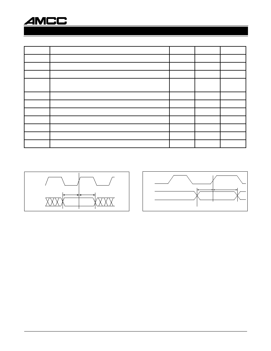
20
S3067
MULTIRATE (OC-48/24/12/3/GBE) SONET/SDH/ATM TRANSCEIVER WITH FEC
October 26, 2000/ Revision A
Figure 9. Transmitter Input Timing
1
Figure 10. Transmitter Output Timing
1
tS
PIN
tH
PIN
PICLKP
PIN[15:0]
TSCLKP
TSD
tSTSD
tHTSD
Table 20. Transmitter AC Timing Characteristics
r
e
t
e
m
a
r
a
P
n
o
i
t
p
i
r
c
s
e
D
n
i
M
x
a
M
s
t
i
n
U
y
c
n
e
u
q
e
r
F
K
L
C
S
T
7
.
2
z
H
G
y
c
n
e
u
q
e
r
F
k
c
o
l
C
S
S
A
P
Y
B
7
.
2
z
H
G
e
l
c
y
C
y
t
u
D
K
L
C
S
T
3
4
7
5
%
r
o
K
L
C
S
R
.
t
.
r
.
w
n
o
i
t
r
o
t
s
i
D
e
l
c
y
C
y
t
u
D
K
L
C
S
T
)
s
e
d
o
m
S
S
A
P
Y
B
r
o
B
E
L
L
,
E
M
I
T
P
L
S
n
I
(
K
L
C
S
S
A
P
Y
B
0
.
5
%
e
l
c
y
C
y
t
u
D
K
L
C
I
P
5
3
5
6
%
S
t
N
I
P
)
9
e
r
u
g
i
F
e
e
S
(
K
L
C
I
P
.
t
.
r
.
w
e
m
i
T
p
u
-
t
e
S
]
0
:
5
1
[
N
I
P
5
.
1
s
n
H
t
N
I
P
)
9
e
r
u
g
i
F
e
e
S
(
K
L
C
I
P
.
t
.
r
.
w
e
m
i
T
d
l
o
H
]
0
:
5
1
[
N
I
P
5
.
0
s
n
P
t
K
L
C
d
e
r
e
t
n
e
c
s
i
O
F
I
F
e
h
t
r
e
t
f
a
t
f
i
r
d
K
L
C
I
P
o
t
K
L
C
P
2
.
5
s
n
S
t
D
S
T
)
9
e
r
u
g
i
F
e
e
S
(
g
n
i
s
i
R
K
L
C
S
T
.
t
.
r
.
w
e
m
i
T
p
u
-
t
e
S
D
S
T
0
0
1
s
p
H
t
D
S
T
)
9
e
r
u
g
i
F
e
e
S
(
g
n
i
s
i
R
K
L
C
S
T
.
t
.
r
.
w
e
m
i
T
d
l
o
H
D
S
T
0
0
1
s
p
e
l
c
y
C
y
t
u
D
N
/
P
K
L
C
P
5
4
5
5
%
Notes on High-Speed Timing:
1. Timing is measured from the cross-over point of the reference signal to the 50% level of the input/output.

21
S3067
MULTIRATE (OC-48/24/12/3/GBE) SONET/SDH/ATM TRANSCEIVER WITH FEC
October 26, 2000 / Revision A
Table 21. AC Receiver Timing Characteristics
l
o
b
m
y
S
n
o
i
t
p
i
r
c
s
e
D
n
i
M
x
a
M
s
t
i
n
U
e
l
c
y
C
y
t
u
D
K
L
C
O
P
5
4
5
5
%
P
t
T
U
O
P
y
a
l
e
D
.
p
o
r
P
d
il
a
V
]
0
:
5
1
[
T
U
O
P
o
t
w
o
L
K
L
C
O
P
)
2
1
e
r
u
g
i
F
e
e
S
(
8
.
1
-
8
.
1
+
s
n
S
t
T
U
O
P
)
z
H
G
8
8
4
.
2
(
K
L
C
O
P
.
t
.
r
.
w
e
m
i
T
p
U
-
t
e
S
]
0
:
5
1
[
T
U
O
P
)
1
1
e
r
u
g
i
F
e
e
S
(
5
2
.
2
s
n
S
t
T
U
O
P
)
z
H
G
7
6
.
2
(
K
L
C
O
P
.
t
.
r
.
w
e
m
i
T
p
u
-
t
e
S
]
0
:
5
1
[
T
U
O
P
)
1
1
e
r
u
g
i
F
e
e
S
(
2
s
n
H
t
T
U
O
P
)
1
1
e
r
u
g
i
F
e
e
S
(
K
L
C
O
P
.
t
.
r
.
w
e
m
i
T
d
l
o
H
]
0
:
5
1
[
T
U
O
P
2
s
n
S
t
D
S
R
)
1
1
e
r
u
g
i
F
e
e
S
(
K
L
C
S
R
.
t
.
r
.
w
e
m
i
T
p
u
-
t
e
S
D
S
R
5
7
s
p
H
t
D
S
R
)
1
1
e
r
u
g
i
F
e
e
S
(
K
L
C
S
R
.
t
.
r
.
w
e
m
i
T
d
l
o
H
D
S
R
5
7
s
p
e
l
c
y
C
y
t
u
D
K
L
C
S
R
0
4
0
6
%
y
c
n
e
u
q
e
r
F
K
L
C
S
R
7
.
2
z
H
G
Figure 12. Receiver Output Timing Diagram
1
Figure 11. Receiver Input Timing Diagram
1
Notes on High-Speed LVPECL Input Timing:
1. Timing is measured from the cross-over point of the reference signal to the 50% level of the output.
tS
RSD
tH
RSD
RSD
RSCLKP
tS
POUT
tP
POUT
tH
POUT
POCLKP
POUT[15:0]
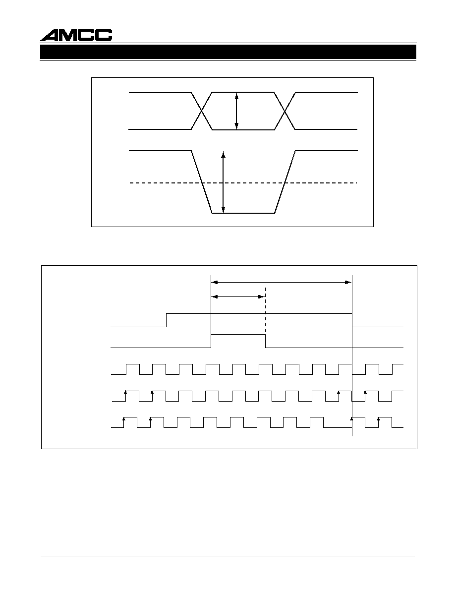
22
S3067
MULTIRATE (OC-48/24/12/3/GBE) SONET/SDH/ATM TRANSCEIVER WITH FEC
October 26, 2000/ Revision A
Figure 13. Differential Voltage Measurement
Note: V(+) ≠ V(-) is the algebraic difference of the input signals.
Figure 14. Phase Adjust Timing
1
V(+)
V(≠)
V(+) ≠ V(-)
0.0V
VSWING
VD = 2 X VSWING
PHERR
TRANSFER CLK
(Internal)
PICLKP
PCLKP
PHINIT
2 BYTE CLOCKS
4-10 BYTE CLOCKS
1. Byte Clock = 155.52 MHz
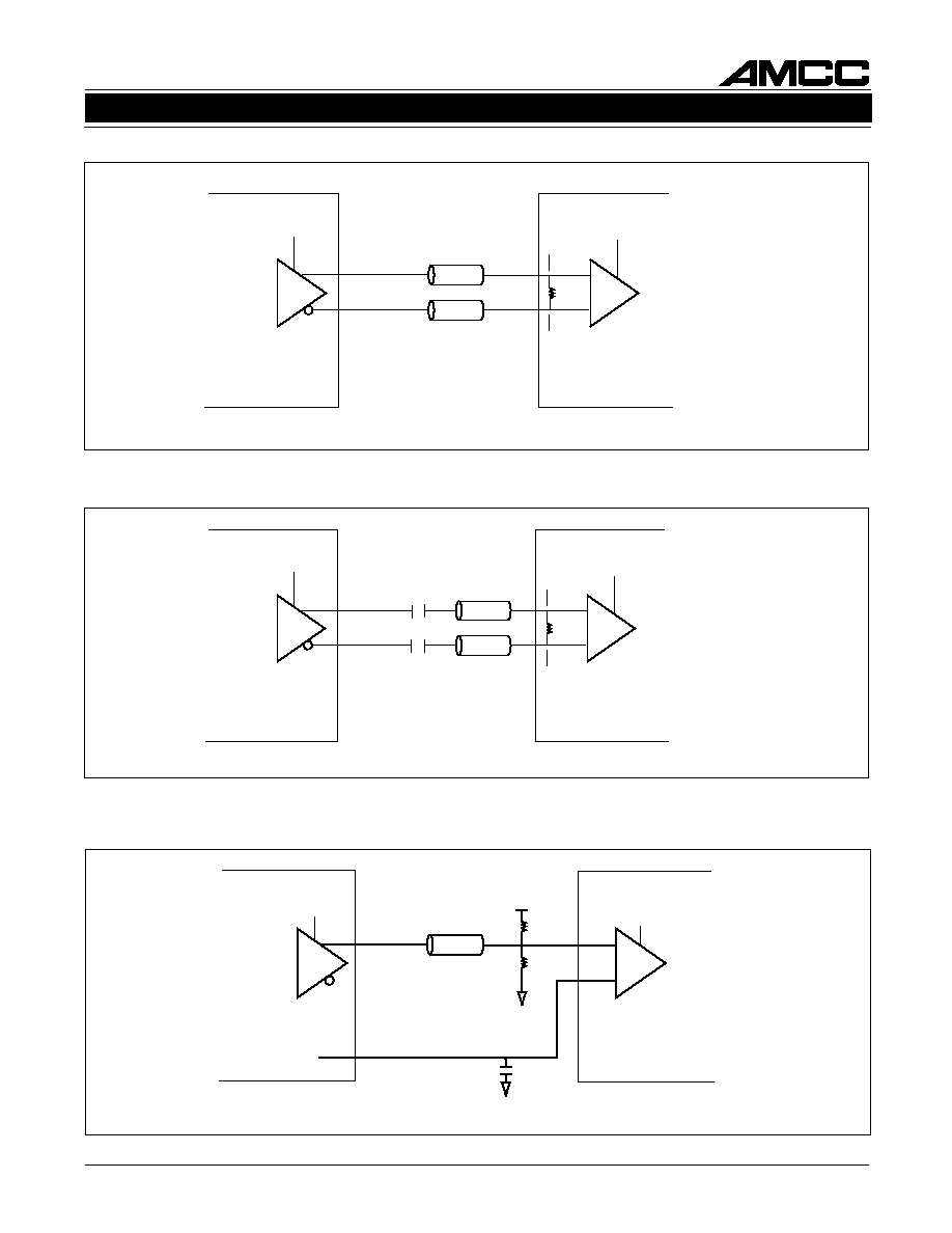
23
S3067
MULTIRATE (OC-48/24/12/3/GBE) SONET/SDH/ATM TRANSCEIVER WITH FEC
October 26, 2000 / Revision A
Figure 16. +5V Differential CML Driver to S3067 Differential CML Input AC Coupled Termination
Figure 15. S3076 to S3067 Differential CML Input Termination
+5 V
SERDATOP/N
SERCLKOP/N
+3.3 V
S3067
RSDP/N
RSCLKP/N
0.01
µ
F
Vcc -0.5 V
0.01
µ
F
100
Vcc -0.5 V
Zo=50
Zo=50
+3.3 V
S3076
SERDATOP/N
SERCLKOP/N
+3.3 V
S3067
RSDP/N
RSCLKP/N
Vcc -0.5 V
100
Vcc -0.5 V
Zo=50
Zo=50
Figure 17. Single-Ended LVPECL Driver to S3067 Single Ended LVPECL Input Termination
+3.3 V
+3.3 V
82
130
S3067
PIN[15:0]
PHINIT
+3.3 V
IVREF
Zo=50
OVREF
0.01
µ
F

24
S3067
MULTIRATE (OC-48/24/12/3/GBE) SONET/SDH/ATM TRANSCEIVER WITH FEC
October 26, 2000/ Revision A
Figure 20. S3067 Single-Ended LVPECL Driver to Single-Ended LVPECL Input Termination
+3.3 V
+3.3 V
51
S3067
Vcc-2 V
Zo=50
0.01
µ
F
POUT[15:0]
PHERR
OVREF
Figure 18. S3067 Differential CML Output to +5V PECL Input AC Coupled Termination
Figure 19. S3067 Single-Ended LVPECL Driver to Single-Ended LVPECL Input Termination
+3.3 V
+5 V
100
S3067
TSDP/N
TSCLKP/N
0.01
µ
F
0.01
µ
F
Zo=50
Zo=50
+3.3 V
+3.3 V
82
130
S3067
Zo=50
3.3 V
POUT[15:0]
PHERR
OVREF
0.01
µ
F

25
S3067
MULTIRATE (OC-48/24/12/3/GBE) SONET/SDH/ATM TRANSCEIVER WITH FEC
October 26, 2000 / Revision A
Figure 21. S3067 Single-Ended LVPECL Driver to Differential LVPECL Input Termination
+3.3 V
+3.3 V
100
100
S3067
POUT[15:0]
PHERR
Zo=50
200
0.1
µ
F
AMAZON
Figure 22. S3067 Differential LVPECL Driver to Differential LVPECL Input Termination
Figure 23. S3067 Differential LVPECL Driver to Differential LVPECL Input Termination
51
S3067
PCLKP/N
POCLKP/N
Zo=50
Zo=50
Vcc≠2
51
Vcc≠2
+3.3 V
+3.3 V
82
130
S3067
PCLKP/N
POCLKP/N
Zo=50
Zo=50
82
130
+3.3 V
+3.3 V
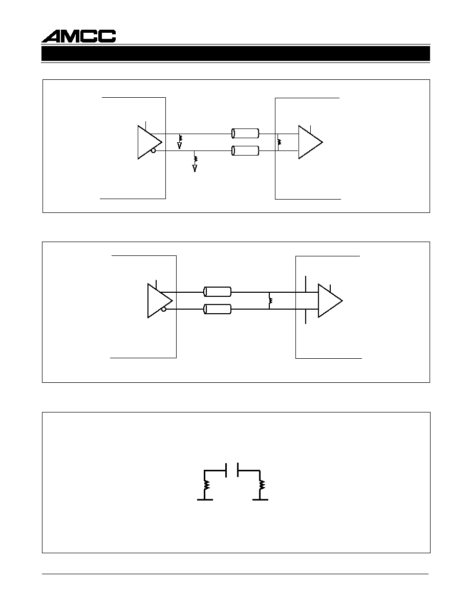
26
S3067
MULTIRATE (OC-48/24/12/3/GBE) SONET/SDH/ATM TRANSCEIVER WITH FEC
October 26, 2000/ Revision A
1 k
10
µ
F
1 k
CAP1
CAP2
Figure 26. External Loop Filter Components
Figure 24. Differential LVPECL Driver to Differential LVPECL Input Termination
1
1. With 100
line-to-line, V
OL
Max increases by 100 mV .
200
S3067
PCLKP/N
POCLKP/N
Zo=50
Zo=50
200
100
+3.3 V
+3.3 V
Figure 25. Differential LVPECL Driver to S3067 Internally Biased Differential LVPECL Inputs
S3067
PICLKP/N
REFCLKP/N
100
+3.3 V
+3.3 V
Zo=50
Zo=50
VCC -0.5 V
VCC -0.5 V

27
S3067
MULTIRATE (OC-48/24/12/3/GBE) SONET/SDH/ATM TRANSCEIVER WITH FEC
October 26, 2000 / Revision A
Ordering Information
AMCC is a registered trademark of Applied Micro Circuits Corporation.
Copyright Æ 2000 Applied Micro Circuits Corporation
D159/R250
AMCC reserves the right to make changes to its products or to discontinue any semiconductor product or service without notice, and
advises its customers to obtain the latest version of relevant information to verify, before placing orders, that the information being relied
on is current.
AMCC does not assume any liability arising out of the application or use of any product or circuit described herein, neither does it
convey any license under its patent rights nor the rights of others.
AMCC reserves the right to ship devices of higher grade in place of those of lower grade.
AMCC SEMICONDUCTOR PRODUCTS ARE NOT DESIGNED, INTENDED, AUTHORIZED, OR WARRANTED TO BE SUITABLE FOR
USE IN LIFE-SUPPORT APPLICATIONS, DEVICES OR SYSTEMS OR OTHER CRITICAL APPLICATIONS.
Applied Micro Circuits Corporation ∑ 6290 Sequence Dr., San Diego, CA 92121
Phone: (858) 450-9333 ∑ (800) 755-2622 ∑ Fax: (858) 450-9885
http://www.amcc.com
C
E
R T I F I E
D
IS
O 9001
X
I
F
E
R
P
E
C
I
V
E
D
E
G
A
K
C
A
P
t
i
u
c
r
i
C
d
e
t
a
r
g
e
t
n
I
≠
S
7
6
0
3
A
G
B
T
6
5
1
≠
B
T
X
XXXX
XX
Prefix Part No. Package