 | –≠–ª–µ–∫—Ç—Ä–æ–Ω–Ω—ã–π –∫–æ–º–ø–æ–Ω–µ–Ω—Ç: S3091 | –°–∫–∞—á–∞—Ç—å:  PDF PDF  ZIP ZIP |
Part Number S3091
Revision A ≠ February 22, 2002
1
DEVICE SPECIFICATION
S3091
SONET/SDH/ATM OC-192 16:1 Transmitter
FEATURES
∑
Silicon Germanium BiCMOS technology
∑
Complies with Telcordia, ITU-T, and G.709
specifications
∑
On-chip high-frequency PLL for clock generation
∑
OC-192 with FEC and Digital Wrapper (DW)
(9.953 to 10.709 Gbps)
∑
Reference frequency of 155.52 or 622.08 MHz
(or equivalent FEC or DW rate)
∑
16-bit parallel, 622.08 Mbps LVDS data path
∑
Lock detect/Phase error indicator
∑
Low jitter CML differential or single-ended
serial interface
∑
Dual +3.3 V and -5.2 V power supply
∑
Supports line timing
∑
Internal FIFO to decouple transmit clocks
∑
311.04 MHz or 622.08 MHz parallel input clock
∑
Programmable skew on 311.04 MHz parallel
clock mode
∑
148-pin CBGA package
∑
Typical power dissipation 2.3 W
APPLICATIONS
∑
SONET/SDH-based transmission systems
∑
SONET/SDH modules
∑
SONET/SDH test equipment
∑
ATM over SONET/SDH
∑
Section repeaters
∑
Add Drop Multiplexers (ADM)
∑
Broad-band cross-connects
∑
Fiber optic terminators
∑
Fiber optic test equipment
GENERAL DESCRIPTION
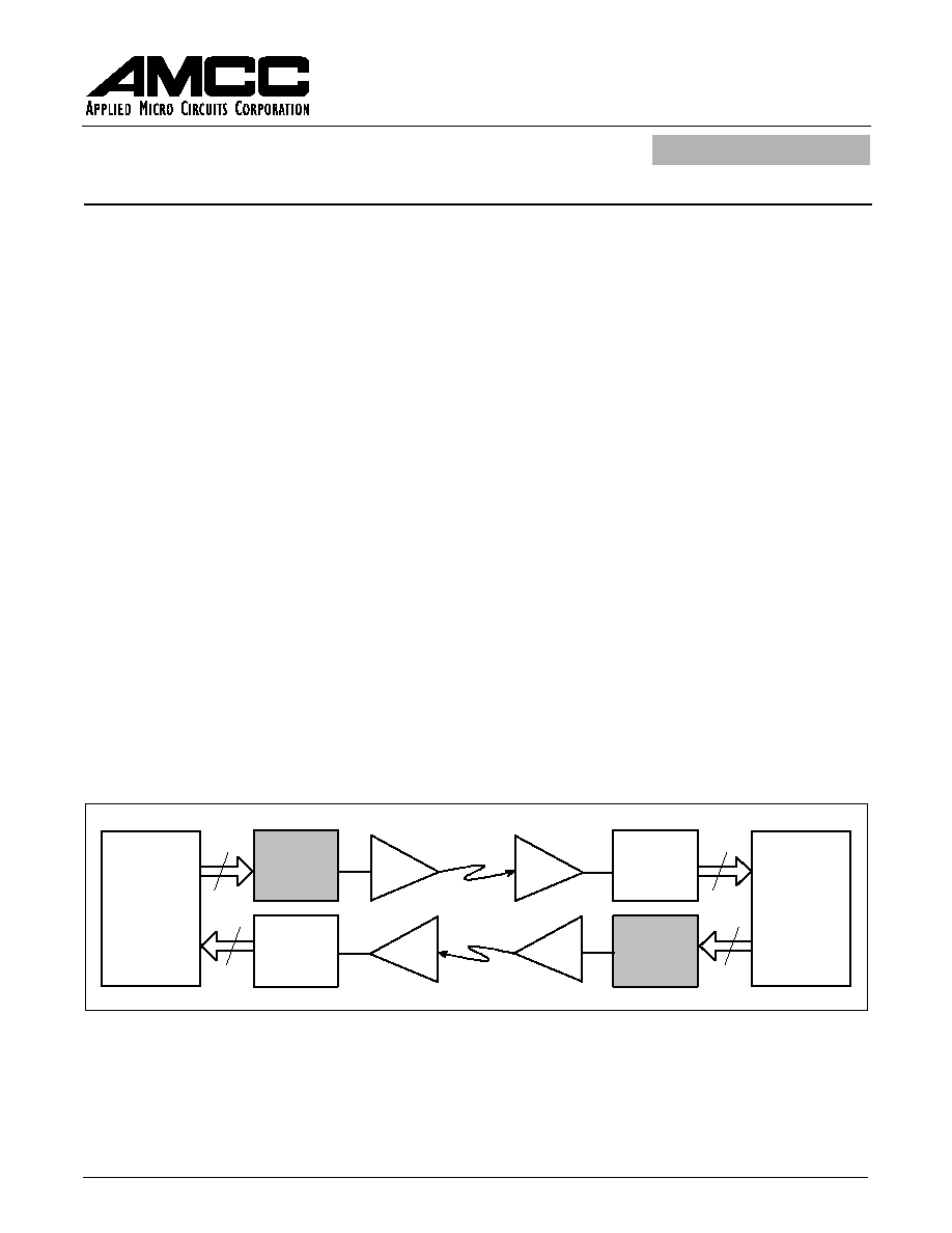
The S3091 SONET/SDH MUX chip is a fully inte-
grated serializer with SONET OC-192 with FEC and
Digital Wrapper (9.953 to 10.709 Gbps) rate capabil-
ity. The chip performs all necessary parallel-to-serial
functions in conformance with SONET/SDH/Digital
Wrapper transmission standards. The device is suit-
able for SONET-based ATM applications. Figure 1
shows a typical network application.
On-chip clock synthesis PLL components are con-
tained in the S3091 MUX chip, allowing the use of a
slower external transmit clock reference. The chip can
be used with a 155.52 or 622.08 MHz reference clock
(or equivalent FEC or DW rate), in support of existing
system clocking schemes.
Figure 1. System Block Diagram
INDUS
(19201),
GANGES
(19202)
or
HUDSON
(19203)
S3091
S3092
S3092
S3091
OTX
ORX
OTX
ORX
16
16
16
16
INDUS
(19201),
GANGES
(19202)
or
HUDSON
(19203)

2
S3091 ≠ SONET/SDH/ATM OC-192 16:1
Transmitter
Revision A ≠ February 22, 2002
DEVICE SPECIFICATION
Contents
FEATURES .............................................................................................................................................................. 1
APPLICATIONS ...................................................................................................................................................... 1
GENERAL DESCRIPTION ...................................................................................................................................... 1
CONTENTS ............................................................................................................................................................. 2
LIST OF FIGURES .................................................................................................................................................. 3
LIST OF TABLES .................................................................................................................................................... 3
SONET OVERVIEW ................................................................................................................................................ 4
Data Rates and Signal Hierarchy ...................................................................................................................... 4
Frame and Byte Boundary Detection ................................................................................................................ 4
S3091 OVERVIEW .................................................................................................................................................. 6
S3091 ARCHITECTURE/FUNCTIONAL DESIGN .................................................................................................. 7
MUX OPERATION ............................................................................................................................................ 7
Clock Divider and Phase Detector ..................................................................................................................... 7
Timing Generator ............................................................................................................................................... 7
Parallel-to-Serial Converter ............................................................................................................................... 8
FIFO .................................................................................................................................................................. 8
FIFO Initialization ............................................................................................................................................... 8
Power Sequencing ............................................................................................................................................ 8
ORDERING INFORMATION ................................................................................................................................. 25

3
S3091 ≠ SONET/SDH/ATM OC-192 16:1
Transmitter
Revision A ≠ February 22, 2002
DEVICE SPECIFICATION
List of Figures
Figure 1. System Block Diagram ............................................................................................................................. 1
Figure 2. SONET Structure ...................................................................................................................................... 4
Figure 3. STS-192 Frame Format ............................................................................................................................ 5
Figure 4. Functional Block Diagram ......................................................................................................................... 6
Figure 5. S3091 Pinout .......................................................................................................................................... 12
Figure 6. S3091 148-Pin CBGA Package .............................................................................................................. 13
Figure 7. AC Input Timing (PICLKP/N = 622.08 MHz) ........................................................................................... 18
Figure 8. AC Input Timing (PICLKP/N = 311.04 MHz) ........................................................................................... 19
Figure 9. Phase Adjust Timing ............................................................................................................................... 20
Figure 10. Differential Voltage Measurement ........................................................................................................ 20
Figure 11. CML Output to -5.2 V ECL Input DC Coupled Termination, Reference Only ....................................... 21
Figure 12. S3091 LVDS Driver to LVDS Input, Reference Only ............................................................................ 21
Figure 13. LVDS Driver to S3091 LVDS Input Direct Coupled Termination, Reference Only ............................... 21
Figure 14. LVDS Driver to S3091 LVDS Input AC Coupled Termination, Reference Only .................................... 22
Figure 15. External Loop Filter ............................................................................................................................... 22
Figure 16. S3091 622.08 MHz REFCLK Phase Noise Limit .................................................................................. 23
Figure 17. S3091 155.52 MHz REFCLK Phase Noise Limit .................................................................................. 24
List of Tables
Table 1. SONET Signal Hierarchy ........................................................................................................................... 4
Table 2. FEC Modes ................................................................................................................................................ 7
Table 3. Reference Frequency ................................................................................................................................ 8
Table 4. Clock Select ............................................................................................................................................... 8
Table 5. Skew Select ............................................................................................................................................... 8
Table 6. Input Pin Assignment and Descriptions ..................................................................................................... 9
Table 7. Output Pin Assignment and Descriptions ................................................................................................ 10
Table 8. Common Pin Assignment and Descriptions ............................................................................................. 11
Table 9. Thermal Management .............................................................................................................................. 13
Table 10. Performance Specifications ................................................................................................................... 14
Table 11. Absolute Maximum Ratings ................................................................................................................... 15
Table 12. Recommended Operating Conditions .................................................................................................... 15
Table 13. LVTTL Input DC Characteristics ............................................................................................................ 16
Table 14. LVTTL Output DC Characteristics ......................................................................................................... 16
Table 15. Differential CML Output DC Characteristics ........................................................................................... 16
Table 16. Internally Biased Differential ECL Input DC Characteristics .................................................................. 16
Table 17. Internally Biased LVDS Input Characteristics ........................................................................................ 17
Table 18. LVDS Output DC Characteristics (See Figure 12) ................................................................................. 17
Table 19. AC Transmitter Timing Characteristics (PICLKP/N = 622.08 MHz) ....................................................... 18
Table 20. AC Transmitter Timing Characteristics (PICLKP/N = 311.04 MHz) ....................................................... 19
Table 21. External Loop Filter Components .......................................................................................................... 19
4
S3091 ≠ SONET/SDH/ATM OC-192 16:1
Transmitter
Revision A ≠ February 22, 2002
DEVICE SPECIFICATION
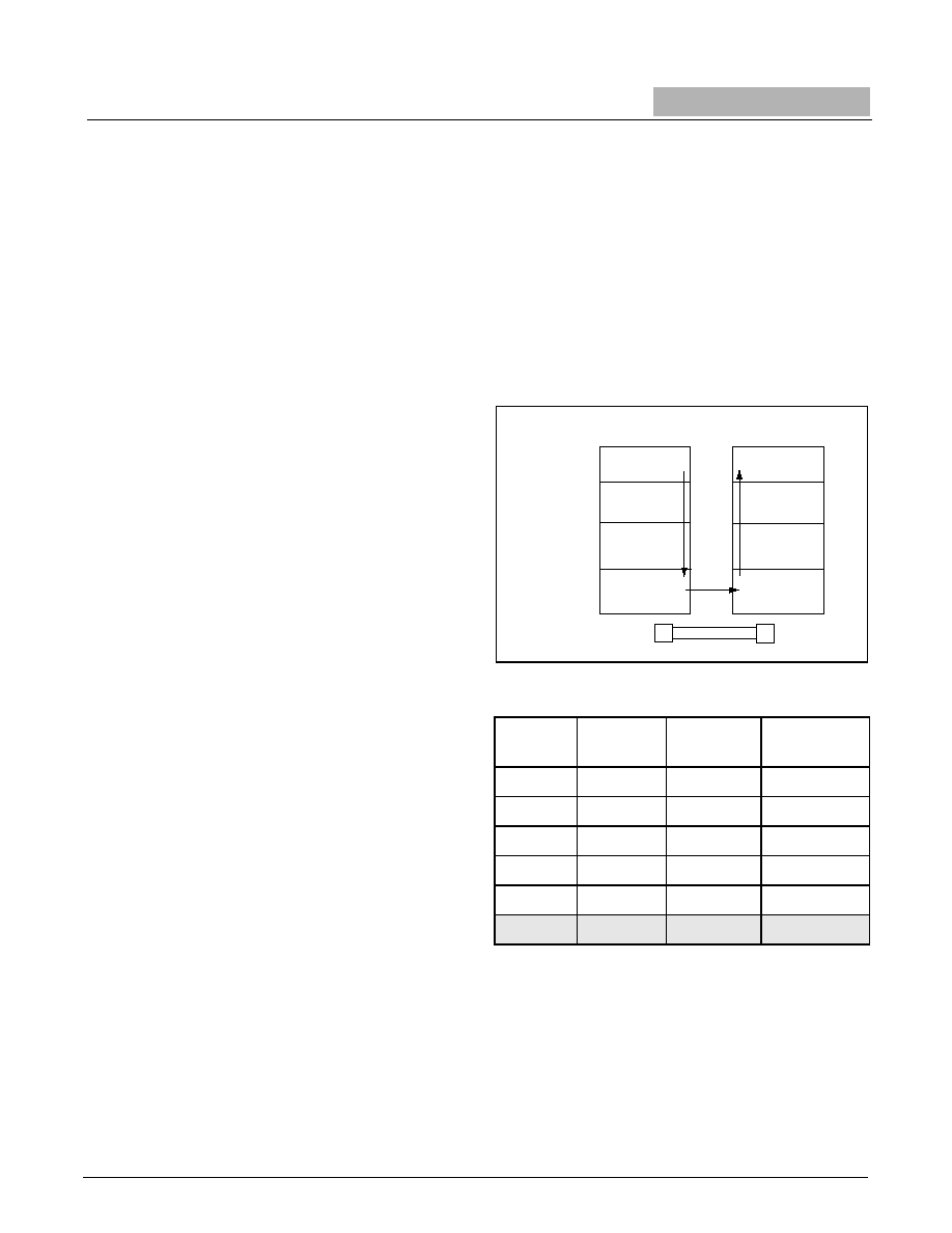
SONET OVERVIEW
Synchronous Optical Network (SONET) is a standard
for connecting one fiber system to another at the opti-
cal level. SONET, together with the Synchronous
Digital Hierarchy (SDH) administered by the ITU-T,
forms a single international standard for fiber intercon-
n e c t b e tw e e n te l e p h o n e n e t w o r k s o f d iff e re n t
countries. SONET is capable of accommodating a
variety of transmission rates and applications.
The SONET standard is a layered protocol with four
separate layers defined. These are:
∑ Photonic
∑ Section
∑ Line
∑ Path
Figure 2 shows the layers and their functions. Each of
the layers has overhead bandwidth dedicated to
administration and maintenance. The photonic layer
simply handles the conversion from electrical to optical
and back with no overhead. It is responsible for trans-
mitting the electrical signals in optical form over the
physical media. The section layer handles the trans-
port of the framed electrical signals across the optical
cable from one end to the next. Key functions of this
layer are framing, scrambling, and error monitoring.
The line layer is responsible for the reliable transmis-
sion of the path layer information stream carrying
voice, data, and video signals. Its main functions are
synchronization, multiplexing, and reliable transport.
The path layer is responsible for the actual transport of
services at the appropriate signaling rates.
Data Rates and Signal Hierarchy
Table 1 contains the data rates and signal designa-
tions of the SONET hierarchy. The lowest level is
the basic SONET signal, referred to as the synchro-
nous transport signal level-1 (STS-1). An STS-N
signal is made up of N byte-interleaved STS-1 sig-
nals. The optical counterpart of each STS-N signal
is an optical carrier level-N signal (OC-N). The chip
supports OC-192 with FEC and Digital Wrapper
(9.95328 to 10.709 Gbps) rates.
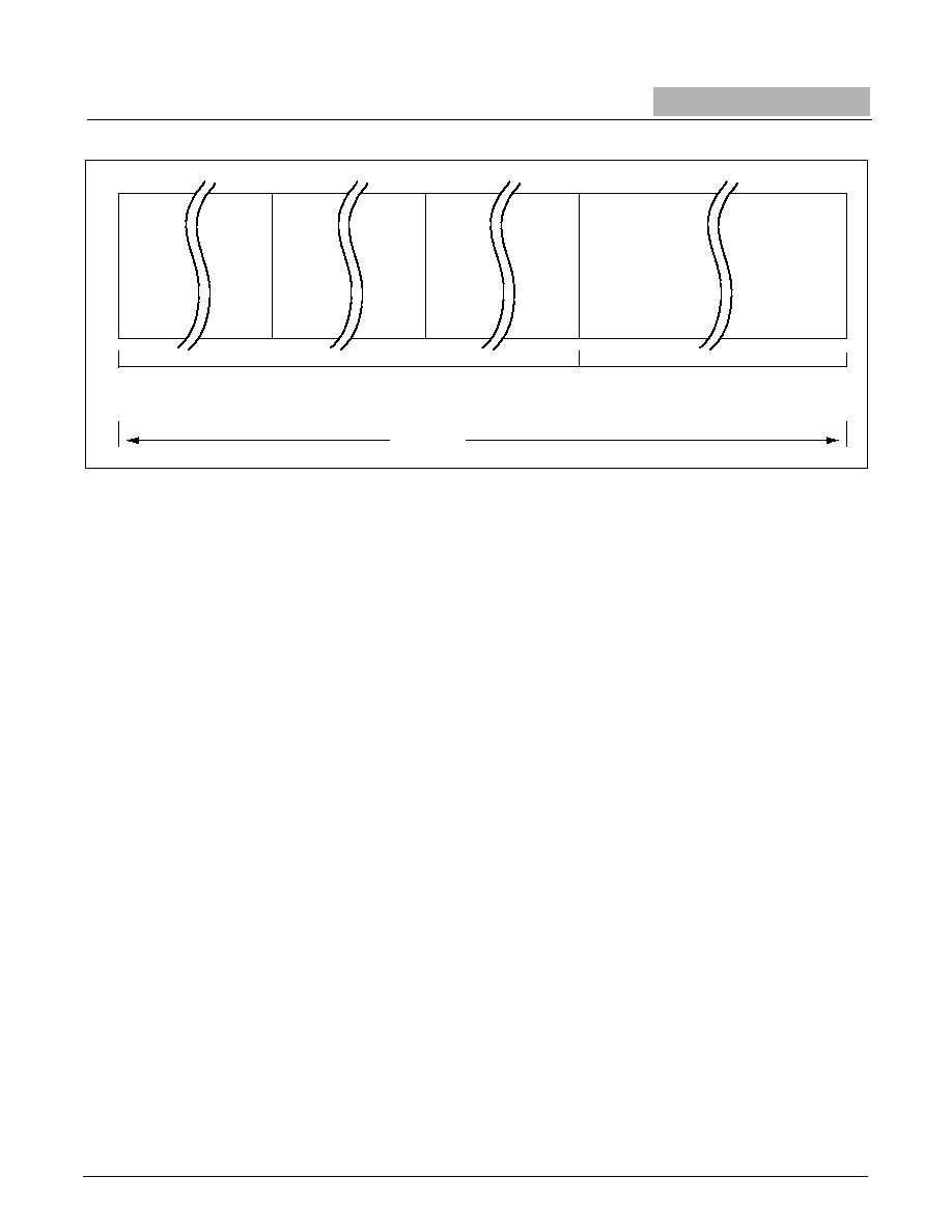
Frame and Byte Boundary Detection
The SONET/SDH fundamental frame format for
STS-192 consists of 576 transport overhead bytes
followed by Synchronous Payload Envelope (SPE)
bytes. This pattern of 576 overhead and 16,704
SPE bytes is repeated nine times in each frame.
Frame and byte boundaries are detected using the
A1 and A2 bytes found in the transport overhead.
(See Figure 3.)
For more details on SONET operations, refer to the
Bellcore SONET standard document.
Figure 2. SONET Structure
Table 1. SONET Signal Hierarchy
Elec.
ITU-T
Optical
Data Rate
(Mbps)
STS-1
OC-1
51.84
STS-3
STM-1
OC-3
155.52
STS-12
STM-4
OC-12
622.08
STS-24
STM-8
OC-24
1244.16
STS-48
STM-16
OC-48
2488.32
STS-192
STM-64
OC-192
9953.28
End Equipment
Payload to
SPE mapping
Maintenance,
protection,
switching
Optical
transmission
Scrambling,
framing
Fiber Cable
End Equipment
Functions
Path layer
Line layer
Section layer
Photonic layer
Photonic layer
Section layer
Line layer
Path layer
5
S3091 ≠ SONET/SDH/ATM OC-192 16:1
Transmitter
Revision A ≠ February 22, 2002
DEVICE SPECIFICATION
Figure 3. STS-192 Frame Format
9
Ro
ws
192 A1
Bytes
192 A2
Bytes
A1 A1
A1 A1
A2 A2
A2 A2
Transport Overhead
576 Columns
576 x 9 = 5,184 bytes
Synchronous Payload Envelope
16,704 Columns
16,704 x 9 = 150,336 bytes
125
µsec