 | –≠–ª–µ–∫—Ç—Ä–æ–Ω–Ω—ã–π –∫–æ–º–ø–æ–Ω–µ–Ω—Ç: S4403-66 | –°–∫–∞—á–∞—Ç—å:  PDF PDF  ZIP ZIP |

Applied Micro Circuits Corporation
6195 Lusk Blvd., San Diego, CA 92121 ∑ (619) 450-9333
Page 1
DEVICE SPECIFICATION
BiCMOS PECL CLOCK GENERATOR
S4405
Æ
FEATURES
∑ Generates six clock outputs from 20 MHz to 80
MHz (HFOUT operates from 10 MHz to 40 MHz)
∑ Allows PECL or TTL reference input
∑ Provides differential PECL output at up to 160
MHz
∑ 21 selectable phase/frequency relationships for
the clock outputs
∑ Compensates for clock skew by allowing output
delay adjustment down to 3.125 ns increments
∑ TTL outputs have less than 400 ps maximum
skew
∑ Lock Detect output indicates loop status
∑ Internal PLL with VCO operating at 160 to 320
MHz
∑ Test Enable input allows VCO bypass for open-
loop operation
∑ Maximum 1.0 ns of phase error (750 ps from
part to part)
∑ Proven 1.0 micron BiCMOS technology
∑ Single +5V power supply operation
∑ 44 PLCC package
APPLICATIONS
∑ CMOS ASIC Systems
∑ High-speed Microprocessor Systems
∑ Backplane Clock Deskew and Distribution
GENERAL DESCRIPTION
The S4405 BiCMOS clock generators allow the user
to generate multiphase TTL clocks in the 10≠80 MHz
range with less than 400 ps of skew. Use of a simple
off-chip filter allows an entire 160≠320 MHz phase-
locked loop (PLL) to be implemented on-chip. Divide-
by-two and times-two outputs allow the ability to
generate output clocks at half, equal to, or twice the
reference clock input frequency. The reference is se-
lectable to be either TTL or PECL. By using the pro-
grammable divider and phase selector, the user can
select from up to 21 different output relationships.
The outputs can be phase-adjusted in increments as
small as 3.125 ns to tailor the clocks to exact system
requirements.
Implemented in AMCC's proven 1.0 micron BiCMOS
technology, the S4405 generates six TTL outputs
and one differential PECL output. Output enables are
provided for the various TTL banks, allowing clock
control for board and system tests.
Figure 1. Clock Generator Block Diagram
PHASE
DETECTOR
CHARGE
PUMP
VCO
I
0
I
1
MUX
SELECT
TTLREF
REFCLK
FBCLK
TSTEN
DIVSEL
PHSEL0
PHSEL1
RESET
OUTEN0
OUTEN1
DIVIDER
AND
PHASE
CONTROL
LOGIC
HFOUT
X2FOUT
FOUT0
FOUT1
FOUT2
FOUT3
LOCK
FILTER
Digital
+5V
0V
14K
Analog
+5V
0V
˜ 2
PECLP
MUX
PECLREFN
INPSEL
PECLN
I
0
I
1
S
PECLREFP

Applied Micro Circuits Corporation
6195 Lusk Blvd., San Diego, CA 92121 ∑ (619) 450-9333
Page 2
S4405
FUNCTIONAL DESCRIPTION
FUNCTIONAL DESCRIPTION
This BiCMOS clock generator is designed to allow
the user to generate TTL clocks, in the 10≠80 MHz
range, with less than 400 ps of skew. Implemented
in AMCC's 1.0
µ
BiCMOS technology, the internal
VCO, phase detector, and programmable divider and
phase selector allow the user to tailor the TTL output
clocks for his/her system needs. The internal VCO
can operate between 160 to 320 MHz, and the pro-
grammability allows the user to generate TTL output
clocks in the 10≠80 MHz range, and a differential
+5V referenced ECL output at 80≠160 MHz.
The clock generator offers the user the ability to se-
lect the appropriate phase relationship among the
four FOUT0≠3 TTL clock outputs. The phase selec-
tion choices are shown in Table 2.
The clock generator also allows the user to choose
the divide-by ratio between the VCO frequency and
the frequency of the FOUT0≠3 signals. The VCO fre-
quency can be divided by 4 when DIVSEL is low, and
divided by 8 when DIVSEL is high. The divide ratio
between the VCO and the pseudo ECL outputs,
PECLP and PECLN, is a fixed divide-by-2.
The clock generator also has two output enable in-
puts which can be used to control which outputs
toggle. OUTEN0 controls the HFOUT and X2FOUT
outputs, and OUTEN1 controls the FOUT0≠3 out-
puts. When the output enables are high, the outputs
are disabled, and held in a high state.
REFCLK can be driven by either the TTLREF or
PECLREF inputs. The reference clock source is se-
lected with the INPSEL input. When INPSEL is low,
the TTLREF input is selected as the reference clock.
The FOUT0≠3 outputs are the main TTL output
clocks that the generator supplies. The frequency of
these outputs is determined by the REFCLK clock
frequency and the output clock that is tied to the
FBCLK input. FOUT0≠3 will be equal to REFCLK,
half of REFCLK, or twice the frequency of REFCLK.
The X2FOUT TTL output provides a clock signal that
is identical to the FOUT0 output in the divide-by-4
mode, but twice the FOUT0 frequency (max. freq. of
66 MHz) in the divide-by-8 mode. The HFOUT TTL
output provides a clock signal that is also in phase with
the FOUT0 output, but at half the FOUT0 frequency.
FILTER is the analog signal from the phase detector
going into the VCO. This pin is provided so a simple
external filter (a single resistor and one capacitor)
can be included in the phase-locked loop of the clock
generator.
The LOCK output goes high when the reference
clock and FBCLK are within 2≠4 ns of each other.
This output tells the user that the PLL is in lock.
Three pins are included for test purposes. TESTEN
allows the chip to use the REFCLK signal instead of
the VCO output to clock the chip. This is used during
chip test to allow the counters and control logic to be
tested independently of the VCO. The RESET pin
initializes the internal counter flip-flops to zeros, but
several clock cycles are necessary before the out-
puts go to a zero state.
The minimum phase delay between FOUT0≠3 sig-
nals is a function of the VCO frequency. The VCO
frequency can be determined by multiplying the out-
put frequency by the divide-by ratio of four or eight.
The minimum phase delay is equal to the period of
the VCO frequency: M
P
= 1/VCO freq. Since the VCO
can operate in the 160 MHz to 320 MHz range, the
range of minimum phase delay values is 6.25 ns to
3.125 ns. Table 1 shows various FOUT/VCO fre-
quencies and the associated phase resolution.
The charge pump and VCO portion of the chip use a
separate analog power supply. This supply is brought
onto the chip through a distinct set of power and
ground pins. This supply should be free of digital
switching noise.
Example:
In a typical system, designers may need several low-
skew outputs, one early clock, one late clock, a clock
at half the input clock frequency, and one at twice
the input clock frequency. This system requirement
FOUT0≠3
Divider
VCO
Min Phase
Freq
Select
Freq
Resolution
80 MHz
4
320 MHz
3.125 ns
66 MHz
4
266 MHz
3.75 ns
50 MHz
4
200 MHz
5.0 ns
40 MHz
4
160 MHz
6.25 ns
40 MHz
8
320 MHz
3.125 ns
33 MHz
8
266 MHz
3.75 ns
25 MHz
8
200 MHz
5.0 ns
20 MHz
8
160 MHz
6.25 ns
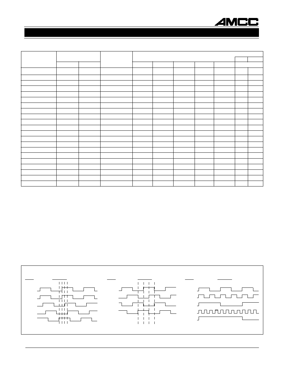
Table 1. Example Phase Resolution
PHSEL1 PHSEL0
Phase Relationship
0
0
All at same phase
0
1
Outputs skewed by 90 degrees from
each other
1
0
FOUT1 leads FOUT0 by minimum
phase, FOUT2 lags FOUT0 by
minimum phase, and FOUT3 lags
FOUT0 by 90 degrees
1
1
Outputs skewed by minimum phase
(determined by the divider selection,
and the VCO frequency) from each
other.
Note:
The PECL output is not affected by the phase select inputs.
Table 2. Phase Selections
Applied Micro Circuits Corporation
6195 Lusk Blvd., San Diego, CA 92121 ∑ (619) 450-9333
Page 3
FUNCTIONAL DESCRIPTION
S4405
can be met by setting PHSEL1 to 1, PHSEL0 to 0,
and feeding back FOUT0 to the FBCLK input (Row
10 of Table 3). The result is that FOUT0 will be
phase-aligned to the reference clock, FOUT1 will
lead the reference clock by a minimum phase delay,
FOUT2 will lag the reference clock by a minimum
phase delay, FOUT3 will phase-lag the reference
clock by 90
∞
, HFOUT will be phase-aligned with the
reference clock but at half the frequency, and
X2FOUT will be either phase-aligned at the same
frequency as the reference clock if DIVSEL = 0, or at
twice the frequency if DIVSEL = 1.
Enabling Outputs
The S4405 has two output-enable inputs that control
which outputs toggle. When held LOW, OUTEN0
controls the frequency doubler output X2FOUT and
the half-frequency output HFOUT. OUTEN1 controls
the FOUT0≠3 outputs. When an output enable pin is
held High, its associated outputs are disabled and
held in a High state.
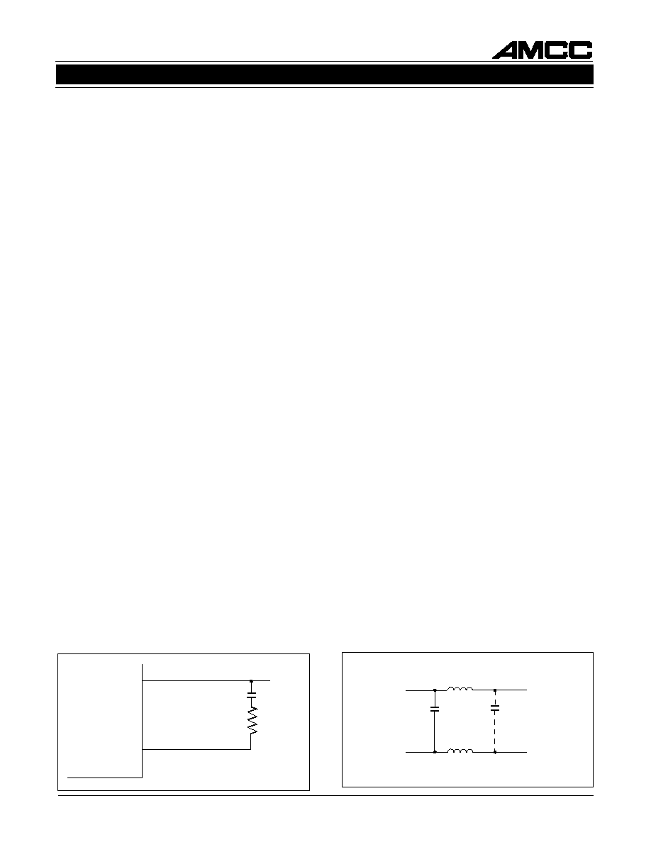
Filter
The FILTER output is a tap between the analog out-
put of the phase detector and the VCO input. This pin
allows a simple external filter (Figure 2) to be in-
cluded in the PLL. AMCC recommends the use of the
filter component values shown. This filter was chosen
for its ability to reduce the output jitter and filter out
noise on the reference clock input.
Reset
When the RESET pin is pulled low, all the internal
states go to zero, but the outputs will not go low until
one clock cycle later (VCO/2 or period of the refer-
ence clock). After the chip is reset, the PLL requires
a resynchronization time before lock is again achieved.
Lock Detect
A lock detect function is provided by the LOCK out-
put. When the selected reference clock and FBCLK
Figure 2. External PLL Filter
Figure 3. External Power Supply Filter
ANALOG +5V
0.1 µF
DIGITAL +5V
DIGITAL GND
ANALOG GND
FB1
FB2
10 µF
Tantalum
(optional)
are within 2≠4 ns of each other, the PLL is in lock,
and the LOCK output goes High.
Power Supply Considerations
Power for the analog portion of the S4405 chips must
be isolated from the digital power supplies to mini-
mize noise on the analog power supply pins. This
isolation between the analog and digital power sup-
plies can be accomplished with a simple external
power supply filter (Figure 3). The analog power
planes are connected to the digital power planes
through single ferrite beads (FB1 and FB2) or induc-
tors capable of handling 25 mA. The recommended
value for the inductors is in the range from 5 to
100
µ
H, and depends upon the frequency spectrum of
the digital power supply noise. The ferrite beads
should exhibit 75
impedance at 10 MHz.
Decoupling capacitors are also very important to
minimize noise. The decoupling capacitors must
have low lead inductance to be effective, so ceramic
chip capacitors are recommended. Decoupling ca-
pacitors should be located as close to the power pins
as physically possible. And the decoupling should be
placed on the top surface of the board between the
part and its connections to the power and ground
planes.
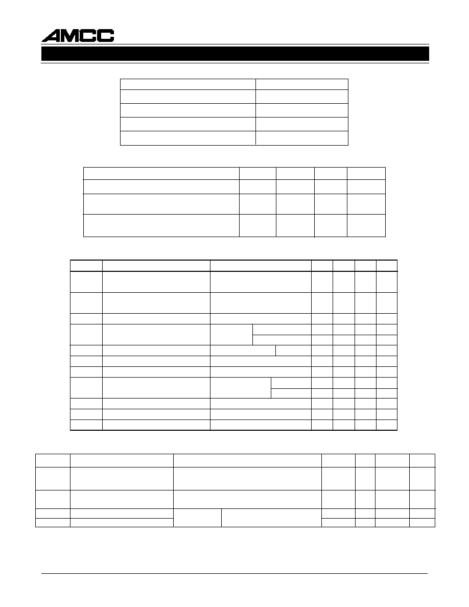
BOARD LAYOUT CONSIDERATIONS
∑ The S4405 is sensitive to noise on the Analog +5 V
and Filter pins. Care should be taken during board
layout for optimum results.
∑ All decoupling capacitors (C1≠C4 = 0.1
µ
F) should
be bypassed between VCC and GND, and placed as
close to the chip as possible (preferably using ce-
ramic chip caps) and placed on top of board between
S4405 and the power and ground plane connections.
∑ No dynamic signal lines should pass through or
beneath the filter circuitry area (enclosed by dashed
lines in Figure 4) to avoid the possibility of noise due
to crosstalk.
A +5V
0.1 µF
1.5k
32
31
S4405
A VCC
FILTER

Applied Micro Circuits Corporation
6195 Lusk Blvd., San Diego, CA 92121 ∑ (619) 450-9333
Page 4
∑ The analog VCC supply can be a filtered digital
VCC supply as shown below. The ferrite beads or
inductors, FB1 and FB2, should be placed within
three inches of the chip.
∑ The analog VCC plane should be separated from the
digital VCC and ground planes by at least 1/8 inch.
S4405
PIN DESCRIPTIONS
PHSEL0. This input, along with PHSEL1, allows se-
lection of the phase relationship among the four
FOUT0≠FOUT3 outputs. See Tables 2 and 3 for the
selection choices.
PHSEL1. Along with PHSEL0, allows selection of the
phase relationship among the four FOUT0≠FOUT3
outputs. See Tables 2 and 3 for the selection
choices.
OUTEN0. Active Low. Output enable signal that con-
trols which outputs toggle. Controls the frequency
doubler output (X2FOUT) and the half-frequency out-
put (HFOUT).
OUTEN1. Active Low. Output enable signal that con-
trols which outputs toggle. Controls the FOUT0≠
FOUT3 outputs.
RESET. Active Low. Initializes internal states for test
purposes.
TSTEN. Active High. Allows REFCLK to drive the
divider phase adjust circuitry, after the first divide-by-
two stage. Therefore, REFCLK can be divided by two
in the divide-by-four mode, and divided by four in the
divide-by-eight mode, and used to directly sequence
the outputs.
INPSEL. Allows user to select between TTLREF and
PECLREF reference frequencies. When INPSEL is
High, the PECLREF input is selected.
Output Signals
FILTER. A tap between the analog output of the
phase detector and the VCO input. Allows a simple
external filter (a single resistor and capacitor) to be
included in the PLL.
X2FOUT. Provides a clock signal identical to the
FOUT0 output in the divide-by-four mode and twice
the FOUT0 frequency (maximum of 80 MHz) in the
divide-by-eight mode.
FOUT0. Clock output.
FOUT1. Clock output.
FOUT2. Clock output.
FOUT3. Clock output.
HFOUT. Provides a clock signal in phase with the
FOUT0 output, but at half the FOUT0 frequency in
both the divide-by-four and divide-by-eight modes.
PECLP/N. Differential PECL output, always one-half
the VCO frequency.
LOCK. Goes high when the reference clock and
FBCLK are within 2≠4 ns of each other, demonstrat-
ing that the PLL is in lock.
Test Capabilities
The TSTEN input allows users to bypass the VCO and
provide their own clock through the selected reference
clock input. When TSTEN is High, the VCO is turned
off and the REFCLK signal drives the divider/phase
adjust circuitry, directly sequencing the outputs. The
TSTEN and REFCLK inputs join the divider circuitry
after the initial divide-by-two stage. Therefore, REFCLK
is divided by two in the divide-by-four mode and di-
vided by four in the divide-by-eight mode.
PIN DESCRIPTIONS
Input Signals
TTLREF. TTL. Frequency reference supplied by the
user that, along with the output tied to the FBCLK
input, determines the frequency of the FOUT0≠
FOUT3 outputs. INPSEL is used to select between
this reference and the PECL reference PECLREFP/N.
PECLREFP/N. Differential PECL. Frequency refer-
ence supplied by the user. Selectable by the INPSEL
input.
FBCLK. Feedback clock that, along with the refer-
ence clock input, determines the frequency of the
FOUT0≠FOUT3 outputs. One output is selected to
feed back to this input. (See Table 3.)
DIVSEL. Controls the divider circuit that follows the
VCO. When DIVSEL is low, the VCO frequency is
divided by four. When DIVSEL is high, the VCO fre-
quency is divided by eight. (See Tables 1 and 3.)
34
33
32
31
1.5K
0.1
µ
F
0.1
µ
F
A +5V
D GND
D +5V
FB2
FB1
S4405
A GND
Figure 4. Board Layout
Applied Micro Circuits Corporation
6195 Lusk Blvd., San Diego, CA 92121 ∑ (619) 450-9333
Page 5
Table 3. Output Select Matrix
Configuration
Select Pins
Output Fed
Output Phase Relationships
Number
to FBCLK
˜
4
˜
8
PHSEL1 PHSEL0
FOUT0
FOUT1
FOUT2
FOUT3
HFOUT
X2FOUT
1
0
0
FOUT0≠FOUT3
0
0
0
0
0/2
0
2(0)
2
0
0
HFOUT
2(0)
2(0)
2(0)
2(0)
0
2(0)
4(0)
3
0
0
X2FOUT (
˜
8)
0/2
0/2
0/2
0/2
0/4
0
4
0
1
FOUT0
0
Q
2Q
3Q
0/2
0
2(0)
5
0
1
FOUT1
≠Q
0
Q
2Q
≠Q/2
≠Q
2(≠Q)
6
0
1
FOUT2
≠2Q
≠Q
0
Q
≠2Q/2
≠2Q
2(≠2Q)
7
0
1
FOUT3
≠3Q
≠2Q
≠Q
0
≠3Q/2
≠3Q
2(≠3Q)
8
0
1
HFOUT
2(0)
2(Q)
2(2Q)
2(3Q)
0
2(0)
4(0)
9
0
1
X2FOUT (
˜
8)
0/2
Q/2
2Q/2
3Q/2
0/4
0
10
1
0
FOUT0
0
≠t
t
Q
0/2
0
2(0)
11
1
0
FOUT1
t
0
2t
Q+t
t/2
t
2(t)
12
1
0
FOUT2
≠t
≠2t
0
Q≠t
≠t/2
≠t
2(≠t)
13
1
0
FOUT3
≠Q
≠Q≠t
≠Q+t
0
≠Q/2
≠Q
2(≠Q)
14
1
0
HFOUT
2(0)
2(≠t)
2(t)
2(Q)
0
2(0)
4(0)
15
1
0
X2FOUT (
˜
8)
0/2
≠t/2
t/2
Q/2
0/4
0
16
1
1
FOUT0
0
t
2t
3t
0/2
0
2(0)
17
1
1
FOUT1
≠t
0
t
2t
≠t/2
≠t
2(≠t)
18
1
1
FOUT2
≠2t
≠t
0
t
≠2t/2
≠2t
2(≠2t)
19
1
1
FOUT3
≠3t
≠2t
≠t
0
≠3t/2
≠3t
2(≠3t)
20
1
1
HFOUT
2(0)
2(t)
2(2t)
2(3t)
0
2(0)
4(0)
21
1
1
X2FOUT (
˜
8)
0/2
t/2
2t/2
3t/2
0/4
0
Notes:
1.
"0" implies the output is aligned with the reference clock.
2.
"t" implies the output lags the reference clock by a minimum phase delay.
3.
"Q" implies the output lags the reference clock by 90
∞
of phase.
4.
"≠t" implies the output leads the reference clock by a minimum phase delay.
5.
"≠Q" implies the output leads the reference clock by 90
∞
of phase.
6.
"2( )" implies the output is at twice the frequency of the reference clock.
7.
"/2" implies the output is at half the frequency of the reference clock.
8.
The PECLN/P Differential PECL output is not affected by the PHSEL inputs.
0
t
≠t
2t
TTLREF
0
Q
2Q
≠Q
TTLREF
2(0)
0/2
0/4
4(0)
TTLREF
0∞ 90∞ 180∞
Table
entry
Table
entry
Table
entry
Waveform
Waveform
Waveform
≠t
t 2t
≠90∞
Legend
OUTPUT SELECT MATRIX
S4405
Applied Micro Circuits Corporation
6195 Lusk Blvd., San Diego, CA 92121 ∑ (619) 450-9333
Page 6
S4405
ELECTRICAL CHARACTERISTICS
ABSOLUTE MAXIMUM RATINGS
TTL Supply Voltage VCC (GND = 0)
7.0 V
TTL Input Voltage (GND = 0)
5.5 V
Operating Temperature
0
∞
C to 70
∞
C ambient
Operating Junction Temperature TJ
+ 130
∞
C
Storage Temperature
≠65
∞
C to +150
∞
C
Symbol
VIH2
Input HIGH Voltage (TTL)
2.0
2.4
2.0
-25
V
Guaranteed input HIGH voltage for
all inputs
VIL2
Input LOW Voltage (TTL)
VIK
Input clamp diode voltage
0.8
V
-1.2
0.5
-0.8
V
V
V
V
10
µA
Guaranteed input LOW voltage for
all inputs
VCC = Min, IIN = -18mA
II
Input HIGH Current at Max
1.0
mA
-300
-50
µA
µA
VCC = Max, VIN = VCC
IOS4
Output short circuit current
-100
mA
VCC = Max, VOUT = 0V
ICC
Static
95
mA
VCC = Max
ICCT
Total ICC (Dynamic and Static)
200
mA
CLOAD = 25pF at 50 MHz
IIH
Input HIGH Current
VCC = Min, VIN = 2.7V
VCC = Min, VIN = 0.5V
VOH
Output HIGH Voltage
VCC = Min
VOL
Output LOW Voltage
VCC = Min
IIL
Input LOW Current
IOH = -12mA3
IOH = -24mA3
IOL = 24mA3
Parameter
Min
Typ
1
Max Units
DC Test Conditions
INPSEL
Others
DC CHARACTERISTICS (TTL I/O)
Parameter
Min
Nom
Max
Units
TTL Supply Voltage (VCC)
4.75
5.0
5.25
V
Operating Temperature
0
--
70
∞
C
(ambient)
(ambient)
Junction Temperature
--
--
130
∞
C
RECOMMENDED OPERATING CONDITIONS
DC CHARACTERISTICS (PECL I/O)
Symbol
Parameter
DC Test Conditions
Min
Typ
1
Max
Units
V
IH
2
Input HIGH Voltage (PECL)
Guaranteed input HIGH voltage
V
CC
≠1145
V
CC
≠600
V
for all inputs
V
IL
2
Input LOW Voltage (PECL)
Guaranteed input LOW voltage
V
CC
≠2000
V
CC
≠1450
V
for all inputs
V
OH
Output HIGH voltage
V
CC
≠1075
V
CC
≠650
V
V
OL
Output LOW voltage
V
CC
≠1980
V
CC
≠1585
V
V
CC
= 5.0 V
Load = 50
to V
CC
≠2V
1. Typical limits are at 25
∞
C, V
CC
= 5.0V.
2. These input levels provide zero noise immunity and should only be tested in a static, noise-free environment.
3. I
OH
/I
OL
values indicated are for DC test correlation. Actual dynamic currents are significantly higher and are optimized to
balance rise and fall times.
4. Maximum test duration one second.
Applied Micro Circuits Corporation
6195 Lusk Blvd., San Diego, CA 92121 ∑ (619) 450-9333
Page 7
AC SPECIFICATIONS
S4405
Table 4. AC Specifications
Symbol
Description
Min
Max
Min
Max
Units
f
VCO
VCO Frequency
160
266
160
320
MHz
f
REF
REFCLK Frequency
10
66
10
80
MHz
MPW
REF
REFCLK Minimum Pulse Width
5.0
5.0
ns
t
PE
Phase Error between TTLREF and FBCLK
-1
0
-1
0
ns
t
PEP
Phase Error between PECLREF and FBCLK
-3
-1
-3
-1
ns
t
PED
Phase Error Difference from Part to Part
1
0
750
0
750
ps
t
SKEW
Output Skew
2
(TTL)
0
400
0
400
ps
t
DC
Output Duty Cycle
45
55
45
55
%
f
PECL
PECLP/N Frequency
80
132
80
160
MHz
f
FOUT
FOUT Frequency
3
(TTL)
20
66
20
80
MHz
f
HFOUT
HFOUT Frequency
3
10
33
10
40
MHz
f
2XFOUT
2XFOUT Frequency
3
40
66
40
80
MHz
t
PS
Nominal Phase Shift Increment
3.75
6.25
3.125
6.25
ns
t
OFD
Tpd OUTEN0≠2 to FOUTs, Disable
2
7
2
7
ns
t
OFE
Tpd OUTEN0≠2 to FOUTs, Enable
2
7
2
7
ns
t
IRF
Input Rise/Fall Time
1
3
1
3
ns
t
ORF
FOUT Rise/Fall Time
4
0.5
1.5
0.5
1.5
ns
t
LOCK
Loop Acquisition Time
5
5
5
ms
S4405B-66
S4405B-80
1. Difference in phase error between two parts at the same voltage, temperature and frequency.
2. Output skew guaranteed for equal loading at each output.
3. C
LOAD
= 35 pF.
4. With 35 pF output loading (0.8 V to 2.0 V transition).
5. Depends on loop filter chosen. (Number given is for example filter.)
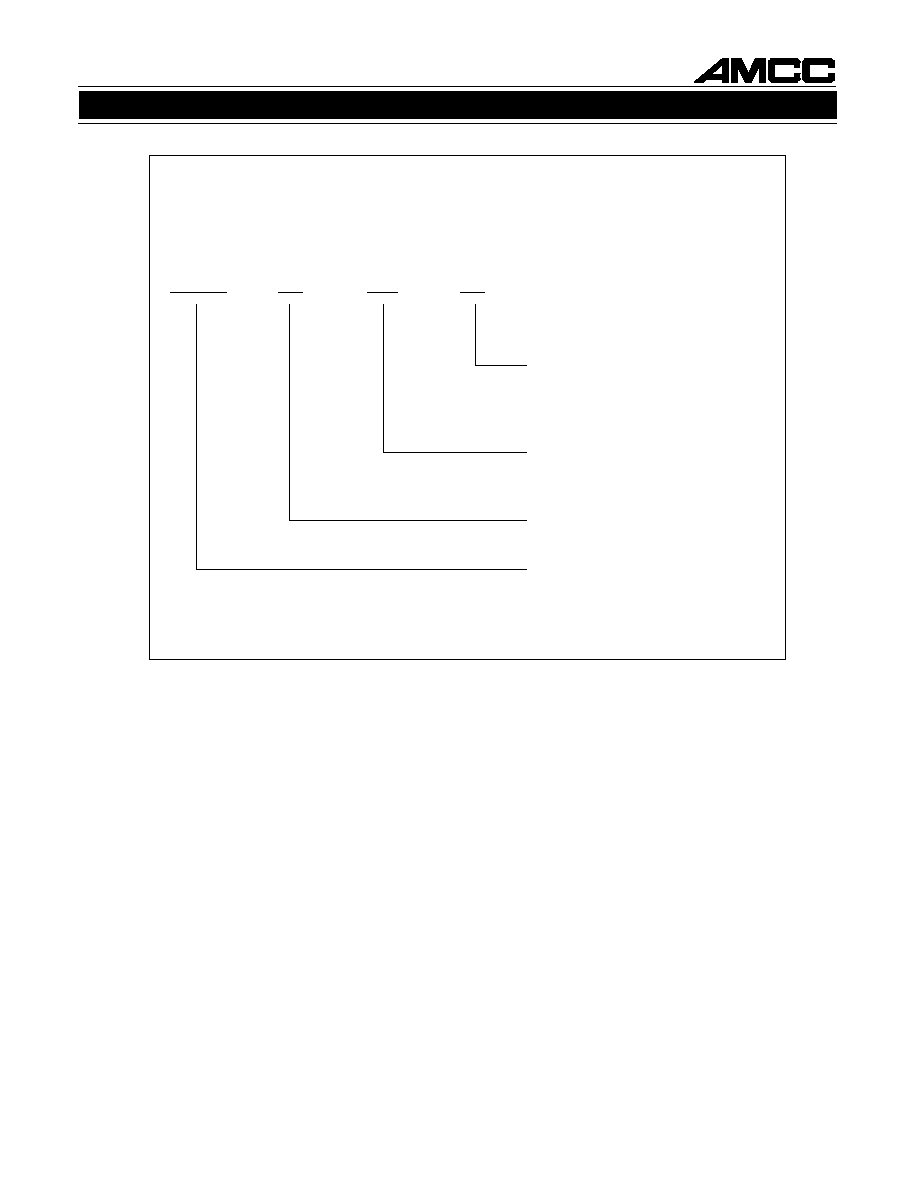
Figure 5. Timing Waveforms
TTLREF, PECLREF
REF
MPW
FBCLK
FOUT0≠3
OUTEN0≠2
t
PE
REF
MPW
HFOUT, X2FOUT
t
SKEW
t
SKEW
t
OFD
t
OFE
Output Valid
Disabled
HFOUT, X2FOUT
FOUT0≠3
PECLP

Applied Micro Circuits Corporation
6195 Lusk Blvd., San Diego, CA 92121 ∑ (619) 450-9333
Page 8
S4405
PACKAGE INFORMATION
Figure 6. S4405 44 PLCC Package and Pinout
1
4
3
2
44
42
41
15
12
13
14
16
17
18
5
6
7
8
9
10
11
25
24
23
22
21
20
19
TTLREF
FBCLK
NC
DGND
PECLREFN
PECLREFP
DGND
D +5V
FOUT2
D +5V
DGND
FOUT1
FOUT0
D +5V
DIVSEL
PHSEL0
PHSEL1
AGND
A+5V
A+5V
FILTER
OUTEN0
HFOUT
X2FOUT
DGND
OUTEN1
PECLP
PECLN
26 27 28
31
34
33
32
30
29
39
38
37
36
35
40
43
FOUT3
LOCK
D +5V
D +5V
DGND
DGND
DGND
DGND
DGND
D +5V
DGND
D +5V
RESET
TESTEN
NC
INPSEL
All dimensions nominal in inches.
Applied Micro Circuits Corporation
6195 Lusk Blvd., San Diego, CA 92121 ∑ (619) 450-9333
Page 9
ORDERING INFORMATION
S4405
AMCC clock driver products are available in several output skew and shipping configurations.
The order number is formed by a combination of:
∑ Device Number
∑ Package Type
∑ Speed Option (if applicable)
∑ Optional Shipping Configuration
S4405
B
≠ 66
/TD
Optional Shipping Configuration
Blank = 28 unit tube
/D = dry pack
/TD = tape, reel and dry pack
Speed Option
≠ 66 = 66 MHz
≠ 80 = 80 MHz
Package Option
B = 44-pin PLCC
Device Number
Example: S4405B≠66/D
44-pin PLCC package, 66 MHz, dry packed in the standard tube.
Ordering Information
AMCC is a registered trademark of Applied Micro Circuits Corporation.
Copyright Æ 1995 Applied Micro Circuits Corporation
Printed in U.S.A./12-08-95
AMCC reserves the right to change specifications for this product in any manner without notice,
and substitute devices manufactured to higher grade levels than ordered.
Applied Micro Circuits Corporation
6195 Lusk Blvd., San Diego, CA 92121 ∑ (619) 450-9333