 | –≠–ª–µ–∫—Ç—Ä–æ–Ω–Ω—ã–π –∫–æ–º–ø–æ–Ω–µ–Ω—Ç: S4406-66 | –°–∫–∞—á–∞—Ç—å:  PDF PDF  ZIP ZIP |
Applied Micro Circuits Corporation
6195 Lusk Blvd., San Diego, CA 92121 ∑ (619) 450-9333
Page 1
S4503
CLOCK SYNTHESIZER
Æ
S4503
BiCMOS CLOCK SYNTHESIZER
FEATURES
∑ Multiplies input reference frequency by
integers 2≠32
∑ Digitally programmable output clock
frequencies from 10 MHz to 300 MHz
∑ Two (2) groups of independent clock outputs
≠ One group consists of differential PECL
outputs
≠ One group is a pair of TTL outputs
∑ Proprietary TTL output drivers with:
≠ Complementary 24 mA peak outputs,
source and sink
≠ Source series termination
≠ Edge rates less than 1.5 ns
∑ Low 250 ps reference typ clock jitter
(PECL outputs), 400 ps max
∑ 1.1 mW or less power dissipation, frequency
and load dependent
∑ 150 MHz to 300 MHz phase-locked loop VCO
frequency range
∑ Advanced BiCMOS process technology
∑ Space saving 28 PLCC package
GENERAL DESCRIPTION
The S4503 is a clock synthesizer which utilizes
phase-locked loop technology to provide two (2) in-
dependently selectable output frequencies in the 10
MHz to 300 MHz range. A reference input may be
provided by either a low cost crystal or a TTL fre-
quency source.
The first of the two (2) output frequency groups con-
sists of a pair of differential PECL (Positive refer-
enced ECL) outputs which will operate up to 300
MHz. The second group (TTL) consist of two outputs
with selectable frequency, up to 80 MHz.
The final frequency for each group is digitally se-
lected via three programmable counters. One
counter is used to set the internal VCO frequency
between 150 MHz to 300 MHz, and the others are
used to divide the VCO frequency from 2 thru 16
(TTL) and 1, 2 or 4 (PECL).
All phase-locked loop elements are provided on chip
with the exception of the passive components
needed for the loop filter function and VCO.
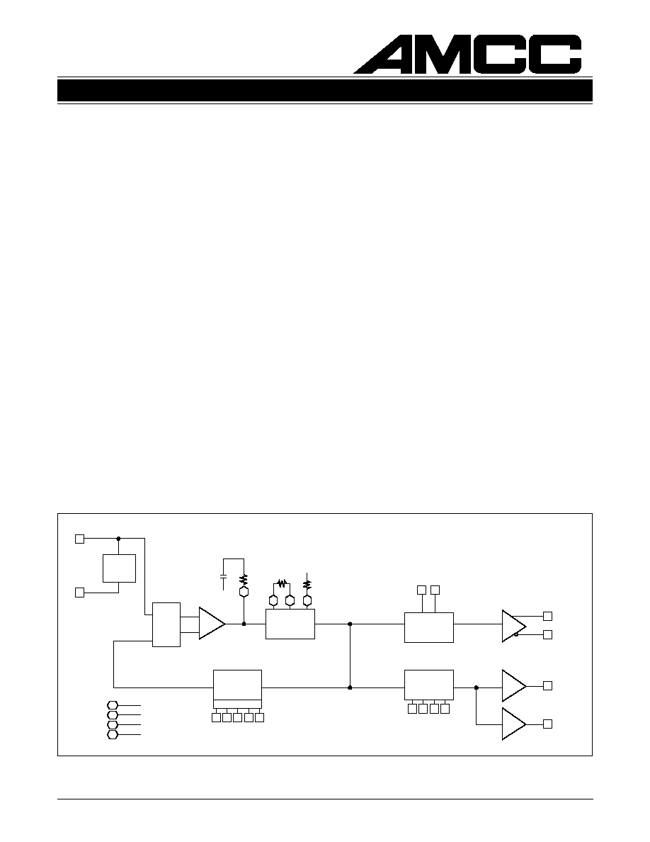
Figure 1. Logic Diagram
VCC
GND
VCCA
GNDA
PHASE
DET
R
F
D
U
M COUNTER
2 to 32
LATCHES
M0
M1
M2
M3
M4
CCOMP
RCOMP
COMP
CHARGE
PUMP
RSPAN
VCCA
RF-CENTER
REXT1 REXT2 KVCO
VCO
(150-300 MHz)
T0
T1
T2
T3
T1 COUNTER
(0, 2 to 16)
P COUNTER
(0, 1, 2, 4)
P0
P1
PECL
OUT
TTL
OUT
TTL
OUT
POUT
POUTN
TOUT1
TOUT1A
GNDA
XTALIN
XTALOUT
XTAL
DRIVER
DEVICE SPECIFICATION

Applied Micro Circuits Corporation
6195 Lusk Blvd., San Diego, CA 92121 ∑ (619) 450-9333
Page 2
S4503
CLOCK SYNTHESIZER
Absolute Maximum Ratings
Storage Temperature ....................... -55
∞
C to +150
∞
C
V
CC
Potential to Ground ..................... -0.5V to +7.0V
Input Voltage ........................................ -0.5V to +V
CC
Static Discharge Voltage ............................... >1750V
Maximum Junction Temperature ................... +130
∞
C
Latch-up Current .......................................... >200 mA
Operating ambient temperature ............ 0
∞
C to +70
∞
C
Capacitance (package)
Input Pins ......................................................... 5.0 pF
TTL Output Pins ............................................... 5.0 pF
PECL Output Pins ............................................ 5.0 pF
SKEW T-T
VCO
XTL
TTL
out
OUTn
SYM-T
SYM-P
J
OUT
Symbol
Description
Conditions
MIN
MAX
Units
F
VCO Frequency
150
300
MHz
F
XTL Frequency, Fundamental
XTLIN to XTLOUT
5
25
MHz
F
TTL Input Frequency
Standard TTL Levels
5
80
MHz
P
PECL Out Frequency
37
300
MHz
T
TTL Out Frequency
See Note 4
9
80
MHz
T
TTL to TTL Output Skew
TTL Leading Edges at +1.5V
250
ps
T
T Symmetry
Measured at 1.5V
±
1.5
ns
T
PECL Out Symmetry
Measured at differential crossing points
±
250
ps
T
PECL Clock Jitter, pk to pk
400
ps
AC Characteristics
V
CC
= +5.0V
±
5%, T
a
= 0
∞
C to +70
∞
C
Notes:
1. Max cycle to cycle jitter.
2. Output symmetry is the deviation from a 50% duty cycle.
3. All AC parameters are tested or guaranteed by characterization.
4. VCO frequency is limited to a maximum of 250 MHz when TTL outputs are used.
Applied Micro Circuits Corporation
6195 Lusk Blvd., San Diego, CA 92121 ∑ (619) 450-9333
Page 3
S4503
CLOCK SYNTHESIZER
Electrical Characteristics
V
CC
= +5.0V
±
5%, T
a
= 0
∞
C to +70
∞
C
1. Maximum test duration one second.
2. All DC parameters are tested or guaranteed by characterization.
The S4503 TTL outputs feature source series termination of approximately 40 Ohms to assist in matching 50≠75
ohm P.C. board environments.
DC Characteristics
The S4503 has been designed specifically for clock distribution. In the development of this product, AMCC has
made several modifications to the historic "high drive, totem pole outputs" producing AMCC's dynamically
adjusting source series terminated outputs. As a result of this, the S4503 will dynamically source and sink a
symmetrical 24 mA of current. In a DC state, it exhibits the following specifications:
Conditions
Min
Max
2.4V
0.6V
V
OL
I
OL
= 4 mA
V
OH
I
OH
= -8 mA
OH
OL
Symbol
Parameter
Conditions
Min
Max
Units
V (PECL)
Output HIGH Voltage, ECL
50 Ohms to V -2V
V -1075
V -650
mV
V (PECL)
Output LOW Voltage, ECL
50 Ohms to V -2V
V -1980
V -1585
mV
V (TTL)
Output HIGH Voltage
F = 80 MHz max,
2.4
V
V (TTL)
Output LOW Voltage, TTL
F = 80 MHz max,
0.6
V
V (TTL)
Input (TTL) HIGH Voltage
All TTL Inputs
2.0
V
V
I (TTL)
Input (TTL) LOW Voltage
All TTL Inputs
-0.5
0.8
V
I (PECL)
Output HIGH Current
50 Ohms to V -2.0
25
mA
I (PECL)
Output LOW Current
50 Ohms to V -2.0
8
mA
I (TTL)
Input HIGH Current
200
uA
I (TTL)
Input LOW Current
50
uA
I
Output HIGH Short Current
Output High, V = V, Typical
-55
mA
I
Output LOW Peak Current
Output Low, V = V
55
mA
I
Supply Current
TTL Outputs to 20 pF @ 50 MHz
210
mA
POWER
Power Dissipation
TTL Outputs to 20 pF @ 50 MHz
1.1
W
OH
OL
IH
IL
OH
OL
IH
IL
OHS
1
OLS
1
CC
CC
OUT
OUT
CC
CC
CC
V
in
= V
CC
V
in
0.8
OUT
OUT
CC
, Typical
C
L
= 10pF
C
L
= 10pF
CC
CC
CC
CC
0
Applied Micro Circuits Corporation
6195 Lusk Blvd., San Diego, CA 92121 ∑ (619) 450-9333
Page 4
S4503
CLOCK SYNTHESIZER
DESCRIPTION OF OPERATION (Refer to
Logic Diagram)
The S4503 synthesizer employs a phase locked loop
(PLL) which includes a "multiplying" counter to produce
a high frequency internal reference oscillator from a
low cost, low frequency crystal. This high frequency
internal reference is the output of a votage controlled
oscillator or VCO. This single VCO frequency is sub
divided down to selectable TTL output frequencies.
One positive (+5V) referenced complementary ECL
(PECL) output (Pout) pair is also provided.
The M counter is a frequency "multiplying" feedback
counter that divides down the VCO frequency, be-
fore applying it to the phase detector. Thus the VCO
frequency is the product of the input reference (crys-
tal) frequency and the M counter modulus. This di-
vide down counter modulus is externally selected to
any integer value from 2 to 32 by a five bit binary
coded value, plus 1, entered into input latches via
the preset input pins M0 through M4. The M0 to M4
inputs have the binary weight of M0=2
0
through
M4=2
4
. The M0-4 inputs are low or 0 if not connected.
NOTE: an entry of all binary zeros will not count down
and is, therefore, invalid. Designs that will load the M
counter inputs from an external register that powers-
up with the outputs in a hi-Z state will need to use
external resistors to ensure the S4503 M counter
inputs are never all zeros.
The output frequency divide down counters "P & T"
each have individual select input pins which may be
actively driven by CMOS/TTL outputs or strapped to
+Vcc (as a 1) or non-connected as appropriate. Non-
connected inputs are biased low or 0. When the bi-
nary coded value of zero is entered into these
counter preselect inputs, their outputs are disabled,
thereby saving AC output power. Note that the input
frequency to the T counter (VCO frequency) is limited
to 250 MHz. P counter will operate up to 300 Mhz.
Output symmetry is very close to 50% duty cycle
with both odd and even division modulus due to an
odd division correction employed at the counter's
output. Refer to the counter preset tables for the
binary coded preselect input values to division
modulus.
The TTL output drivers of the T counter are source
series terminated by internal resistors of ~40 Ohms
to avoid the need for external termination. This se-
ries termination was choosen to match 50 to 75 Ohm
transmission line traces into end of line load capaci-
tance of ~20 pF. Refer also to the AMCC Clock Driver
Application Note #1. The complementary PECL out-
put emitter followers can source 25 mA from +Vcc
and should be externally terminated at the end of the
transmission line into an equivalent 50 Ohm resis-
tance to +Vcc - 2V.
The analog VCO circuitry requires some external
passive loop filter components mounted very close
to the required S4503 package pins. A VCO fre-
quency centering resistor, RFcenter, is connected
between KVCO and +VCCA, the analog +5V. A fre-
quency span resistor, Rspan, is connected between
pins REXT1 and REXT2. A loop filter series resistor-
capacitor pair, RCOMP & CCOMP is connected be-
tween pin Comp and analog ground GNDA. Note
that the analog ground (GNDA) and +5V (+VCCA)
are to be isolated (decoupled) from the noisier digital
and output power leads VCC and GND.
The input to the XTALIN pin will be a series resonant
crystal of fundamental frequency from 5 to 25 Mhz.
The external addition of series or shunt capacitance to
"pull" the frequency is up to the user's discretion. An
external series resistor may be required to limit the drive
current from the XTALOUT pin with low ESR crystals.
When the XTALIN pin is driven by an external TTL
clock source, the XTALOUT pin is not connected and
the peak TTL amplitude should not exceed 3 volts. TTL
output signals should be in the range of 5-80 MHz.
System GND
System VCC
VCCA
GNDA
S4503
21
20

Applied Micro Circuits Corporation
6195 Lusk Blvd., San Diego, CA 92121 ∑ (619) 450-9333
Page 5
S4503
CLOCK SYNTHESIZER
FILTER AND VCO COMPONENT
SELECTION
The S4503 is designed to operate over a wide range
of VCO frequencies. Because of this, it is necessary
to modify the values of Rspan and Rfcenter in order
to get the best performance at a given frequency.
When operating the S4503 with the VCO in the 150≠
225 MHz region, the values for the VCO components
are:
Rspan = 470 Ohms, Rfcenter = 390 Ohms
When operation the S4503 with the VCO in to 225≠
300 Mhz, the values for the VCO components are:
Rspan = 390 Ohms, Rfcenter = 820 Ohms
The loop filter components, Rcomp and Ccomp, do
not change values at different frequencies. The cor-
rect values for these components are:
Rcomp = 2.7K Ohms, Ccomp = 0.1uF
All of the resistor values are 5% and 1/8 watt.
20pF
2M
CRYSTAL
20pF
S4503
26
25
∑ Decoupling capacitors of 0.1 and 0.01 uF are
needed. Three pairs should be placed as close
to the S4503 power and ground pins as pos-
sible. One pair should be used to decouple the
analog VCC and GND, while the others are for the
digital supplies. The Vtt supply will also need to
be decoupled using 0.1 and 0.01 uF capacitors.
These components should be surface mounted
chip capacitors, to reduce the parasitic induc-
tance.
∑ No dynamic signal lines should pass through or
beneath the filter circuitry area, to avoid the
possibility of noise due to crosstalk.
∑ The crystal oscillator will need to have a 2 M
ohm shunt resistor connected between the ter-
minals of the external crystal, and two 20 pF
capacitors connected from each pin of the crys-
tal to VCC (or GND). These components are
necessary to ensure the oscillator will operate at
the correct frequency.
∑ The loop filter and VCO components must be
surface mounted to reduce the parasitic induc-
tance, and the components are connected to the
analog power and ground planes, rather than the
digital planes.
BOARD LAYOUT CONSIDERATIONS
To minimize the impact of board noise on the opera-
tion of the S4503, the following guidelines should be
followed.
∑ The analog VCCA and GNDA need to be iso-
lated from the digital supplies. This can be ac-
complished by creating small analog power and
ground planes next to the S4503 under the filter
and VCO components. These analog planes
can be connected to the digital planes through
wire jumpers, small inductors (5-100 uH), or fer-
rite beads. If the digital supply noise is too large
(>100mV), the inductors or ferrite beads will be
necessary.