 | –≠–ª–µ–∫—Ç—Ä–æ–Ω–Ω—ã–π –∫–æ–º–ø–æ–Ω–µ–Ω—Ç: S4503 | –°–∫–∞—á–∞—Ç—å:  PDF PDF  ZIP ZIP |

6290 Sequence Drive, San Diego, California 92121-4358
800-755-2622 Fax: 619-450-9885
http://www.amcc.com
S5920
32-Bit PCI Bus Target Interface
February 12, 1997 Revised October 1998
F
EATURES
∑
PCI 2.2 Compliant Target/Slave Device
∑
Full 132 Mbytes/sec Transfer Rate
∑
PCI Bus Operation DC to 33 Mhz
∑
Add-On Bus 8 MHz to 40 Mhz
∑
Programmable Prefetch and Wait States
∑
8/16/32 Bit Add-On User Bus
∑
Four Definable Pass-Thru Regions
∑
32 Byte Burstable PCI Bus FIFO
∑
Active/Passive Add-On Bus Operation
∑
Mail Box Registers w/Byte Level Status
∑
Direct Mail Box Data Strobe/Interrupt Pin
∑
Mail Box Read/Write Interrupts
∑
Direct PCI & Add-On Interrupt Pins
∑
S5933 PCI Target Mode Replacement
∑
S5933 Software Compatible
∑
Plug-N-Play Compatible
∑
Two Wire Serial Bus nvRAM Support
∑
Optional External BIOS
∑
160 Pin PQFP
A
PPLICATIONS
∑
ISA to PCI Local Bus Conversions
∑
I/O Communications Ports
∑
High Speed Data Output
∑
General Purpose PCI Interfacing
∑
Data Communications
∑
Memory Interfaces
∑
Data Acquisition
∑
Data Encryption/Decryption
D
ESCRIPTION
The AMCC S5920 was developed to provide the designer with a single multi-function device offering a flexible and
easy means to connect applications to the PCI Local Bus. Designers connecting to the PCI Local Bus through the S5920
eliminate the necessity to understand complex PCI Bus timing requirements and the time consuming task of assuring
PCI specification compliance. The S5920's design incorporates years of design experience and system knowledge
achieved through the popular S5933 PCI Matchmaker device.
The S5920 converts complex PCI bus signals into an easy-to-use 8-, 16- or 32-bit user bus referred to as the Add-On
Local Bus. The S5920 Add-On signal pins, shown in Figure 2, provide the designer with a much simpler bus structure
in which to interface I/O, memory or data acquisition applications and to port existent ISA-based designs over to the
PCI Bus. The bus can be operated either synchronously or asynchronously to the PCI Local Bus with user definable
clock speeds from 8 to 40 MHz.
Since the S5920 is a PCI `Target' or `Slave' device only, its cost is significantly less than PCI Bus Master solutions
making it ideal for low cost applications. The S5920 is compliant with the PCI Local Bus Specification Revision 2.2. It
is capable of 132 Mbytes/sec data transfer rates and supports both burst and single DWORD data transfers. The S5920
logic core is powered from a single 5 volt supply and utilizes advanced AMCC technology to achieve low system power
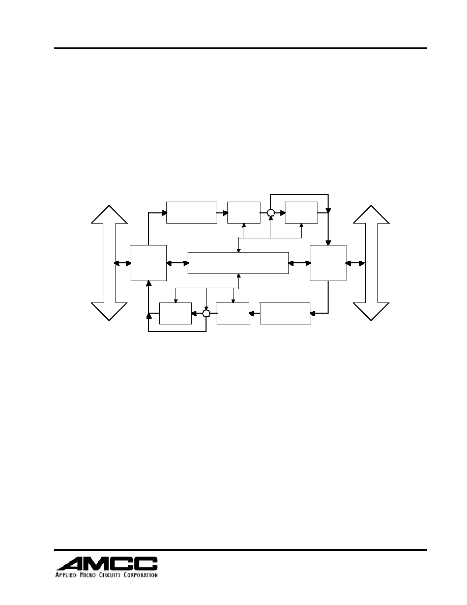
consumption at clock speeds to 33 MHz. The S5920 block diagram is shown in Figure 1.
The S5920's superior feature set offers the designer multiple hardware and software design options for higher perfor-
mance. Up to four Host bus memory or I/O space definable blocks, referred to as Pass-Thru regions, may be imple-
mented providing multiple data channels. Data transfers via a Pass-Thru data channel can be performed through a single
buffered to the application or through burstable FIFOs. Added read prefetch and programmable FIFO wait state features
allow the user to fine tune system performance. The Pass-Thru data channels also supports an `active or passive' mode
bus interface. Passive mode requires the designer to transfer data by externally driving data onto the Add-On Bus.
Active mode minimizes design components by enabling internal logic to drive or acquire the Add-On Bus for reading or
writing data independently. Active mode also supports programmable wait state generation for slower Add-On designs.

6290 Sequence Drive, San Diego, California 92121-4358 800-755-2622
2
S5920
32-Bit PCI Bus Target Interface
Add-On Bus
Timing/Interrupts
S5920 Data
Access Control
Pass-Thru
Control/Access
Serial Bus
Config/BIOS Opt.
PCI
Local
Bus
S5920
Control
Add-On Data Bus
Add-On Bus
Control
Mail Box
Access/Control
BPCLK
ADCLK
SYSRST#
IRQ#
ADDINT#
DQ[31:0]
SELECT#
ADR[6:1]
BE[3:0]#
RD#
WR#
PTATN#
PTBURST#
PTNUM[1:0]
PTBE[3:0]#
PTADR#
PTWR
PTRDY#/WAIT#
DXFER#
PTMODE
DQMODE
MD[7:0]
LOAD#
MDMODE
SDA
SCL
PCLK
INTA#
RST#
AD[31:0]
C/BE[3:0]#
FRAME#
DEVSEL#
IRDY#
TRDY#
IDSEL#
STOP#
LOCK#
PAR
PERR#
SERR#
FLT#
S5920
P
C
I
L
o
c
a
l
B
u
s
User
Application
Serial Bus
Operation/Status
Registers
Mailboxes/Status
Pass-Thru Address
Register
PCI
Pass-
Thru
32-Byte
FIFO
Add-On
Pass-
Thru
2.1 PCI Local Bus
Interface Logic
Mux/Demux
Data Buffers
Serial
Read/Write
Control
PCI Configuration
Registers
Satellite
Receiver/
Modem
Proprietary
Backplane
Graphics/
MPEG/
Grabber
ISDN
FDDI
ATM
ISA
Design
Serial nvRAM
Configuration Space
Expansion BIOS
32-Byte
FIFO
AMCC
Add-On
Local Bus
Interface Logic
Mux/Demux
Active
R/W Logic
Buffers
Serial
Read/Write
Control
The S5920 signal pins are shown in Figure 2.
The PCI Local Bus signals are detailed on the
left side; Add-On Local Bus signal are detailed
on the right side. All additional S5920 device
control signals are shown on the lower right side.
The S5920 provides two 32-bit mailbox registers
for data transfers or user definable status/com-
mand information transfer. Each mailbox may be
examined for an empty or full status, at the byte
level, through a mailbox status register. Mailbox
transfers can be performed either by register
style accesses (RD#/WR#, ADR[6:2], Select#,
etc.) or hardware style accesses (MD[7:0] and
Load#). The dedicated external mailbox data and
strobe signal pins are provided for direct hard-
ware read/writes with additional Add-On to PCI
interrupt capabilities. A direct PCI to Add-On
Bus interrupt pin is also provided adding further
design flexibility.
The S5920 supports a two wire serial nvRAM
bus. This allows the designer to customize the
S5920 configuration by loading setup informa-
tion during system power-up initialization from
a single nvRAM and gain access to other devices
on the serial bus.
Figure 2
Figure 1

6290 Sequence Drive, San Diego, California 92121-4358 800-755-2622
3
S5920
32-Bit PCI Bus Target Interface
S5920
SCL
SDA
4.7K
A0
A1
A2
4.7K
Serial
nvRAM
V
cc
V
cc
Device ID
PCI Status
Class Code
Base Address Register 0
Base Address Register 2
Base Address Register 4
Reserved Space
Expansion ROM Base Address
Reserved Space
Built-In Self Test
Header Type
Subsystem ID
Reserved Space
Max. Latency
Min. Grant
Vendor ID
PCI Command
Revision ID
Base Address Register 1
Base Address Register 3
Base Address Register 5
CacheLine Size
Latency Timer
Subsystem Vendor ID
Interrupt Line
Interrupt Pin
Byte 3
Byte 2
Byte 0
Byte 1
Address
00h
04h
08h
0Ch
10h
14h
18h
1Ch
20h
24h
28h
2Ch
30h
34h
38h
3Ch
The S5920 Register Architecture
All S5920 communications, control and configuration set up is performed through three groups of registers: PCI Configu-
ration Registers, PCI Operation Registers and Add-On Operation Registers. All of these registers are user configurable
through their associated buses with boot loadable registers configured from the external nvRAM. The following provides a
brief overview of each register group.
The S5920 supports boot loading of configuration
data, Expansion BIOS and Power-On Self test code
via the external nonvolatile serial memory device. The
serial nvRAM may be programmed with user-defined
configuration information which is loaded into the
S5920 during power up initialization. Programming
or reading the nvRAM may be done any time from
dedicated S5920 operation registers. The utilization of
the Expansion BIOS feature allows product identifica-
tion banners or other user software code set-up
requirements to be implemented during power up ini-
talization. The serial nvRAM connections are shown
in Figure 3.
Figure 3
PCI Configuration Registers
All PCI compliant devices are required
to provide a group of PCI configuration
registers. These registers are polled by
the host system BIOS during power-up
initialization. They contain specific
device and product information such as
Vendor ID, Device ID, Subsystem Ven-
dor ID, memory requirements, etc.
These registers are located in the S5920
and are either initialized with predefined
default values or user customized defini-
tions contained in the external nvRAM.
Table 1 shows the S5920 PCI Configura-
tion registers.
PCI Operation Registers
The second group of registers, shown in
table 2, are the PCI Operation Registers.
This group of registers is accessible via
the PCI Bus. These are the primary reg-
isters through which the PCI Host con-
figures the S5920 operation and
communicates with the Add-On Bus.
These registers encompass the PCI bus
mailboxes, Pass-Thru/FIFO data chan-
nel and Status/Control registers.
Table 1

6290 Sequence Drive, San Diego, California 92121-4358 800-755-2622
4
S5920
32-Bit PCI Bus Target Interface
PCI Operation Registers
Outgoing Mailbox Register (OMB)
Incoming Mailbox Register (IMB)
Mailbox Empty/Full Status Register (MBEF)
Interrupt Control/Status Register (INTCSR)
Reset Control Register (RCR)
Pass-Thru Configuration Register (PTCR)
Address
Offset
0Ch
1Ch
34h
38h
3Ch
60h
Add-On Bus Operation Registers
Add-On Incoming Mailbox Register (AIMB)
Add-On Outgoing Mailbox Register (AOMB)
Add-On Pass-Thru Address Register (APTA)
Add-On Pass-Thru Data Register (APTD)
Add-On Maibox Empty/Full Status Register (AMBEF)
Add-On Interrupt Control/Status Register (AINT)
Add-On Reset Control Register (ARCR)
Add-On Pass-Thru Configuration Register (APTCR)
Address
Offset
0Ch
1Ch
28h
2Ch
34h
38h
3Ch
60h
8
8
8
8
P
C
I
B
u
s
8
Mailbox
Byte 0
Mailbox
Byte 1
Mailbox
Byte 2
Mailbox
Byte 3
Mailbox Status Register
8
8
8
32
Add-On
Decode
Control
32
PCI
Decode
Control
32
Mailbox
Byte 0
Mailbox
Byte 1
Mailbox
Byte 2
Mailbox
Byte 3
8
/
1
6
/
3
2
A
d
d
-
O
n
B
u
s
32
32
Mailbox Operation
The mailbox registers are divided into two 4 byte sets. Each set is dedicated to one bus for data transfer to the other bus.
Figure 4 shows a block diagram of the mailbox section of the S5920. The provision of mailbox registers provides data or
user defined command/status transfer capability between two busses. An empty/full indication for each mailbox register,
at the byte level, is determined by polling a status register accessible to both the PCI and Add-On busses. Providing mail-
box byte level full indications allows greater flexibility in 8, 16 or 32 bit designs; i.e., transferring a single byte on a 32-
bit Add-On bus without requiring the assembly or disassembly of 32 bit data.
A mailbox byte level interrupt feature for PCI or Add-On busses is provided. Bit locations configured within the S5920
operation registers can select which mailbox byte is to generate an interrupt when the mailbox is written to. Interrupts can
Add-On Bus Operation Registers
The last register group consists of the Add-On Operation Registers shown in table 3. This group of registers is accessible
via the Add-On Bus. These are the primary registers through which the Add-On application configures S5920 operation
and communicates with the PCI Bus. These registers encompass the Add-On bus mailboxes, Pass-Thru/FIFO Registers
and Status/Control Registers.
Table 2
Table 3
Figure 4
6290 Sequence Drive, San Diego, California 92121-4358 800-755-2622
5
S5920
32-Bit PCI Bus Target Interface
P
C
I
B
u
s
Pass-Thru
Register
Endian
Conv.
32-Byte
FIFO
Status/CTRL Register
Add-On
Decode
Control
32
PCI
Decode
Control
32
8
/
1
6
/
3
2
A
d
d
-
O
n
B
u
s
32
Endian
Conv.
32-Byte
FIFO
Pass-Thru
Register
32
has been requested. User logic decodes these signals to determine if it must read or write data to the S5920 to satisfy the
PCI request. Information decoded includes: PCI read/write transaction request, the byte lanes involved, the specific Pass-
Thru region accessed and the request is a burst or single cycle access.
Pass-Thru operation supports single PCI data cycles and PCI data bursts. During PCI burst operations, the S5920 is capa-
ble of transferring data at the full PCI bandwidth. Should slower Add-On logic be implemented, the S5920 will issue a
PCI bus retry until the requested transfer is completed.
To increase data throughput, the Pass-Thru channel incorporates two 32 byte FIFOs. One FIFO is dedicated to PCI read
data while the other is dedicated to PCI write data. Enabling the write FIFO allows the S5920 to accept zero wait state
bursts from the PCI bus regardless of the Add-On bus application design speed.
Enabling the read FIFO allows data to be optionally prefetched from the Add-On Bus. This can greatly improve perfor-
mance of slow Add-On bus designs. PCI read cycles can be performed with zero wait states since data has been
prefetched into the FIFO. Either of the write/read FIFOs can be disabled or enabled to tune system performance.
The Add-On bus can be operated in two different modes: active or passive. The passive mode of operation mimics that of
the S5933 Add-On bus operation. The user design drives S5920 pins to read or write data. In active mode, the Add-On
Bus is driven from an S5920 internal state machine. This reduces component count in cost sensitive designs. Active mode
also incorporates programmable wait states from 0 to 7.
be generated to the PCI or Add-On buses. PCI Bus interrupts may also be generated from direct hardware interfacing due
to a unique S5920 feature. The Add-On mailbox is hardware accessible via a set of dedicated device pins. A single load
pulse latches data into the mailbox generating an interrupt, if enabled.
Pass-Thru Operation
Pass-Thru region accesses can execute PCI bus cycles in real time or through an internal FIFO. Real time operation allows
the PCI bus to directly read or write to Add-On Bus resources. The S5920 allows the designer to declare up to four individ-
ual Pass-Thru regions. Each region may be defined as 8, 16 or 32 bits wide, mapped into memory or I/O system space and
may be up to 512 MB in size. Figure 5 shows a block diagram of the S5920 Pass-Thru architecture.
Host communications to the Pass-Thru data channel utilizes dedicated Add-On Bus pins to signal that a PCI read or write
Figure 5